Note: Descriptions are shown in the official language in which they were submitted.
~29~ 3
INTERFEROMETRIC SENSOR USING
TIME DOMAIN MEASUREMENTS
B3ckaround of the Invention
Field of the Invention
The present invention relates to optical
interferometers, and, more particularly, to
interferometric sensors such as fiber optic gyroscopes.
Description of the Related Art
Fiber optic rotation sensors typically include a loop
of fiber optic material to which light waves are coupled
such that a pair of light waves propagate around the loop
in opposite directions (i.e., the two light waves are
counterpropagating). When the loop is rotated, a relative
phase difference is induced between the counterpropagating
light waves in accordance with the well-known "Sagnac
effect." The amount of phase difference corresponds to
the rotational velocity of the loop. The
counterpropagating light waves, when recombined, interfera
constructively or destructively to produce an optical
output signal that varies in intensity in accordance with
the rotation rate of the loop. Rotation sensing is
commonly accomplished by detection of this optical output
signal.
A number of devices and techniques have been developed
to process the detected optical output signal to provide
an electrical output signal that represents the velocity
and direction of rotation of the loop. Known devices and
techniques monitor the intensity of the optical output
signal to measure the phase difference between the
counterpropagating light waves to determine the rotational
velocity and direction in accordance with the Sagnac
equation:
~R = 8~NA Q (1)
~c
--1--
~g
where:
~R is the sagnac phase difference caused by
rotation oE the optical loop;
A is the area bounded by the optical loop in
which the light waves counterpropagate;
N is the number of times that the light waves
propagate around the loop before being recombined;
Q is the angular velocity of the loop about an
axis that is perpendicular to the plane of the loop;
and
~ and c are the free space values of the
wavelength and velocity, respectively, of the light
waves applied to the optical loop.
The intensity of the optical output signal is a
function of the Sagnac phase difference ~R between the
two counterpropagating light waves as follows:
IT = Il + I2 + 2~IlI2 cos(~R) (2)
where IT is the intensity of the optical output signal,
and Il and I2 are the individual intensities of the two
counterpropagating light waves.
It has been found that simple measurement of the
intensity of the optical output signal will not provide
sufficient information from which the direction and rate
of rotation can be determined. For example, the
sensitivity of the phase difference measurement is
effectively zero for phase differences that are integral
multiples of ~ (i.e., Q~R = N~ for N = ...-2,-1,0,1,2,...)
because the interference intensity is an even, periodic
function of the phase difference (i.e., the interference
intensity varies as a cosine function as set forth in
Equation 2 above. Thus, small phase differences cannot be
directly measured near a zero rotation rate. Typically,
this difficulty in measuring small phase differences is
--2--
overcome by dynamic biasing wherein an ~dditional phase
modulation is introduced into the closed path around which
the light waves are propagating. A time-varying
modulation with a zero mean amplitude is generally used
rather than a static modulation. The dynamic biasing
causes the phase signal to reach values where the
sensitivity is suitably large so that the phase difference
is readily measurable.
A gyroscope with dynamic biasing can be readily used
to measure small rotation rates. When the phase
modulation is a ha~monic signal of a predetermined
frequency, a small phase shift caused by the rotation of
the optical loop causes the intensity of the optical
output signal to include a time-varying component at the
predetermined frequency. This time-varying component can
be demodulated to provide a measure of the Sagnac phase
shift and thus the rotation rate. Although the dynamic
biasing allows phase differences to be measured with high
sensitivity at low rotation rates, the rotation-induced
interference intensity is periodic and thus cannot be used
directly to measure high rotation rates.
In order to provide an extended dynamic range for
measuring rotation rates, two basic approaches have been
used. One approach is to provide a feedback signal from
the demodulated optical output signal to a second device
in the optical loop. The second device provides an
additional, controllable, non-reciprocal phase difference
and the feedback signal is varied so as to null the
demodulated optical output signal. The feedback signal
required to null the demodulated optical output signal is
monitored to measure the Sagnac phase shift and thus the
rotation rate. The performance of this type of closed-
loop gyroscope depends in part upon the stability,
linearity and phase range of the non-reciprocal phase
shifter used for the second device and upon the
--3--
~9~LSi53
characteristics of the electronics that provides the
feedback signal.
An alternative approach to extending the dynamic range
of an optical fiber gyroscope is an open-loop approach
wherein no feedback is provided to null the demodulated
output signal. All the information necessary to
reconstruct the Sagnac phase difference is included in the
interference intensity caused by the combination of the
rotation and the dynamic modulation. Typically, extensive
signal processing is required to extract the phase
difference information from the optical output signal when
the phase difference i5 not limited to values near zero.
When an extended dynamic range is to be attained, the
signal processing can be quite demanding. In many designs
of open-loop optical gyroscopes and other interferometers,
the quality of the electronic signal processing circuitry,
rather than the quality of the optical circuit, determines
the dynamic range and accuracy of the sensing system.
Both analog and digital processing may be used to
process the optical output signal, and, it is preferable
that most of the processing be performed in the digital
domain. However, typical commercially availahle analog-
to-digital convertors needed to convert the analog
electrical representation of the optical output signal to
digital data do not have sufficient dynamic range to
provids quality digital processing. Thus, complex analog
circuitry is typically required as part of the electronics
that processes the optical output signal. Other
electronic circuitry has been use.d that relies less
heavily upon digital processing. However, generally, the
electronic components must be carefully selected and
stabilized in order to achieve the high accuracy that is
required to provide a sensitive interferometer with an
extended dynamic range.
553
Summary of the Invention
The present invention includes an interferometric
sensor for sansing an ambient effect. The sensor
comprises an interferometer having first and second
optical paths. At least one of the optical paths i5
configured for exposure to the ambient effect. The
interferometer includes a coupling device which couples
the optical paths such that first and second light waves
propagating in the optical paths interfere at the coupling
device to form an optical output signal. The output
signal has a waveform defined by phase differences between
the two light waves. A modulator is coupled to at least
the first optical path to modulate the phase of light
propagating through the first optical path. The modula~or
causes a time varying phase difference between the first
and second light waves at the coupling device. The
waveform includes first and second predetermined points
spaced in time. The two points have a time domain
separation which is responsive to the ambient effect. The
int~rferometer further includes a signal processing
circuit and a photodetector. The signal processing
circuit detects the time domain separation between the
first and second points to sense the ambient effect.
In a rotation sensor constructed in accordance with
the present invention, the optical paths are formed by a
loop of optical fiber, and the ambient effect is a
rotationally induced Sagnac effect.
In particular embodiments of the invention, the
predetermined points correspond to points of zero slope of
the waveform. One of the points corresponds to a first
maximum of the waveform, and the other of the points
corresponds to a second maximum of the waveform.
Alternatively, the two points correspond to first and
second minima of the waveform.
~L29~S53
In an exemplary embodiment, the signal processing
circuit comprises a differentiator that dif~erentiates the
waveform to provide a differentiated waveform, and the two
predetermined points correspond to zero-crossings of the
differ~ntiated wavefo~n. The signal processing circuit
further includes a zero-crossing detector that detects the
zero-crossings corresponding to the predetermined points,
and a circuit that measures the time domain separation
between the zero crossings.
In preferred embodiments of the invention, the
waveform includes third and fourth predetermined points,
and the circuit measures the time domain separation
betw~en the third and fourth points. The signal
processing circuit further comprises a comparator that
compares the time domain separation of the first and
second points with the time domain separation of the third
and fourth points to dynamically measure changes in the
phas~ excursion of the modulator.
Preferably, the phase excursion caused by the
modulator is at least 2~ radians so as to produce well-
defined maxima and minima in the waveform of the output
signal. In exemplary embodiments, the phase excursion
ranges from a value between ~ and 2~ radians to a value
between -~ and -2~ radians.
The present invention further includes a method of
sensing an ambient effect that comprises the steps of
propagating first and second light waves in first and
second optical paths, and combining the pair of light
waves after propagation through the optical path to form
an optical output signal. The method further includes the
steps of varying the phase of the light waves to cause the
optical output signal to vary in accordance with a
waveform that includes two predetermined points haviny a
time~domain separation responsive to the ambient effect,
and sensing the two predetermined pcints to measure the
, -6-
S~;3
ambient effect. In an exemplary method of rotation
sensing in accordance with the present invention, the
optical paths ar0 formed by a loop of optical fiber, and
the first and second light waves counterpropagate in the
loop.
Preferably, the two predetermined points comprise
points of zero slope on the waveform, and the sensing step
comprises measuring the time-domain separation between the
points of zero slope. The sensing step includes the steps
of differentiating the waveform to provid~ a second
waveform having zero crossings corresponding to the points
of zero slope, and detecting the zero crossings to measure
the time-domain separation.
In the preferred embodiment, the interferometer is a
Sagnac interferometer having an open loop configuration,
as opposed to a closed loop configuration. As is well
known, in a closed loop interferometer the optical output
signal is fed back to drive the phase modulator, typically
to null the output signal. The magnitude of the driving
signal is indicative of the rotation rate. In contrast,
an open loop gyroscope does not utilize such feedback, and
the rotation information is contained in, and obtained
directly from, the optical output signal. By utilizing an
open loop configuration, the present invention eliminates
complex feedback responsive modulation circuits. When
utilized with a digital detection scheme, the invention is
elegant in its simplicity.
Brief Description of the Drawinas
Figure 1 is a schematic drawing of a Sagnac
interferometer, showing fiber optic components positioned
along a continuous, uninterrupted length of fiber optic
material, and further showing a photodetector that detects
the optical output signal and processing circuitry to
process the electrical signal generated by the
photodetector.
--7--
9~l553
Figure 2 is a schematic drawing of the interferomster
of Figure 1 with the phase modulator removed therefrom.
Figura 3 is a graph of the intensity of the optical
output signal, as measured by the photodetector, as a
function of the rotationally-induced Sagnac phase
di~ference.
Figure 4 is a graph of phase difference as a function
of time, showing the phase modulation of each of the
counterpropagating light waves and the phase diffPrence
between the counterpropagating light waves.
Figure 5 is a schematic drawing illustrating the
effect of the phase modulation upon the intensity of the
optical output signal, as measured by the photodetector,
when the sensing loop is not rotating.
Figure 6 is a schematic drawing showing the effect of
the phase modulation upon the intensity of the optical
output signal, as measured by khe detector, when the
sensing loop is rotating in a first direction.
Figure 7 is a schematic drawing showing the effect of
the phase modulation upon the intensity of the optical
output signal, as measured by the detector, when the
sensing loop is rotating in a second direction, opposite
the first direction.
Figure 8 is a schematic drawing similar to Figure 5
illustrating the effect of a triangular phase modulation
upon the intensity of the optical output signal, as
measured by the photodetector, when the sensing loop is
not rotating, and further illustrating an electrical
waveform produced by differentiating the electrical output
of the photodetector.
Figure g is a schematic drawing similar to Figure 8
illustrating the effect of a triangular phase modulation
upon the intensity of the optical output signal, as
measured by the photodetector, when the sensing loop is
rotating, and further illustrating an electrical waveform
--8--
~2~iiS3
produced by differentiating the electrical output of the
photodetector.
Figure 10 is a schematic drawi.ng of an enlarged
portion of the triangular modulation waveform of Figure 8.
Figure 11 is a schematic drawing of an enlarged
portion of the triangular modulation waveform of Figure 9.
Figure 12 is a block diagram of an exemplary
embodiment of the apparatus of the present invention
showing the rotation sensorl the photodetector, the
electrical differentiating circuit connected to the
electrical output of the photodetector~ the zero-crossing
detector, and the counter/timar circuit.
Figure 13 is a block diagram of an exemplary
embodiment of the counter/timer circuit of Figure 12.
Figure 14 is a schematic drawing similar to Figure 9
illustrating the effect of a sinusoidal phase modulation
upon the intensity of the optical output signal, as
measured by the photodetector, when the sensing loop is
rotating, and further illustrating an electrical waveform
produced by differentiating the electrical output of the
photodetector.
Figure 15 is a schematic drawing of an enlarged
portion of the sinusoidal modulation waveform of Figure
14.
Detailed Description of the Preferred Embodim.ent
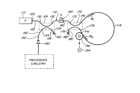
A shown in Figure 1, an open loop rotation sensor
includes a light source 110 that introduces light into a
continuous length of a first optical fiber 112. A
portion of the first optical fiber 112 .is wound into a
sensing loop 114. The first optical fiber 112 is
preferably a single-mode optical fiber having, for
example, an outer cladding diameter of about 80 microns
and an inner core diameter of about 4 microns. The
single-mode fiber 112 is preferably a high birefringence
fiber, although non-birefringent fiber may also be
_g_
9~5LSi53
utilized. The sensing loop 114 comprises a plurality of
turns of the first optical fiber 112 wrapped around a
spool or other support (not shown~. By way of specieic
example, the sensing loop 114 may comprise approximately
looo turns of the ~irst optical ~iber 112 wound on a ~orm
having a diameter of approximatQly 14 centimeters.
Pre~erably, the sensing loop 114 is wound
symmetrically, starting from the center of the length of
fiber in the loop 114, so that ~ymmetrical points in the
loop are in proximlty. Symmetrical winding of the sensing
loop 114 reduces the envlronmental sensitivity of the
rotation sensor 100 because the symmetry causes time-
varying temperature and pressure gradients to have a
similar effect on both counterpropagating wave~ in the
sensing loop 114.
Light from the light source 110 is optically coupled
to one end of the ~irst optical fiber 112 by, for example,
butting a first end 120 o~ the first optical fiber 112
against the light source 110. An input end portion (or
first end portion) 122 of the first optical fiber 112
provides an optical path from the first end 120 to a first
directional coupler 124 that is ~ormed on the first
optical fiber 112. The first directional coupler 124 is
advantageously constructed in accordance with U.S. Patent
Nos. 4,493,528 and 4,536,058. The first directional
coupler 124 has a first port 130, a second port 132, a
third port 134, and a fourth port 136. The first optical
fiber 112 passes through the first directional coupler 124
between the first port 130 and the second port 132, and
continues as an intermediate portion 140 of the first
optical fiber 112. Within the first directional coupler
124, the first optical flber 112 is juxtaposed with a
second optical fiber 150 which may be of the same type as
th~ rir~t ~iber 112, ~h~ ~oond fibG~ 150 ha~ a ~ir~t and
portion 152 and
--10--
553
a second end portion 154. The first end portion 152 of
the second optical fiber extends ~rom the third port 134
of the first directional coupler 124 and is optically
coupled to a photodetector 160. The second end portion
154 extends from the fourth port 136 of the first
directional coupler 124, and is terminated non-
reflectively by a light-absorbing terminator 162. ~he
directional coupler 124 is preferably constructed to
couple approximately 50 percent of the light in one of the
optical fibers to the other optical fiber. Accordingly,
approximately 50 percent of the light propagating in the
input end portion 120 of the first optical fiber 112 is
coupled to the end portion 154 of the second optical fiber
150. The other 50 percent of the light exits the second
port 13Z of the first directional coupler 124 and
propagates in the intermediate portion 140.
The intermediate portion 140 of the first optical
fiber 112 provides an optical propagation path from the
first directional coupler 124 to a second directional
coupler 170 that may be constructed in a similar manner to
the first directional coupler 124. The second directional
coupler 170 has a first port 172, a second port 174, a
third port 176, and a fourth port 178. The intermediate
portion 140 of the first optical fiber 112 enters the
second directional coupler 170 at the first port 172.
After passing through the second directional coupler 170
between the first port 172 and the second port 174, the
first optical fiber 112 forms the sensing loop 114, as
discussed abo~e. The first optical fiber 112 then passes
back through the second directional coupler 170 from the
fourth port 178 and the third port 176. A second end
portion 180 of the first optical fiber 112 extends from
the third port 176 and is terminated by a terminator 182
that comprises a light-absorbing material. The second
directional coupler 170 is constructed to have
--11--
5S3
substantially 50 percent coupling efficiency. When light
is input to the second directional coupler 170 via the
first port 172, the light will be split so that the light
output from the second directional coupler 170 will be
divided substantially equally between the two output ports
174 and 178. The light output from the second directional
coupler 170 forms a first light wave, represented by an
arrow W1, that propagates around the sensing loop 114 in a
clockwise direction, as viewed in Figure 1, and a second
light wave, represented by an arrow W2, that propagates
around the sensing loop 114 in a counterclockwise
direction. Thus, the second directional coupler 170 forms
a pair of counterpropagating light waves that traverse the
sensing loop 114. Since the coupling efficiency of the
second directional coupler 170 is 50 percent, the
intensities of the two light waves Wl and W2 are
substantiall~ equal.
After traversing the entire length of the first
optical fiber 112 that forms the sensing loop 114, the
first light wave Wl, enters the second directional coupler
170 via the fourth port 178, and the second light wave W2
enters the second directional coupler 170 via the second
port 174, such that the waves Wl and W2 are recombined.
Approximately 50 percent of the recombined light axits the
first port 172 for propagation to the intermediate portion
140 of the first optical ~iber 112. The remaining 50
percent of the recombined light exits via ~he third port
176 to be absorbed by the light-absorbing terminator 182.
The recombined light waves propagate via the
intermediate portion 140 of the first optical fiber 112 to
the second port 132 of the firsk directional coupler 124.
Approximately 50 percent of the recombined light waves
that enter the second port 132 are coupled to the first
end portion 152 of the second optical fiber 150 via the
third port 134 and propagate to the photodetector 160.
-12-
The pho-todetector 160 outputs an electrical signal that is
proportional to the intensity of the optical output
signal, and the electrical signal is proaessed by a
processing circuit to produce a signal indicative o~ the
rotation rate of the loop.
A polarizer 190 i6 ~dvantageously formed on the
intermediate portion 140 of the first optical ~iber 112
between the first directional coupler 124 and the second
directional coupler 170. The polarizer 190 may be
constructed in accordance with U.S. Patent No. 4,3~6,822~
The polarizer 190 is positioned on the intermediate
portion 140 of the first optical ~iber 112 so that light
of one polarization mode is permitted to pass through the
intermediate portion 140 while the passage of light of an
orthogonal polarization mode is prevented.
As set forth in U.S. Patent 4,410,275, the purpose of
the polarizer 190 is to ensure reciprocal operation of the
rotation sensor of Figure 1. Spurious non-reciprocal
phase differences may occur in the sensor because the
light travelling in each of the two polarization modes of
a single mode fiber, such as the first optical ~iber 112,
travels at a different propagation velocity. Such a non-
reciprocal phase dif~erence is indistinguishable from a
rotationally induced Sagnac phase difference, and is
dependent on environmenta} factors, such as temperature
and pressure. When the polarizer 190 is included, light
passing through the polarizer 190 and into the sensing
loop 114 via the second directional coupler 170 propaga~es
in only a selected one of the two polarization modes.
Furthermore, when the two aounterpropagating light waves
Wl and W2 are recombined to form the recombined optical
signal, any light in the recombined optical signal that
does not have the same polarization as the light applied
-13-
to the sensing loop 114 is prevented ~rom reaching the
first directional coupler 124 and thus does not form part
of the optical output signal that is detected by the
photodetector 160. Accordingly, by pas~ing the input
light ~i.e., the light input to the sensing loop 114) and
the output light (i.e., the light output from the sensing
loop 114) through the same polarizer l90, only a single
optical path is utili~ed for propagating the light waves.
Thus, non-reciprocity caused by the different propagation
velocities of the two polarization modes is eliminated.
The single mode optical ~iber 112 ls preferably a highly
birefringent optical fiber having two well-defined
polarization modes, and the polarizar is adjusted to
select light propagating in one of the two polarization
modes. If non-birefringent fiber is used; it may be
preferable to include a pair of polarization controllers
(not shown) to adjust the polarization of the input
optical signal and the polarization of the light
propagating in the sensing loop so that the polarization
is aligned with the polarization axis of the polarizer
190, thereby reducing optical power loss in the polarizer
190 .
As set forth in U.S. Patent No. 4,529,312, reciprocity
may also be achieved through the use of unpolarized light.
It has been found that unpolarized light causes the non-
reciprocal pha~e errors to cancel.
As further illustrated in Figure 1, a phase modulator
192 is formed on the optical ~iber 112 proximate to the
fourth port 178 of the second directional coupler 170
between the fourth port 178 and the sensing portion 114.
The phase modulator 192 is electrically connected to and
driven by an electrical signal generator 194. The phase
modulator 192 may compri~e a PZT cylinder, around which a
portion of th~ ~ir~t opti~al ~iber 112 is wrappsd. The
-14-
. . ~,
, ~b - `
5~3
first optical fiber 112 is bonded to the Pzrr cylinder so
that when the PZT cylinder expands radially in response to
an electrical modulating signal from the signal generator
194, the portion of the first optical fiber bonded to the
PZT cylinder stretches. Other modulators, such as
electro-optic modulators, can also be used.
In order to understand the function of the phase
modulator 192, the operation of the rotation ~ensor 100
will first be described as if the phase modulator lg2 were
not present. For the purposes of this discussion, the
rotation sensor 100 is illustrated in Figure 2 without the
phase modulator 192. As set forth above, light from the
source 110 traverses the sensing loop 114 and is combined
to form an optical output signal that is detected by the
photodetector 160.
The intensity of the optical output signal received by
the photodetector 160 will vary in accordance with the
amount and type (i.e., constructive or destructive)
interference between the two counterpropagating light
waves W1 and W2 when they are recombined at the second
directional coupler 170. Assuming the sensing loop 114 is
at rest (i.e., is not rotating), the two waves Wl and W2
travel the same optical path around the sensing loop 114.
Thus, when the two waves W1 and W2 are recombined at the
second directional coupler 170, they will interfere
constructively, with no phase difference therebetween, and
the intensity of the optical output signal detected by the
photodetector 160 will be at a maximum. However, when the
sensing loop 11~ is rotated, the counterpropagating light
waves Wl and W2 will be shifted in phase in accordance
with the Sagnac effect, so that when they are superimposed
at the second directional coupler 170, they de~tructively
interfere, thereby causing a reduction in the intensity of
the optical output signal and thus reducing the magnitude
of the electrical output signal generated by the
-15-
ILS53
photodetector 160. The Sagnac phase difference between
the light waves Wl and W2 is defined by the following
relationship:
Q~R = _~_ Q ~1)
where:
Q~R is the Sagnac phase difference caused by
rotation of the optical loop;
A is the area bounded by the optical loop in
which the light waves counterpropagate;
N is the number of times that the light waves
propagate around the loop before being recombined;
Q is the angular velocity of the loop about an
axis that is perpendicular to the plane of the loop;
and
~ and c are the free space values of the
wavelength and velocity, respectively, of the light
waves applied to the optical loop.
The intensity of the optical output signal is a
function of the Sagnac phase difference Q~R between the
two counterpropagating light waves as follows:
IT = Il ~ I2 ~ 2~III2 cs(Q~R) (2)
where IT is the intensity of the optical output signal,
and I1 and I2 are the individual intensities of the two
counterpropagating light waves.
From Equations 1 and 2, it may be seen that the
intensity of the optical output signal is a function of
the rotation rate Q. Thus, an indication of the rotation
rate Q may be obtained by measuring the intensity of the
optical output signal by using the photodetector 160.
Figure 3 shows a curve 200 that illustrates the
relationship between the intensity IT f the optical
output signal and the Sagnac phase difference Q~R between
-16-
~ ~:9~SS3
the two counterpropagating light waves Wl and W2. The
curve 200 has the shape of a cosine curve in accordance
with Equation 2, and the intensity of the optical output
signal is at a maximum when the Sagnac phase differenca
~R is zero or an even multiple of ~ (i.e., ...-4~, -2~,
0, 2~, 4~ ...) and at a minimum when the Sagnac phase
difference ~R is a odd multiple of ~ (i.e., .O.-3~
~, 3~, 5~ ...). When the phase difference between the
counterpropagating waves is caused entirely by rotation of
the sensing loop 114, the curve 200 will vary
symmetrically about a vertical axis 202.
Referring to Figure 3, it can be seen that, because
the curve 200 is a cosine function, the intensity of the
optical output signal detected by the photodetector 160 is
highly nonlinear for small Sagnac phase differences ~R
between the two counterpropagating light waves W1 and W2.
Furthermore, the optical output signal intensity is
relatively insensitive to changes in phase difference for
small changes in the value of ~R- Such nonlinearity and
insensitivity makes it very difficult to transform the
intensity IT f the optical output signal, as measured by
the photodetector 160, into a signal that is indicative of
the rate of rotation of the sensing loop 114 in accordance
with Equations 1 and 2. For example, assuming that the
horizontal axis of the Figure 3 to the right of the
vertical axis 202 represents Sagnac phase differences ~R
caused by clockwise rotation of the sensing loop 114 and
that the horizontal axis to the left of the vertical axis
202 represents Sagnac phase differences ~R caused by
counterclockwise rotation of the sensing loop 114, it can
be seen that the direction of rotation cannot be
determined by simply measuring the intensity of the
optical output signal since the intensity is symmetrical
about the vertical axis 202 and is the same for equal
rotation rates in either direction.
-17-
5~i~
A number of devlces and tea~miques hav~ been used to
measure the rotation rate by modulating the phases of the
two counterpropagating light waves Wl and W2 such that the
intensity of the optical output signal detected by the
photodetector 160 includes suffiaient information so that
small rotation rates can be measured and so that rotation
in the clockwise direction can be distinguished from
rotation in the counterc:lockwise direction. For example,
UOS. Patent Nos. 4,410,275; 4,4S6,377; 4,529,312;
4,634,282; 4,637,722: 4,6B7,330; 4,728,192: and 4,707,136,
disclose devices and techniques for modulating the phase
of the counterpropagating light waves in a sensing loop
and for determining the rotation rate from the inkensity
of the optical output signal.
Referring to Figure 4, the phase modulator 192
modulates the phase o~ each of the counterpropagating
light waves Wl and W2 at the f~requency of the signal
generator 194. As set forth above, the phase modulator
192 is preferably located proximate to the second
directional coupler 170, near one end of the sensing loop
114. Thus, the modulation of the clockwise propagating
light wave Wl is not necessarily in phase with the
modulation of the counterclockwise propagating light wave
W2. The modulation of the light wave Wl is typically 180
--18--
5~
degrees out of phase with the modulation of the light wave
W2. This is illustrated in Figure 4, wherein the
modulation of the phase of the light wave W1 is
represented by a sinusoidal curve 210 that is 180 degrees
out of phase with a sinusoidal curve 212 that represents
the modulation of the phasP of the light wave W2. Use of
a modulation frequency that provides such 180-degrPe phase
difference between the modulation of the light wave Wl
relative to that of the light wave W2 is particularly
advantageous because it eliminates the effects of
modulator induced amplitude modulation in the optical
output signal measured by the photodetector 160. The
preferred modulation frequency fm that provides such
180-degree phase difference between the modulations of the
two l~ght waves may be calculated in accordance with the
following equation:
f = c (3)
2neqL
where:
L is the differential fiber length between the
second directional coupler 170 and the phase modulator
192 for the counterpropagating light waves Wl and W2,
i.e., the distance, measured along the fiber, between
the phase modulator 192 and a symmetrical point on the
opposite end of the sensing loop 114;
neq is the equivalent refractive index for the
optical Piber 112; and
c is the free space veloci.ty of the light applied
to the sensing loop 114.
At the selected modulation frequency fm, which is
often called the "proper frequency", the phase difference
~ between the two counterpropagating light waves Wl and
W2 caused by the phase modulation of the two light waves
is illustrated by a sinusoidal curve 214 in Figure 4. The
--lg--
S~ii3
curve 214 is obtained by subtracting the curve 212 from
the curve 210 to obtain the phase difference between the
light wave Wl and the light wave W2. The modulation of
the phase difference between the light wave Wl and the
light wave W2 also modulates the intensity I~ of the
optical output signal in accordance with the curve 200 of
Figure 3. Such phase modulation ~M is indistinguishable
from rotationally-induced Sagnac phase difference ~R.
The foregoing may be more fully understood by
lo referring to Figures 5 and 6 which graphically illustrate
the combined effect of the phase modulation Q~, defined
by the curve 214 of Figure 4, and the rotationally-induced
Sagnac phase difference ~R, upon the intensity IT f the
optical output signal. It sho~ld be understood that the
intensity IT is a function of the total phase difference
between the light waves W1 and W2, and that the total
phase difference is comprised of both the rotationally-
induced Sagnac phase difference ~R and the time-varying
modulation-induced phase difference ~M. The total phase
difference ~T between the two light waves Wl and W2 may
be expressed as follows:
Q~T = ~R ~ ~M (4)
As indicated above, the effects of the modulation-induced
phase difference Q~M, as well as the rotationally-induced
phase difference ~R, will be considered in reference to
Figures 5 and 6. Accordingly, the horizontal axis for the
graph of the curve 200 in Figures 5 and 6 has been
labelled as ~T to indicate that the total phase
difference is being considered, rather than only the
rotationally-induced phase difference ~R, as in Figure 3.
Referring now to Figure 5, the effect of the phase
modulation ~M (represented by the curve 214) upon the
intensity IT will be first discussed. The curve 200
-20-
~l~9~5;3
represents the relationship between (1) the intensity of
the optical output signal resulting from interference of
the two waves W1 and W2 at the coupler 170, and (2) to the
phase difference Q~T between the two light waves at the
coupler 170. When the modulation-induced phase difference
~M between the two light waves is zero, as illustrated at
a location 220 on the curve 200 in Figure 5, the resultant
intensity I~ of the combined light waves is a maximum~ as
illustrated at the location 222 on the curve 200. When
the relative phase angle between the two light wave~ Wl
and W2 is non-zero, the combined optical signal will have
a lower intensity, depending upon the magnitude of the
phase difference ~M. The intensity continues to decrease
with increasing A~N until the relative phase difference
~M is either plus or minus 180 degreesl as illustrated at
a location 224 and at a location 226, respectively, in
Figure 5. At a phase difference of plus or minus 180
degrees (i.e., +~ or -~), the two counterpropagating light
waves completely destructively interfere, and the
resultant intensity is zero, as illustrated at the
location 224 and the location 226. Since the curve 200 is
a periodic function of the total phase difference ~T, if
the total phase difference ~T is increased beyond +~ or
-~, the intensity will increase, as further illustrated in
Figure 5.
In Figure 5, it is assumed that the sensing loop 114
is at rest, and thus, the optical output signal is not
affected by the Sagnac effect. Specifically, it may be
seen that the modulation-induced phase diference curve
214 causes the intensity IT f the optical output signal
to vary in time, as illustrated by an intensity curve 230
in Figure 5. The intensity curve 230 is obtained by
translating the points on the curve 214 (representing the
instantaneous modulation phase difference A~M between the
two light waves Wl and W2) onto the curve 200
-21~
SS3
(representing the resultant optical intensity for a phase
difference of that magnitude). When all the points on the
curve 214 are translated onto the curve 200, and the
corresponding intensities are plotted, the curve 230
results. At zero rokation, the translation of the curve
214 through the curve 200 is symmetrical about the
vertical axis 202 of the curve 200. Thus, the optical
intensity repr~sented by the curve 230, and measured by
the photodetector 160, varies periodically at a frequency
equal to the second harmonic of the modulating frequency
fm-
When the sensing loop 114 is rotated, the
counterpropagating light waves w1 and w2 are shifted in
phase in accordance with the Sagnac effect, as discussed
above. The Sagnac phase shift provides a constant phase
difference ~R for a constant rotational velocity. The
Sagnac phase shift adds to the phase difference Q~ caused
by the phase modulator 192 so that the entire curve 214 is
translated in phase from the position shown in Figure 5 by
an amount equal to Q~R, as illustrated in Figure 6. The
addition of the rotationally-induced phase difference to
the modulator-induced phase difference causes the
intensity IT f the optical output signal to vary
nonsymmetrically along the curve 200 between a point 240
and a point 242, and thus causes the optical output signal
to have a time-varying intensity as illustrated by a curve
250 in Figure 6.
The curve 250 can be obtained by translating points on
the curve 214 onto the curve 200, as discussed above in
connection with Figure 5. For example, the combined phase
difference ~TI illustrated at a location 260 on the curve
214 translates through a location 262 on the curve 200 to
a location 264 on the curve 250. It should be understood
that the location 264 corresponds in time to the location
260 and corresponds in amplitude to the location 262.
-22-
Similarly, a location 266 on the curve 214 translates
through the location 242 on the curve 200 to a location
268 on the curve 250; a location 270 on the curve 214
translates through the location 262 on the curve 200 to a
location 272 on the curve 250; a location 274 on the curve
214 translates through a location 276 on the curve 200 to
a location 278 on the curve 250; a location 280 on the
curve 214 translates through the location 240 on the
curves 250 to a location 282 on the curve 250; a location
284 on the curve 214 translates through the location 276
on the curve 200 to a location 286 on the curve 250; a
location 288 on the curve 214 translates through the
location 262 on the curve 200 to a losation 290 on the
curve 250; and a location 292 on the curve 214 translates
through the location 242 on the curve 200 to a location
294 on the curve 250. It can be seen that after the curve
214 completes one cycle, for example, from the location
260 to the location 288, and begins repeating, the
corresponding locations on the curve 250 also repeat.
Figure 7 illustrates a curve 300 for the optical
output signal when the phase difference ~R results from
rotation in the opposite direction to the rotation in
Figure 6 and thus causes the curve 214 to be shifted in
the opposite direction along the ~T axis. It can be seen
that for substantially the same magnitude of Sagnac phase
shift ~R, the curve 300, representing the intensity of
the optical output signal, is substantially similar to the
curve 250 in Figure 6; however, the curve 300 is shifted
in phase with respect to the curve 250.
The optical output signal has a first harmonic
component as illustrated by sinusoidal curve 310 (shown in
phantom) in Figure 7. The amplitude of this firs~
harmonic component is indicative of the rotationally-
induced Sagnac phase shift. Thus, by detecting this first
harmonic, an indication of the rotation rate of the
23-
3gl 5~i3
sensing loop 114 may be obtained. An example of a
previous rotation sensor that utilizes this technique is
disclosed in u.S. Patent No. 4,410,275. Such rotation
sensors typically used a lock-in amplifier to
synchronously detect the component of the electrical
representation of the optical output signal to provide an
amplified output signal having a value proportional to the
RMS value of the first harmonic component of the optical
output signal. The amplified output signal is used in
such rotation sensors to indicate the rotation rate of the
sensing loop.
The present invention provides an apparatus and method
for determining the direction and rate of rotation of the
sensing loop 114 that does not require the use of a lock-
in amplifier or other such device. The present invention
is particularly ad~antageous in that it lends itself to
digital processing of the optical output signal.
Figure 8 illustrates a set of four curves. Three of
the curves, 400, 410 and 420, are similar to the three
curves 200, 214, and 300 discussed above in connection
with Figure 7. The curve 400 illustrates the output
intensity IT as a function of the total differential phase
shift ~T between the two counterpropagating light waves
Wl and W2. As before, the curve 400 is cosinusoidal such
that the maximum output intensity IT correspon~s to zero
phase shift and to even multiples of ~ phase shift, and
the minimum output intensity corresponds to odd multiples
of ~ phase shift. The curve 410 represents the time-
varying differential modulation ~Mtt) of the phase caused
by the operation of the phase modulator 192 (Figure 1).
In Figure 8, the curve 410 is illustrated as a triangular
waveform; however, as will be shown below, other waveforms
for the phase modulation (e.g., sinusoidal) can be
alternatively used. In preferred embodiments, the
modulation is symmetrical such that the increasing portion
-2~-
~9~ 3
of the modulation on one side of a maximum (or a minimum)
is mirrored by a corresponding decreasing portion on the
other side of a maximum ~or a minimum) in each half cycle,
and such that the slopes of the increasing and decreasing
portions are finite (i.e., have a well-defined, non-
vertical slope). In Figure 8, it is assumed that the
sensing loop 114 is not rotating so that the time varying
total phase difference ~T(t) between the two light waves
is the same as the differential phase modulation Q~M~t).
The time-varying phase difference ~T(t) translates
through the curve 400 to a curve 420 that represents the
intensity IT(t) of the optical output signal as a function
of time. In Figure 8, the amplitude of the phase
modulation is selected so that the total phase difference
~T has an absolute magnitude that is greater than ~ and
less than 2~. For example, in Figure 8, th~ total phase
difference ~T varies from a magnitude that is between -2~
and -~ to a magnitude that is between +~ and +2~. This
selection of the amplitude of the phase modulation assures
that the phase modulation curve 410 will have an excursion
that passes the minima on the curve 400 at -~ and at +~.
The curve 420 has a number of distinct maxima and
minima that correspond in time to the maxima and minima of
the curve 410, as translated through the curve 400, and a
number of distinct maxima and minima that ¢orrespond to
the maxima and minima of the curve 400. Each of the
maxima and minima on the curve 410 and each of the
locations on the curve 410 that corresponds to a maxima or
a minima of the curve 400 has been labelled with a letter
A, B, C, D . . . ,O, P. The corresponding locations on
the curve 420 have been labelled with the same letter so
that the correspondence can be clearly understood. For
example, at a time tA, the differential phase modulation
~M has a magnitude that corresponds to a differential
phase shift of +~ and thus causes the optical output
-25-
~ ~9~.~;i53
signal to have an intensity substantially equal to zero,
as illustrated by the zero magnitude of the curve 420 at
the time tA (i.e., the location A on the curve 420).
Similarly, at a time tB, the differential phase modulation
~M has a maximum positive magnitude. This magnitude
translates through the curve 400 to a location s on the
curve 420 at the time tB. It can be seen that the
locations A, C, E, G, I, K, M, and O correspond to the
translation of the like-identified locations on the curve
410 through the minima of the curve 400 at phase
differences of -~ and +~; and the locations D, H~ L, and P
on the curve 420 correspond to the translation of the
like-identified locations on the curve 410 through the
maximum of the curve 400 at a phase difference of zero.
The peaks of the curve 420 at the locations B, F, J, and N
correspond to the translation of the like-identified peaks
of the curve 410 through the curve 400. One can see that
the peaks of the curve 420 at the locations B, F, J, and N
will be always spaced apart in time by intervals that are
equal to one-half the period of the selected modulation.
For example, in Figure 8, the period of the phase
modulation is shown as T, and one-half the period of the
modulation is shown as T/2. So long as the frequency of
the phase modulation is held constant, the spacing between
the peaks B, F, J, and N will be constant. On the other
hand, as will be described below in connection with Figure
9, the times at which the maxima and minima of the curve
420 at the locations A, C, D, E, G, H, I, K, L, M, O, and
P occur depends upon whether or not the modulation curve
410 is offset by a rotationally-induced phase difference
Q~R caused by the Sagnac effect.
As set forth above, the amplitude ~Mmax of the curve
410 is selected to be at least ~ so that the phase
excursion of the modulation passes through the minima and
maxima of the curve 400. Preferably, the amplitude Q~Mmax
-26-
~9~S~ii3
is selected to be greater than ~ so that the locations of
zero slope on the curve 420 caused by the minima and
maxima of the curve 400 (e.g., the locations A, C, D, E,
G, H, I, K, L, M, O~ are distinguishable from the
locations of zero slope caused by the peaks of the curve
410 (e.g., the locations B, F, J, N).
Figure 9 illustrates the curve 400 thak corresponds to
the curve 400 in Figure 8, and also illustrates a curve
410' that generally corresponds to the curve 410 in Figure
8. However, in Figure 9, a rotationally-induced phase
difference A~R has been added to the modulated phase
difference curve 410 of Figure 8 so that the modulated
phase difference curve 410' is offset from the zero phase
difference axis in the positive direction (i.e., towards
+~). As in Figure 8, the locations on the curve 410' in
Figure 9 are translated through the curve 400 to produce a
curve 430 that represents the optical output intensity
IT(t) as a function of time. For example, the relative
peaks at the locations B', F', J' I and N' on the curve 430
correspond to the maximum and minimum excursion of the
rurve 410' with respect to the curve 400. The magnitudes
of the peaks at the locations B', F', J', and N' oE the
optical output intensity IT(t) curve 430 in Figure g have
changed with respect to the correspondins locations B, F,
J, and N on the curve 420 in Figure 8 since the maxima and
minima of the curve 410' have shifted with respect to the
differential phase shift axis ~T of the curve 400.
However, the times at which the peaks at the locations B',
F', J', and N' are fixed since they directly correspond to
the times at which the like-identified maxima and minima
of the curve 410 occur. In contrast, the magnitudes oE
the maxima and minima A and A', C and C', D and D', E and
E', G and G', H and H', I and I', K and K'l ~ and L', M
and M', 0 and O', and P and P' are fixed, but the times at
which they occur vary in accordance with the amount of
-27-
Sagnac phase shift ~R that has been added to the phase
modulation ~M. For example, when Figure 9 is compared
with Figure 8, it can be seen that in Figure 9 the two
locations H' and L' on the curve 410' that translate
through the maximum of the curve 400 at 0 have shifted in
time with respect to the locations H and L in Figure 8. In
particular, the locations H' and L' in Figure 9 are æpaced
further apart in time by a time interval ~tl' that is
greater than a corresponding time interval ~tl between the
locations H and L in Figure 8. Similarly, the locations
I' and K' in Figure 9 are spaced apart by a time interval
~t2' that is greater than a corresponding time interval
~t2 between the locations I and K in Figure 8.
The change in the time interval between the locations
H and L and the locations H' and L' and the change in the
time interval between the locations I and K and the
locations I' and K' are directly related to the offset in
the curve 410' relative to the curve 410 in Figure 8
caused by the rotationally-induced Sagnac phase difference
~R. This can be more fully understood by referring to
Figure 10 wherein the portion of the curve 410 in Figure 8
between the locations H and L is expanded for clarity, and
to Figure 11 wherein the portion of the curve 410' between
the locations H' and Lr is expanded for clarity.
Referring first to Figure 10, which represents the
curve 410 when there is no additional phase shift ~R
caused by rotation, it can be seen that the magnitudes of
the time intervals ~tl and Qt2 can be determined by
geometric calculations based upon the maximum amplitude of
the phase modulation ~M(t), shown as ~Mmax. As was
illustrated in Figure 8, and as shown again in Figure 10,
the magnitude of the time interval between the location H
and the location L is ~tl and the time interval between
the location I and the location K is At2. In Figure 10,
the locations H and L represent a phase difference of
-28-
zero and correspond to the maxima on the optical output
intensity curve 420 in Figure 8. The locations I and K
represent a phase difference of ~ and correspond to the
minima on the optical output intensity curve 420 in Figure
8. Thus, the locations H and L are always separated from
the locations I and X by a phase difference of ~ radians.
This is further illustrated in Figure 11 wherein the
locations I' and K' are shown as being separated from the
locations H' and L' by phase angle difference of ~
radians. However, in Figure 11, the time interval ~tl'
between the location H' and the location L' is larger than
the time interval ~t1 between the location H and the
location L in Figure 10. Similarly, the time interval
~t2' between the location I~ and the location K' in Figure
11 is greater than the time interval Qt2 between the
location I and the location K in Figure 10. The change in
the time difference is directly related to the offset in
the phase difference caused by the rotationally induced
phase differenCe ~R-
The relationship between the rotation-induced phase
difference ~R and the points H', L', I', and K' in Figure
11 may be analyzed using geometry. A first triangle is
formed by points X, Y, and Z of the curve 410. The points
X and Y are the points of the curve 410 which are
displaced from zero phase difference by the ~R effect. A
second triangle is formed by points H', L', and Z.
Finally, a third triangle is formed by points I', K', and
Z. The first triangle has a base of T/2 and has a height
of Q~Mmax, which is one-half of the peak-to-peak phase
excursion caused by the phase modulator. The second
triangle has a base f Qt1' and a height of (Q~Mmax +
~R). The third triangle has a base of ~t2' and a height
f (~Mmax + ~R ~~). Thus, it follows that:
(T/2)/~Mmax = ~tI'/(~Mmax ~ ~R) (5)
-29-
~9~S~i3
and
(T/2)/~Mmax = At2'/(~Mmax ~ Q~R ~~) (6)
Both Equations 5 and 6 can be rearranged to obtain the
following:
(~R/~Mmax) = (2~tl' T)/T = ~1 (7)
and
~ R ~ Mmax) = (2~t2~-T)/T = ~2 (8,
where ~1 and ~2 are selected to represent the two
equalities in Equations 7 and 8, respectively. When the
maximum modulation-induced phase difference ~Mmax i5 held
constant, then it follows that the difference between ~1
and ~2 is a constant as follows:
2 = (~R/~Mmax) ~ ((~R-~ Mmax)
Mmax = constant (9)
If the phase excursi~n Q~Mmax caused by the phase
modulator 192 is preselected such that it is a known
value, the value o~ the constant can be calculated
directly from Equation 9. If this phase excursion ~Mmax
is not known in advance, ~1 and ~2 can be determined by
measuring the time intervals ~tl' and ~t2', and the
constant can be calculated using Equations 7, 8, and 9.
Furthermore, once the constant is determined, then the
maximum modulation-induced phase difference ~Mfflax can be
determined by dividing khe constant by ~. After the
maximum modulation-induced phase difference ~Mmax is
calculated, then the rotationally-induced phase difference
A~R can be determined by using either of Equations 7 and 8
as follows:
~R = ~lX~Mmax = ~Mmaxx(2~tl~-T)/T (10)
-30-
i53
and
Q~R = (~2X~Mmax) + ?~ MmaXx(2~t2'-T)/T) + ~r (11)
Referring back to Figure 9, it can be seen that the
time interval ~t1' can be measured by detecting tha two
peaks at the locations H' and L' and measuring the time
interval between the occurrences of the two peaks. The
two peaks are distinguishable from the peak at the
location J' both because the two peaks H' and L' are
larger than the peak at J' and also because they do not
coincide with a maximum of the time-varying modulation
Q~M(t). Similarly, the time interval At2' can be measured
by detecting the two minima at the locations I' and K'.
The two minima at I' and K' are distinguishable from the
minima at the location G' because the minima at the
locations I' and K' are adjacent in time to the maximum in
the time-varying modulation ~M(t) at the location J'.
Thus, the electrical signal from the electrical signal
generator 194 can be advantageously used to synchronize
circuitry, to be described below, that detects the maxima
at the locations H' and L' and the minima at the locations
I' and K'.
Before describing the preferred embodiment of the
detection system, reference is again made to Figures 8 and
9. As set forth above, the time intervals ~tl and Qt2
(and Qtl' and ~t2') are measured by detecting the maxima
and minima in the optical output signal represented by the
curve 420 (Figure 8) and the curve 430 (Figure 9).
Although the maxima and minima can be detected by direct
measurement, such direct measurements may be difficult to
accomplish using digital techniques. Thus, in preferred
embodiments of the present invention, the electrical
representation of the time-varying optical output signal
is not measured directly. Rather, the electrical
-31-
representation of the optical output signal is
differentiated to provide a differentiated output signal
d~I~(t)]~dt that is illustrated by a curve 450 in Figure 8
and a curve 460 in Figure 9. As illustrated by the curves
~50 and 460, the relative maxima and minima of curves 420
and 430 correspond to zero-crossinys of the curves, 450
and 460, respectively. For example, the maximum at the
location H of the curve 420 of Figure 8 corresponds to a
zero-crossing at a corresponding location H on the curve
450. Since the location H on the curve 420 is a maximum,
the zero crossing at the corresponding location H on the
curve 450 is shown as a transition from a positive value
to a negative value. Similarly, a negative-to-positive
going zero-crossing at a location I on the curve 450 in
Figure 8 corresponds to a minimum at the location I on the
curve IT(t) 420 in Figure 8. In many cases, it is easier
to construct a circuit that precisely detects the zero-
crossings of the differentiated signal d[IT(t)]/dt than it
i5 to construct a circuit that precisely detects the
relative maxima and minima of the signal IT(t). The
preferred embodiments of the present invention measure the
time intervals ~t]' and ~t2' by measuring the time between
the zero-crossings of the differentiated output signal
d[IT(t)]/dt-
A preferred embodiment of a rotation sensor
constructed in accordance with the present invention is
illustrated in Figure 12. The elements of the optical
elements of the rotation sensor correspond to the elements
described above in connection with Figure 1. The optical
output signal from the first end portion 152 of the second
optical fiber 150 is detected by the photodetector 1~0,
and the photodetector 160 generates an electrical output
signal on a line 500 that has a magnitude that is
proportional to the time-varying intensity of the optical
output signal detected by the photodetector 160. Thus,
-32-
l;~9~a~S3
the electrical output signal has a time varying magnitude
that corresponds to the IT(t) curve 420 of Figure 8, the
IT(t) curve 430 of Figure 9, or a similar curve having
maxima and minima that occur at times that vary in
accordance with the magnitude and direction of the
rotation of the sensing loop 114.
The electrical output signal on the line 500 is
provided as an input to a differentiating circuit 510 that
receives the electrical output signal and generates a
lo differentiated output signal d[IT(t)]/dt on a line 520
that corresponds to the d[IT(t)]/dt curve 450 of Figure 8,
the d[IT(t)]/dt curve 460 of Figure 9, or another similar
curve having zero-crossings that occur in time in
accordance with the magnitude and direction of the
rotation of the sensing loop 114. The differentiated
output signal on the line 520 is provided as an input to a
zero-crossing detection circuit 530. The zero-crossing
detection circuit provides a positive zero-crossing output
+zC on a line 532 that is activated when the
differentiated output signal crosses through zero
magnitude from a negative value to a positive value; and
provides a negative zero-crossing output -ZC on a line 534
that is activated when the differentiated output signal
crosses through zero magnitude from a positive value to a
negative value.
The positive zero-crossing signal +ZC and the negative
zero-crossing signal -ZC on the lines 532 and 534,
respectively, are provided as inputs to a counter/timer
circuit 540. The counter/timer circuit 540 also receives
a pair of synchronization input signals on a line 542 and
a line 544 from the signal generator 194. The
synchronization input signal on the line 542 synchronizes
the counter/timer circuit 540 with the positive peaks of
the electrical modulation signal output of the signal
generator 194 corresponding to the locations B and J on
--33--
~9~5~
the ~M~t) curve 410 in Figure 8 and the locations B' and
J' on the ~M(t) curve 410' in Figure 9. The
synchronization input signal on the line 544 synchronizes
the counter/timer circuit 540 with the negative peaks of
the electrical modulation signal output of the signal
generator 19~ corresponding to the locations F and N on
the ~M(t) curve 410 in Figure 8 and the location~ P' and
N' on the a~M(t) curve 410' in Figure 9. The
counter/timer circuit 540 is responsive to the
synchronization signals on the lines 542 and 544 so that
the counter/timer circuit 540 measures the time intervals
between the zero-crossing signals corresponding to the
locations H and H', I and I', K and K', and L and L', on
the curves 450 and 460 in Figures 8 and 9, respectively,
rather than measuring the time intervals that start or
stop at the zero-crossings at the locations B and B', F
and F', J and J', and N and N'.
An exemplary counter/timer circuit 540 is illustrated
in Figure 13. The counter/timer circuit 540 includes a
counter 560, a timer/oscillator 562, and a data storage
memory 564. The counter 560 is preferably a precision
counter that is reset by one of the synchronization
signals on the line 542 or the line 544 (e.g., the line
542, as illustrated in Figure 12). The counter 560 counts
in response to the output of the timer/oscillator 562.
The counter 560 provides a digital output on a bus 570
that represents the number of cycles of the output of the
timer/oscillator 562 that have occurred since the counter
560 was most recently reset by the synchronization siynal
on the line 542 or 544. The digital output of the counter
560 is provided as a data input to the data storage memory
564. The data storage memory 564 has a plurality of data
locations into which the data from the counter 560 are
stored. The storage of data into the data storage memory
564 is controlled by a write control circuit 580 that is
-34-
~9~ 3
synchronized with the two synchronization signals on the
lines 542 and 544 and with the zero-crossing signals +ZC
and -Zc on the lines 532 and 534, respectively. Whenever
the write control circuit 580 receives a ~ero-crossing
signal +ZC or -ZC, it initiates a memory write cycle to
the data storage memory 564 and stores the current digital
output of the counter 560 on the bus 570 into a selected
location of the data storage memory 564 along with an
indicator that indicates whether the data corresponds to a
positive-going zero-crossing signal from the +~C line 532
or a nega~ive-going zero-crossing signal from the -ZC line
534. Thusl the time of occurrence of each of the zero-
crossings is stored in the data storage memory 564.
Preferably, the write control circuit 580 also stores the
current digital output of the counter 560 in the data
storage memory 564 whenever each of the synchronization
signals occurs along with an indicator that indicates that
the count corresponds to the particular synchronization
signal.
The data storage memory 564 is also addressable by a
processor 590 which is advantageously a microprocessor.
The processor 590 reads the data stored in the data
storage memory 564l calculates the time intervals between
selected zero-crossing signals and calculates the
magnitude of the rotationally-induced phase difference Q~R
in accordance with Equations 10 and 11l above. Thereafterl
the angular velocity of rotation Q of the sensing loop 114
is calculated in accordance with Equation 1, above. It
should be understood that the present invention is able to
provide the above-described calculations without requiring
a predetermined amplitude or frequency for the modulation
signal provided by the signal generator 19~. As was
illustrated above in connection with Equation 9I the
maximum amplitude Q~Mmax of the phase modulation Q~T(t) is
calculated from the measured time intervals. Thusl it is
-35-
~g~
not necessary to provide this maximum amplitude as an
input to the processor 590 ~or the calculations.
Furthermore~ in the event that the maximum amplitude
~Mmax drifts from steady-state as the system operates,
such as may occur if the signal generator varies in
voltage or if the modulation is subject to temperature
variations, the changes in the amplitude ~Mmax are
automatically incorporated into the calculations described
above. The calculated amplitude ~Mmax can also be
provided as an output by the processor 590 to provide
feedback to the signal generator 194 so that the amplitude
of the signal generator output 194 is adjusted to maintain
the amplitude within a selected range. By way of example,
the amplitude G~Mmax may be maintained within the range of
~ to +2~. This feedback is illustrated by a phantom line
594 from the counter/timer circuit 540 to the signal
generator 194. The signal generator 194 can
advantageously be a conventional signal generator that
includes an error comparator circuit that automatically
adjusts the amplitude of the signal generator output to
the phase modulator 192 in response to variations in the
calculated amplitude of ~Mmax-
As set forth above/ the write control circuit 580preferably causes the counts associated with the zero-
crossings caused by the maxima and minima of the phasemodulation signal to be stored in the data storage memory
564. Thus, the time intervals T and T/2 can also
advantageously be calculated by the processor 590.
Therefore, it is not necessary to provide the time
interval as an input to the processor 590. Once the
processor 590 has calculated the rotationally-induced
phase difference ~R, the rotation rate Q is calculated
using Equation 1, above, and the rotation rate provided as
an output signal on a line 592 to be displayed or to be
used to control other equipment (not shown).
-36-
L553
It can thus be seen that the preRent invention
provides an open loop rotation sensiny system that is
substantially independent nf the system parameters (e.g.,
the modulation frequency and amplitude) that may change
with time.
Although described above in connection with a
triangular wave, it should be understood that other
waveforms may be advantageously used. For example, Figure
14 is similar to Figure 9, but with a sinusoidal waveform,
illustrated by a curve 600, substituted for the triangular
waveform represented by the curve 410' of Figure 9. As
illustrated in Figure 14, the sinusoidal curve 600 is
offset by a rotationally-induced phase diffsrence ~R.
The curve 600 is translated through a cosinusoidal curve
602 that illustrates the optical output intensity IT as a
function of total phase difference ~T and that
corresponds to the curve 400 in Figure 9. As before, the
optical output signal as a function of time (i.e., IT(t))
is provided and is represented by a curve 604. The
optical output signal is differentiated to provide a
differentiated output signal d[IT(t)]/dt, represented by a
curve 606. The curve 606 has zero-crossings that
correspond to the maxima and minima of the curve 604.
As in Figures 8 and 9, the time intervals between the
maxima and minima of the optical output signal intensity
curve 604 and the zero-crossings of the differentiated
output signal curve 606 can be measured by electronic
circuitry, as discussed in reference to Figure 13. The
measured time intervals are used to calculate the
rotationally-induced phase difference ~R. This is
illustrated in Figure 15, which is an expanded
illustration of a portion of the phase modulation curve
600 of Fiyure 14.
In Figure 15, a solid line 700 represents the solid
line in Figure 14 corresponding to zero total phase
-37-
~9~5~ii3
difference (i.e., Q~T(t) = 0), and a dashed line 702
represents the offset of the time-varying modulation
Q~M(t) by the rotationally-induced phase difference Q~R.
~ dashed line 704 represents a total phase dif~erence
Q~T(t) of ~ when the optical output intensity IT(t) is
zero. The distance from the line 702 to the line 704 is
equal to ~ - Q~R and is directly related to the measurable
time interval Qt2 as follows:
(~ R) = Q~max~sin[(~/2)(T-2Qt2)/T]~ (12)
Similarly, the distance from the line 700 to the line 702
is equal to Q~R and is directly related to the measurable
time interval Qtl as follows:
Q~R = Q~Mmax{sin[(~/2)(2Qtl-T)/T]} (~3)
The two constants ~1 and ~2 can be defined for sinusoidal
modulation as follows:
~1 = (2Qtl-T)/T = (2/~)sin l(Q~R/Q~Mmax) (14)
~2 = (2Qt2-T)/T = (2/~)sin~l[(Q~R~~)/Q~Mmax) (15)
Thus:
sin((~/2)~1) = Q~RJQ~Mmax (16)
and
sin((~/2)~2) = (~R~ Mmax (17)
The modulation amplitude can be determined as follows:
30sin((~/2)~1) sin((~/2)~2) = ~/Q~Mmax (18)
It can therefore be seen that the rotationally-induced
phase difference A~R can be determined by measuring the
time intervals between zero crossings and performing the
calculations in accordance with Equations 14-18, above.
-38-
~9~i3
The amplitude of the time-varying phase modulation can
also be calculated in accordance with Equations 14-18.
Although the invention has been described in the
context of a Sagnac interferometer for use as a rotation
S sensor, those skilled in the art will understand that the
invention may be utilized in other types of
interferometers for sensing ambient effects other than
rotation. For example, the invention may be implemented
in Mach-Zehnder interferometers, Michelson
interferometers, Fabray-Perot interferometexs (see, e.g.,
U.S. Patent No. 4,469,397), or the like. Further, while
the invention has been described in terms of a digital
implementation, those skilled in the art will recognize
that the invention may be implemented alternatively
lS utilizing analog components.