Note: Descriptions are shown in the official language in which they were submitted.
5~
PHN.11.711 1 16.12.86
Semiconductor device.
The invention relates to a semiconductor device
comprising a charge-coupled device provided at a surface
of a semiconductor body and comprising an input stage for
forming charge packets in dependence upon an input signal,
a row of clock electrodes provided with connection means for
applying clock voltages on behalf of the sequential storage
and transport of these charge packets in an underlying charge
transport channel, the input stage comprising, viewed in the
charge transport direction, in order o~ succession an input
l0 diode, a first electrode (designated hereinafter as sample
gate) and a second electrode (designated hereinafter as input
gate), while the input diode is provided with a connection
for applying a fixed voltage, the input gate is provided with
means for applying the input signal and the sample gate is
15 provided with means for applying a sample clock voltage for
closing the connection between the input diode and the region
below the input gate.
A charge-coupled device having such an input stage
(designated as SHC2 (sample and hold circuit 2) is described
20 inter alia in the article "A comparison of CCD Analog
Input Circuit Characteristics" by H. Wallinga, International
Conference on Technology and Applications of Charge-Coupled
Devices, Edinburgh, September 197~, p.13-21. Such an input
can be used not only in analogue applications, but also
25 advantageously in digital applications and is particularly
suitable for use at high frequencies. The said publication
indicates as a disadvantage of this input stage that special
steps should be taken to guarantee that the charge packet
formed below the input gate is transferred as a whole to the
30 storage zone below the adjacent first clock electrode.
The problem of incomplete charge transport arises especially
in known charge-coupled devices in which the clock electrodes
s~
PHN.11.711 2 16.12.86
have a transfer part and a storage part, internal means being
provided (such as thicker oxide or an implantation), by which
upon application of voltages a potential barrier is formed
below the transfer part and a potential well i5 formed below
the storage part. As will appear from the description of the
Figures, due to this potential barrier, the range within which
the input signal can vary is very small because of the
requirement that the whole charge packet must be transferred.
The invention has for its o~ject to provide a semi-
l conductor device of the kind described in the opening para-
graph, in which the problem of incomplete charge transport
at the input stage is avoided n a simple manner.
For this purpose, a semiconductor device according
to the invention is characterized in that the input stage
is connected not only to means for applying the input signal
but also to one of the main electrode regions of an insulated
gate field effect transistor, of which the other main elec-
trode region can be applied to a fixed potential and of which
the gate electrode is provided with connection means for
20 applying one of the said clock voltages. The field effect
transistor can be closed synchronously with the clock voltages
and with the clock voltage applied to the sample gate, as a
result of which a lower voltage can be applied to the input
gate for the time in which the charge is stored below the
first clock electrode. This requires only a single field
effect transistor. Since such transistors can be made very
small and since no additional clock generator is required
for driving this transistor, the solution given here sub-
stantially does not require additional spacein the semi-
conductor body.
The invention will be described more fully withreference to an embodiment and the accompanying diagrammatic
drawing, in which:
Fig. 1 shows a charge-coupled device, in which the
input signal is applied to the input gate in a conventional
manner;
Fig. ~ shows a diagram of the potential
distritubion in this device during operation;
r~ 6
PHN.11.711 3 16,12.86
Fig 3 shows the diagram of a semiconductor device
according to the invention;
Fig. 4 shows a diagram of the po-tential distribution
during operation in the device shown in Fig.3;
Fig. 5 shows an embodiment of the impedance Z in
the device shown in Fig. 3.
The invention will be explained with reference to
a surface channel CCD. Although the invention in itself may
also be used in charge-coupled devices having a buried
channel (BCCD), charge-coupled devices having a surface
channel are often preferred for certain applications, for
example those in which stringent requirements are imposed
on the linearity.
In order to explain the problem to be solved by
the invention, Fig. 1 shows a charge-coupled device described
in the opening paragraph, which is controlled by the usual
clock voltages. The device, which in this case is of the
n-channel type, but may of course also be of the ~-channel
type, comprises a ~-type semiconductor body 1 of, for
example, silicon, at whose major surface 2 the channel 3 is
provided. For controlling the charge transport through the
channel 3, the surface 2 is provided with a row of clock
electrodes 4,5, which are separated from the surface by an
intermediate oxide layer 6. The clock electrodes each
comprise a transfer part a and a storage partb, these parts
being distinguished from each other by means which are present
to induce upon the application of a clock voltage a potential
barrier below the transfer part a and a potential well below
the storage part b in the channel 3. In the present
embodiment, these means are constituted by the thicker oxide
6 below the transfer parts 4a,5a and the thinner oxide below
the storage parts 4b,5b. As a matter oE course, these means
may also comprise other known means varying the threshold
voltage, such as, for example, regions im~lanted in the
channel. In the embocliment to be described here, the electrode
electrode configuration with transfer part and storage part
is used on behalf of the two-phase modes of operation.
PHN.11.711 4 16.12.~6
However, in other embodiments, this electrode
conEiguration serves to operate the device as a ripple phase
device or a bit per electrode device, in which all the
stora~e sites but one are filled with information and the
5 vacancy is displaced in the direction opposite to the charge
transport direction.
The clock electrodes 4,5 are connected in known
manner through clock lines 7 and 8, respectively, to a clock
voltage source 9, which supplies the clock voltages 01'~2
indicated diagrammatically in the block 9.
The input of the charge-coupled device comprises,
viewed in the charge transport direction (from the left to
the right), in order of succession: an n~ source zone 10,
which is designated hereinafter as input diode and supplies
electrons for the formation of the charge packets; a first
electrode 11, which constituted a sample gate, and a second
electrode 12, which constit~tes the input gate.
The input diode 10 is connected to a fixed
potential, for example earth. The input gate 12 is connected
20 to a voltage source 13 which comprises a signal source
supplying a signal-dependent voltage to the input electrode
12, which determines the si.ze of the charge packet to be
formed below the input electrode 12. The sample electrode
11, which or reasons of manufacturing technology, is composed
2s in the same manner as the clock electrodes 4,5 of a part 11a
on thicker oxide and a part 11b on thinner oxide, serves as
a switch between -the input diode 10 and the storage region
below the input electrode 12. A sample clock 0s supplied by
the source 9 is applied to the sample gate 11.
During operation, the body 1 is applied to a
reference voltage of, for example, -3.5 V, while clock
voltages ~1~ 02 having levels of 0 and 5 V are applied to
the clock electrodes ~,5. The clock 02 also varies be~ween
0 and 5 V. Fig. 2 shows the potential distribution occurring
at these voltages in the input part of the device, the
quantity V representing the surface potential, which is
plotted, as usual, in downward direction. In the Figure,
the potential levels of substrate voltage and 5 V are also
'?~ ifi~;
PHN.11.711 5 16.12.~6
indicated by broken lines. The level 15 represents the
potential level of ~he input diode 10. The surface potential
below the sample gate 11 is denoted by reference numeral 16
the suffices a and b representing the potentials below the
5 parts 11a and 11b, respectively. The potential 16'a,16'b
occurs at a clock voltage 0s = V, while the potential
16a,16b occurs at a clock voltage ~s = 5 V. As appears from
the diagram, a flow of electrons from the input diode 10
to the region below the input gate 12 is possible at ~s = 5 V,
while this flow is blocked at ~s = V. In an analogous
manner, the levels 17a,b,17'a,b represent the potentials
below the first clock electrodes 4a,4b at ~1 = 5 V and
01 = V, respectively. The potential difference between,
for example, the levels 17'a and 17'b, which is determinative
of the maximum quantity ofcharge per charge packet, is about
3 V. The highest possible potential level 18 below the input
gate 12 corresponding to Vin minimum is determined by the
potential level 15 of the input diode 10. The lowest effective
potential level 18 below the input gate 12 corresponding to
the highest input signal Vin is determined by the height of
the potential barrier 17a~ If, as is shown in Fig.2, Vin
exceeds this maximum value, the level 18 will fall below the
potential level 17a. In this situation, it will no longer
be possible to transfer every charge stored below the input
gate 12 to the potential well 17b below the first clock
electrode 4.
In practical embodiments, it has been found that
the potential difference between the :levels 18 and 17a is
about 1 V or smaller. Also in view of the spread in the
threshold voltage, this value is so small that in practice
the surface potential below the input gate 12 often lies
below the potential level 17a.
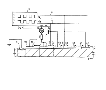
Fig. 3 shows an embodiment of a device according
to the invention. In contrast with the device shown in Fig.1,
the input stage 12 is now connected not only to the signal
source 13, which supplies the input signal Vin, but also to
a reference voltage, in this case earth, via the field effect
PHN.11.711 6 16.12.86
transistor 20 acting as a switch. The remaining parts of the
device are provided with the same reference numerals as in
the device shown in Fi~. 1 for the sake of simplicity.
The transistor 20, whose channel is of the n-conductivity
6 type, just like the channel 3, is controlled by the clock
voltage ~1' which is also applied to the adjacent clock
electrode 4. Consequently, the transistor 20 i9 activated
at the same instant at which the clock electrodes 4 are
activated, as a result of which the input gate 12 is connected
to earthr The operation of the device is explained with
reference to Fig.4. Corresponding potential levels are
provided in this Figure again with the same reference numerals
as in Fig. 2. The maximum and minimum values of Vin again
correspond to the potential levels 18 and 18', respectively,
in Fig. 4. As is shown in the drawing, it is now possible
again that the level 18 lies below the potential level 17a,
which with the applied clock voltage of 5 V is the lowest
potential level that can be attained below the transfer
part 4a. There can be started from the situation in which
~1 = V and ~2 = 5 V corresponding to the potential levels
17'a,17'b below the clock electrode 4 and to the potential
levels 16b and 16a below the sample electrode 11b,11a. If an
input signal Vin is supplied, this value for Vin is applied,
because the switch 20 is non-conducting, to the input gate,
as a result of which the surface potential below this gate
corresponds in the absence of charge to the level 18.
Subsequently, ~1 rises to 5 V, while ~2 falls to 0 ~. Below
the sample gate 11b,11a, the potential barrier 16'b,16'a is
formed, which insulates the charge packets below the input
gate 12 and the input diode 10 from each other. Below the
first clock electrode 4, the potential well 17b is induced,
while the barrier 17'a is reduced to the level 17a.The major
partof the charge packet above the level 18 would already
be transerred to the potential well 17b. However, at the
same time, the transistor 20 is activated, as a result of
which the earth potential is applied to the input gate 12.
This results in that the potential level below the input
gate 12 rises to the level 18", which is indicated in the
PHN. 11.711 7 16.12~86
drawing by a broken line. Due to the fact that the level 18"
lies above the level 17a, the whole charge packet Eormed
below the input gate 12 will be transferred. At a next stage,
~1 returns to 0 ~, as a result of which the potential
5 barrier 17a is increased again to 17'a. Simultaneously, the
transistor 20 becomes non-conducting, as a result of which
the input signal Vin can be applied a~ain to the input gate
12 and a new charge pack.et can be formed.
For a satisfactory operation of the device des-
cribed here, it is necessary that the impedance Z, which may
form part of the signal source 13, is higher than the internal
impedance of the switch 20 in the closed condition. Fig. 5
shows for a digital application, by way of example, the
circuit diagram of a signal source 13 having an internal
lS impedance Z which can be adjusted to a suitable value in a
simple manner~ The circuit comprises two field effect
transistors 22,23, whose source zones are applied to a
voltage V1 corresponding to a logic "1" and to V0 corres-
ponding to a logic "0" respectively. The drain zones are
connected to the input gate 12 shown diagrammatically.
For the sake of clarity, the switching transistor 20 is also
shown in the drawing. The information IN is supplied to the
input of an amplifier 24, of which the output is directly
coupled to the gate of the transistor 22 and via an inverter
stage 25 to the gate of the transistor 23. In the case in
which IN = 1, the transistor 22 is conducting and the voltage
V1 is applied to the input gate 12.Inthe other case, in which
IN = 0, the transistor 23 is conducting and the voltage V0
is applied to the input gate 12. For the impedance Z,
simply the resistor of the transistors 22,23 can be used.
The said resistor can be adjusted to a suitable value,
for e~ample, by choosing the W/L ratio ~ratio channel width
to channel length).
It will be appreciated that the invention is not
limited to the embodiment shown here, but that many varia~ons
are possible for those skilled in the art within the scope
of the invention. For example, the device described here with
PHN.11.711 8 16.12.86
incorporated potential barrier may also be operated as a
known one-bit per electrode device, in which there is in
a group of successive filled storage sites only one vacancy,
which is displaced through the charge transport channel in
the direction opposite to the charge transport direction.
The invention may also be used in known three- or four-phase
CCD's without incorporated potential barrier.