Note: Descriptions are shown in the official language in which they were submitted.
5~3
INTEGRATABLE MICROWAVE DEVICES BASED ON FERROMAGNETIC FILMS
DISPOSED ON DIELECTRIC SUBSTRATES
Background of the Invention
This invention relates generally to microwave devices
and more particularly to microwave magnetically tuned devices
which can be integrated with microwave monolithic integrated
circuits.
As is known in the art, so-called monolithic microwave, and
millimeter wave integrated circuits include active and passive
devices which are formed using semiconductor integration
circuit techniques to provide various types of microwave and
millimeter wave circuits. In particular, monolithic microwave
integrated circuits which include field effect transistors,
transmission lines, resistors, and capacitors may be inter-
connected to provide various microwave circuits such as
amplifiers, filters, switches, and the like. Such monolithic
microwave integrated circuits are generally fabricated on
materials such as gallium arsenide which have generally
accepted characteristics which make their performance suitable
at microwave frequencies.
Two types of microwave devices which are commonly employed
in the art are so-called band reject filters and switches.
Band reject filters, are frequently used in electronic
counter measurement systems (ECM), as well as, electronic
support measures systems (ESM), particularly in receiver
~g
;,
~9~5~7~
channels to suppress a strong signal in a certain frequency
band, when it is desired to detect and process other signals
particularly weaker signals located in adjacent frequency
bands. Such filters are also commonly employed in certain
radar systems to isolate the radar receiver path from a
transmitted signal during radar transmission particularly
when the transmi~ter and receiver share a common signal path.
Commonly, a tuneable band pass filter is employed in such
radar systems and during transmission it is detuned from the
frequency of the transmitted signal~
Generally, the filters described above include YIG-sphere
resonators that are tuned by means of an externally applied
magnetic field. Several disadvantages occur with the use of
YIG tuned resonators. A significant disadvantage is that
although YIG filters have been built using photolithographic
techniques, the requirement of the orientated YIG sphere, as
well as, difficulty with electromagnetic coupling to the
sphere make such magnetically tuneable devices based
upon YIG sphere resonators not readily integratable with
semiconductor circuits. Furthermore, if the filter has to
operate at relatively high microwave or millimeter wave
frequencies typically above 20 GHz, ~or example, a very large
magnetic field is required to provide the requisite resonant
circuit. At 20 GHz, it becomes very difficult to provide a
large magnetic field in a package of small, acceptable size
in applications where size is important.
- 2
~9~S~7~
Accordingly, a magnetically tuned circuit which may be
fabricated using semiconductor integration circuit techniques
and which may be directly integrated with such integrated
circuits would be desirable. Further, circuits which operate
at lower magnetic field strengths and which are also compact
would also be desirable.
~2S~IL57B
62gOl-~36
Summary of the Invention
In accorclance with the present lnvention, there ls
provided a microwave circuit element, comprisiny: a dielectric
substrate; a ground plane conductor disposecl over a first surface
of said substrate; a patterned composite strip conductor disposed
over a second opposing surface sald substrate, said patterned
composite strip conductor, comprisiny: a first layer comprising a
magnetic material disposed on said substrate and having a pair of
easy axes disposed in the plane of said second opposing surface of
said substrate; a second layer of a conductive nonmagnetic
material disposed over said layer of magnetic material; means for
providing a magnetic field parallel to at least a portion of said
pattern composite strip conductor; and wherein said patterned,
composite conductor is disposed parallel to one of the easy axes
of said magnetic material.
With this arrangement, a tuneable band reject filter is
provided. The ferromagnetic material has a ferromaynetic resonant
frequency which is related to the anisotropic field, the
saturation magnetization and the gyromaynetic ratio of the
ferromagnetic film. ~ sicJnal fed to this circuit will pass
through substantlally unattenuated unless the siynal has a
frequency related to the ferromagnetlc resonant frequency of the
materlal. Signals having a frecluency in the vlcinlty of the
ferromagnetic frequency will be absorbed by the clrcuit. Thus,
the clrcult acts as a band stop or band reject fllter. If a DC
maynetlc field is disposed parallel to the direction of the
propagation of the signal, the DC magnetic field will provide a
9~57~3
62901-73
corresponding change in the resonant frequancy of the
ferromagnetic ma~erial. This arrangement provides a tuneable band
reject or band stop filter. Furthermore, i~ an external DC
magnetic field is
~a
provided normal to the direction of propagation and in the
plane of the ferromagnetic layer, the ferromagnetic resonance
mode is not excited and, therefore, there is substantially no
attenuation of the signal fed to the circuit. By switching
the DC magnetization from an orientation parallel to the
direction of propagation to an orientation normal to the
direction of propagation, the above described structure can also
be used as a switch that has a broadband low insertion loss in
one state and a relatively narrow band high absorption in the
opposite state, and thus a switched, band reject filter is
provided.
In accordance with a further aspect of the present
invention, a band reject filter comprises a cubic single
crystalline substrate having a surface of (lOO) faces. A
patterned, composite strip conductor disposed on said (100)
surface comprising a first layer of a crystalline ferromagnetic
material having a pair of easy axes which lie in the plane of
said (lOO) surface and a second layer disposed over said first
layer comprising a conductive nonmagnetic material with said
second layer and first underlying layer, each disposed with
respect to said (lOO) orientated substrate surface, such that
the propagation direction along the patterned composite strip
conductor is parallel to one oE easy axes of said first layer
of magnetic material. With this particular arrangement,
by using the surface of a ~lOO) substrate and by depositing a
ferromagnetic film on this ~100) surface having a pair of
easy axes disposed in the plane of the (100) surface, a DC
magnetic field applied parallel to the propagation direction
along the composite conductor will permit the fre~uency at
which the band reject filter has a maximal insertion loss
(i.e. when the ferromagnetic layer is at resonant and hence,
absorption is at a maximum) to be adjusted since it is dependent
upon the externally supplied magnetic field thus providing a
tuneable band stop filter.
In accordance with a further aspect of the present
invention, a r.f. switch includes a cubic single-crystal
substrate having a (100) surface and a patterned composite
strip conductor disposed over said (100) surface, said composite
strip conductor includes a first layer comprised of a magnetic
material having a pair of easy axes which lie in the plane of
said (100~ surface~ The layer of magnetic material has first
and second strip portions which have a common terminus and
which are disposed orthogonal to one another in the common
plane of said (100) surface. The first and second strip
portions are disposed parallel to respective ones of said
easy axes of said magnetic material. The composite strip
conductor further includes a second layer of a conductive,
non-magnetic material having first and second mutually orthogonal
portions having a common terminus and disposed over said
first and second magnetic strip portions, and a third portion
S7~3
connected at the terminus of said first and second portions,
and disposed on said substrate~ With this particular arrangement,
a single pole, double-throw r.f. switch is provided. A
microwave signal entering the input i.e. the third strip
conductor por~ion is split in half with no energy being
re~lected. I the ferromagnetic material disposed under the
two branches of the strip conductor is màgnetized uniformly
in either the ~ 010> or the ~001> directions, one of the
output branches will have a higher attentuation than the
other output branch due to the excitation of ferromagnetic
resonance at a certain frequency band. Thus, the structure
acts as a single pole, double-throw switch having broadband
low insertion loss in one state (i.e. in which the ferromagnetic
resonance is not excited) and narrowband high absorption as
in the other state (i.e. in which the ferromagnetic resonance
is excited).
In accordance with a still further aspect of the present
invention, a small electromagnet suitable for use to provid0
an external D.C. magnetic field to the tuneable circuits
includes a substrate comprised of a ferrite material, said
substrate having four salients thereon with a coil disposed
around each of said salients. Alternatively, a pair of coils
are provided about the substrate with each coil disposed
around a pair of opposing edges of said substrate. With such
an arrangement, in response to currents of suitable polarities
-- 7 --
~Z~78
fed to the coils, an electromagnetic having a pair o~ mutually
orthogonal magnetization directions is provided,
~ . - 8 -
~g9~578
Brief Description of the Drawings
The foregoing features of this invention, as well as
the invention itself, may be more fully understood from the
following detailed description of the drawings, in which:
FIG. 1 is a block diagram of a radar having a switchable/
tuneable band reject filter disposed to block leakage of a
transmitted signal into a receiver;
~IG. 2 is an isometric view of a band reject filter
in accordance with a first aspect of the present invention;
FIG. 3 is a plot of attenuation (in db) versus frequency
(GHz) for various thicknesses of a ferromagnetic film used in
the device of FIG. 2;
FIG. 4A and 4B are plo~s of attentuation versus frequency
for various values of DC magnetic field oriented parallel
with respect to propagation direction along the device of
FIG. ~;
FIG. 5 is a plot of attenutation (db) versus frequency
for different electrical conductivities of the ferromagnetic
material;
FIGS. 6A-6D are a series of isometric views showing
steps in construction of a ferromagnetic film with an
effective electrical conductivity smaller than the bulk
conductivity of the material;
FIG. 7 is a plan view of a meandered strip conductor
band reject filter with a diagram showing conductor orientation
with respect to crystalline axes in accordance with a further
aspect of the present invention;
_ g _
~2~
FIG. 7~ is a cross-sectional view taken along lines
7A-7A of FIG. 7;
FIG. 8 is a cross-sectional view of a further embodiment
of a band reject filter having a high degree of attenuation;
FIG. 9A is a plan view of a single pole, double throw
switch having a ferromagnetic material as a switching element
with a diagram showing conductor orientation with respect to
crystalline axes in accordance with a still further aspect of
the present invention;
FIG. 9B is a cross-sectional view taken along lines
9B-9B of FIG. 9A;
FIG. lO is an isometric view of an electromagnetic assembly
useful to provide the external magnetic field for the device
as shown in FIGS. 2, 7, and 8;
FIG. ll is an isometric view of an alternate design for
a magnet assembly for use with the circuit shown in FIGS. 2,
7, and 8;
FIG. 12 is a composite isometric view showing a further
alternate embodiment of an electromagnet disposed on the band
reject filter of FIG. 7; and
FIG. 13 is a schematic diagram of an electrical circuit
used with the electromagnet shown in FIG. 12.
-- 10 --
~?~9~57l 3
Descript_on of the Preferred Embodiments
Referring now to FIG. 1, a typical radar system 10 is
shown to include an antenna 12 coupled to a duplexer 14. A
first port of duplexer 14 is connected to a first path via a
transmitter 16, and a second port o duplexer 14 is coupled
to a receiver 18 via a band stop filter 20, as shown. A
control circuit 19 is fed a signal, via path 16a, from the
transmitter 16 to provide a signal, via path l9a, to the band
stop filter 20 to switch the band stop filter 20 between a
pair of states. In the first state, the band stop filter
will be switched to stop or prevent passing of signals having
a frequency corresponding to the frequency of the transmitted
signal from transmitter 16 (i.e. during a transmit mode) as
may occur because of leakage of the signal through the duplexer
14; whereas in a second state, the band stop filter will
permit without significant attenuation signals to be coupled
from antenna 12 to the receiver 18 (i.e. during a receive
mode). Preferred embodiments of the band stop filter 20 will
now be described in conjunction with FIGS. 2-8.
Referring first to FIG. 2, a band stop filter 20 is shown
to include a substrate 22 here comprised of a dielectric or
semiconductor material such as gallium arsenide having a
surface 22a of tlOO) crystalline planes or faces, having
disposed over surface 22a, a composite strip conductor 26
comprised of a first layer of an electrically conductive
-- 11 --
~L?.91~
magnetic material 27 such as a layer comprised of iron (Fe)
and a second layer 28 of an electrically conductive, non magnetic
material. Layer 27 is arranged on said substrate 22 such
that the easy axes of the crystal structure of said layer 27
are disposed in the plane of the substrate surface 22a with
the easy axes being aligned with the ~ 010 ~ and ~ 001>
directions of the substrate 22. Disposed over and here on
said iron layer 27 is the conductive layer 2~ here of a
highly conductive material such as gold. Typically, the
layer of iron will have a thickness in the range of about
0.01 micrometers to 0.3 micrometers with 0.1 micrometers
being a typically preferred value. Typically, the thickness
of conductive layer 28 will be at least twice the thickness
of the iron layer 27.
The arrangement shown in FIG. 2 provides a simple band
stop or band reject filter 20. It is generally preferred that
the width W26 of the composite strip conductor 26 is chosen in
conjunction with the thickness of the dielectric substrate 22 to
provide the microstip transmission line media with a desired
characteristic impedance here 50 ohms. Since the orientation
of the composite strip conductor 26 with respect to the
crystalline axes of the gallium arsenide substrate is chosen
such that the microstrip line is parallel to a selected one
o the in-plane "easy axis" of the Fe film, (that is either
the C 010> or ~ 001~ axis), when a DC magnetic field is applied
parallel to the microstrip conductor as shown in FIG. 2 the
- 12 -
s~
strength of this field will determine the frequency at which
the microstrip conductor has a maximal ferromagnetic absorption.
For a thin film as shown in FIG. 2, the ferromagnetic frequency
(fres) is related to the applied magnetic field H, the anisotropy
field Han, the saturation magnetization 4 Ms and the gyromagnetic
ratio ~ by the equation:
2 ~ fres y ~(H+Han)(H~Han+4~r Ms)} 1/2 Equation 1
For an iron film at room temperature 4 ~ MS = 22,000 Oe;
Han 550 Oe; and y/2~ = 2.8 MHz/Oe. This implies that for
H=0 the resonant frequency of the structure shown in FIG. 2
is approximately 9.86 GHz.
The transmission characteristics of a microstrip line
such as shown in FIG. 2 have been analyzed by approximating
it as a parallel-plate transmission line. This analysis
takes the gyromagnetic properties and the electrical conductivity
of the Fe film accurately into account, but is approximate
insofar as it assumes that the ground plane and the metal
strip covering the Fe film are perfect conductors (infinite
conductivity).
The magnetic properties of the magnetic film are
characterized by a permeability tensor of the form:
_j O` i
_ j 0 Equation 2
O 0
~9~S7~3
The components J~ and ~ of this tensor can be derived from
the Landau-Lifshitz equations (with damping included) and
are given by:
(fH~i ~f~ / ~(fH+j ~f)2 _ ~2 ~
~ = _fMf / ~(fH+; ~ f)2 _ f2} Equation 3
where ~ is a phenomenological damping parameter, which is
numerically approximately 0.004 for Fe (inferred from line-
width measurements on Fe~ilms at Ka-band)~ The "effective"
permeability is given by
2_R2) /~ Equation 4
1 + fM(fH+fM+i~ f) / ~(fH~i~ f~(fH+fM+i~ f) f
In Eqs. (3) and (4) fH and fM are given by
2 ~fH = ~'(H+Han)
2~ fM = ~ (4l~MS) Equation 5
Here some of the results of an analysis of wave propagation
relevant to the operation of the band-reject filter are
summarized. Figures 3 and 5 show the calculated attenuation
per unit length of microstrip (in dB/cm) as function of
frequency. In all cases the saturation magnetization and
the anisotropy field are assumed to have the values appropriate
for Fe (4 ~Ms 22000 Oe, Ha~550 Oe~, the dielectric constant
of the substrate is assumed to be 10 and the substrate thickness
is assumed to be 100 ~m ( 0.004"). Dielectric losses in
the GaAs substrate are neglected. Magnetic losses in the
1?~91578
Fe-film are taken into account by means oE the "Landau-Lifshitz"
damping parameter ~ .
Figure 3 shows the calculated attenuation per unit length
(in dB/cm) for Fe films of different thicknesses when no
S magnetic field is applied (but the film is magnetized in a
direction parallel to the microstrip). In FIG. 3, curves 21a
through 21d correspond to respective thicknesses of 0.01 ~ m,
0.03 ~ m, 0.1 ~ m, and 0.3 ~ m. As expected from Eq. (1)
resonance absorption occurs at approx. 9.86 GHz in this case.
The height of the peak increases with film thickness when
the thickness is very small, but then saturates due to the
skin effect,
The skindepth at and near resonance is much smaller than
would be expected in a non--magnetic metal of the same
conductivity. In a non-magnetic metal the skindepth ( ~ )
can be expressed as
/ ~ = / 1 Equation 6
~non mag ~ O ~ O
where ~ is the conductivity and ~ O the permeability of
vacuum. Using the conductivity of Fe(l/~ = 8.85xlo-8 ohm m),
one finds Eor f=10 GHz
~ non mag ~ 1.50 ~ m Equation 7
In the present context it is convenient to characterize the
electrical conductivity O~ by a frequency fc according to5
fc = ~ o Equation 8
- 15 -
9~L5713
For Fe this frequency is approx. 2xlo8 GHz. Equation (6) for
the skindepth in a non-magnetic metal can be expressed in
terms of fc as
~ = c~ ~ Equation 9
non mag 2~ f fc
where cO is the velocity o light in vacuum.
This formula is not applicable in a ferromagnetic metal (and
especially not at FMR) because it does not take lnto considera-
tion the large permeability at ferromagnetic resonance. The
correct formula for the skindepth at resonance can be shown
to be
Sres = ~ ~ ~ Equation 10
Here the last factor is usually very close to unity, and can
therefore be neglected. For Fe using the numerical values
given above, one finds
Sres ~ 0.028 ~ m Equation 11
i.e., a more than 50 times reduction of the skindepth compared
to Eq. (7).
From four curves (21a-21d) shown in FIG. 3 which are
applicable to film thicknesses of 0.01 ~ m, 0.03 ~ m, 0.1~ m,
and 0.3~m, it becomes readily apparent that saturation of
the attenuation sets in near 0.03 ~ m as expected on the
basis of Eq. (11?.
- 16 -
s~
Referring now to FIGS. 4A and 4B, calculated plots
23a-23h of attenuation per unit length as a function of
frequency at different field strengths between H=0 to H--5400
Oe. are shown. In FIG. ~, curves 23a-23d the external Eield
H is varied in 100 Oe steps from H=0 curve 23a to H=300 curve
23d. In FIG. 4B, H is varied in 200 Oe steps from H=4800 Oe
(curve 23e) to H=5400 Oe (curve 23b). These calculations
assume a substrate thickness of 100 micrometers, a film
thickness of 0.03 micrometers, dielectric constant for the
substrate of 10, saturation magnetization (4 TrMs) 22,000 Oe,
an anisotropy field Han = 550 Oet Fc = 2X10⁸ ~Hz, and ~ =
0.004. As shown, by increasing the external magnetic field,
the stop band of the filter increases accordingly from
approximately 9.86 GHz up through 36.2 GHz as shown for
H=5400 Oe (curve 23n). Accordingly, a magnetically tuneable
band stop filter is provided with this arrangement. FIGS.
4A-4B also sho~ that the attenuation peaks can be tuned to
relatively high frequencies with application of a relatively
small external magnetic field. This compares favorably with
the field requirements of YIG resonators.
In the calculations above, it is assumed that the
electrical conductivity ( Gr ) is equal to 1/8.85 X 10-8
ohm meters, which is the accepted value of ( o-) for bulk
iron at ~oom temperature. In practice, it is felt that in
thin Fe films, the effective conductivity may be considerably
- 17 -
57~3
smaller due to increase scattering of carriers at the film
surfacesO Since attenuation per unit length is related to
the conductivity of the nonmagnetic film, it is anticipated
that the actual attenuation per unit length will be even
greater than that shown above.
Referring briefly to FIG. 5, FIG. 5 shows the attenuation
per unit length as a function of frequency for four values of
the frequency term fc which is directly porportional to the
conductivity (or). In FIG. 5, curves 25a-2Sd represent values of
Ec equal to 2.0X10⁸ GHz; l.OX108 GHz, and 0.2X10⁸ GHz. With
decreasing conductivity (curve 25a to curve 25d), the peak
attenuation increases significantly. As characterized by the
frequency fc~ when fc is equal to 2X10⁸ GHz (which corresponds
to using a conductivity of the accepted bulk conductivity
value~, it is approximately 12 dB per cm at 9.86 GHz. Using
a frequency fc which is 0.2X10⁸ GHz shows an attenuation of
approximately 28.5 dB per cm. Therefore, when the conductivity
is decreased by a factor of 10 relative to the bulk conductivity
of iron, the attenuation increases significantly from about
12 dB per cm to approximately 28.5 dB per cm.
Referring now to FIGS. 6A-6D, steps in the fabrication
of a band stop filter 20' (FIG. 6D) having an epitaxial iron
layer having an electrical conductivity substantially lower
than bulk conductivity for iron will be described.
- 18 -
157~
Referring first to FIG. 6A, substrate 22 has the ground
plane 24 disposed over a first surface thereof, and is provided
with a thin film of iron 34 over surface 22a having the
thickness as selected above in conjunction with FIG. 2. The
thin film of iron 34 is covered by a masking layer 35 which
is patterned to provide a mask (not shown) which exposes
selected underlying portions of the iron layer 34. As shown
in FIG. 6B, the iron layer 34 is then etched away in the
exposed portions to provide strips 34a spaced by thin grooves
37 disposed perpendicular to the direction of propagation of
the microstrip conductor which will be fabricated later.
As also shown in FIG. 6B, after the grooves 34a are etched
into the Fe film as by conventional chemical etching, the
masking layer 35 is removed and the strip~ 34a of the Fe
layer and the grooves 37 are covered with a thin insulating
layer 38 of a material such as silicon oxide.
As shown in FIG. 6C~ the insulating film 38 having
disposed thereunder the patterned Fe layer 36 is covered with
a relatively thick layer 39 of a conductive material such as
aluminum or gold. As shown in FIG. 6D, the grooved Fe film
and conductive layer 39 are then patterned to provide the
microstrip strip conductor with a selected width and length
as in FIG. 2 to provide band stop filter 20'.
The effective electrical conductivity of the Fe film 34 for
the arrangement shown in FIG. 6D will be substantially less
-- 19 --
7 ~
than the effective electrical conductivity of the Fe layer 27
shown in FIG. 2 because the path of current flow in the Fe layer
27 is interrupted by the insulating layer 38, whereas the
insulating layer 38 allows the magnetic field of the signal
fed to the conductor 39 to interact with the ferromagnetic
Fe layer 34.
Referring now to FIGS~ 7 and 7A, a compact band stop
filter 20'' having a high attenuation per unit length is shown
to include a composite meandered strip conductor 42 including
a Fe film 44 having an effective conductivity which is equal
to bulk Fe conductivity disposed on the GaAs substrate 22 and
a conductive, non-magnetic layer 43 diposed over the Fe layer
44. The meandered strip conductor 42 has long leg portions
42a which are disposed parallel to one of the in-plane easy axes
of the Fe film as generally described earlier and a plurality
of short legs 42b which are disposed parallel to a second one
of the in-plane directions of the Fe film and orthogonal to
the long leg portions 42a. The meandered (i.e. multiple
folded) strip conductor 42 provides a band strip filter which
occupies a substantially smaller area to provide a selected
attenuation per unit length than if the device were provided
as a single long strip conductor.
It may be further understood that the iron film having
r0duced bulk conductivity as described in FIG. 6 may be used
with the meandered line shown in FIG. 7 to provide a band
stop filter having an even higher attenuation per unit length.
- 20 -
9~LS~E3
It should now be appreciated that one of the important
considerations in providing a band stop filter is the thickness
of the dielectric spacing between the composite strip conductor
and the ground plane conductor disposed on the gallium arsenide
substrate. In general, the thinner the dielectric the higher
the attenuation per unit length of the band stop fllter.
Accordingly, it is desirable to provide a relatively thin
dielectric spacing between the ground plane conductor and the
composite strip conductor of the band stop filter. Several
techniques accordingly are available for providing such an
arrangement. One technique in particular would be to etch
the gallium arsenide substrate in a region thereof underlying
the Fe layer to provide a tub structure thereunder. A preferred
technique, however, is as shown in FIG. 8.
Referring now to FIG. 8, a band stop filter 20''' is
shown to include here a gallium arsenide substrate 22 having
disposed over A first surface thereof a ground plane conductor
24 and disposed over a second surface thereof a layer of a
magnetic material such as iron as described above. Disposed
over said iron layer 57 is a dielectric layer 58 comprised of
a material such as silicon nitride (Si3N4) or silicon dioxide
(SiO2). The dielectric layer 58 is provided to have a selected,
controlled thickness generally in the order of about l micron.
Disposed over the dielectric layer 58 is a conductive layer
59 which is patterned to provide in combination with the dielectric
~?a~9~i7~3
58 and iron layer 57 a microstrip transmission line having a
selected characteristic impedance. Since the dielectric for
the microstrip transmission line is provided by the relatively
thin dielectric layer 58 and further since the ground plane
conductor for the microstrip transmission line is provided by
the iron layer 57, generally the width of the conductive
layer 59 would be about 1/10 width o the iron layer 57.
Further, since the iron layer 57 must be electrically connected
to the ground plane conductor 22, via holes 60 are here
disposed through the substrate 22 to provide electrical
connection between the ground plane conductor 24 and the iron
layer 57. Preferably, such via holes 60 are provided at the
input and output terminals of the bandpass filter. Alternate
arrangements such as the use of coplanar waveguide at inputs
and outputs of the filter may be used. Since the attenuation
per unit length is a function of the dielectric separation
between the strip conductors and the ground plane conductor,
the arrangement described in conjunction with FIG. 8 will
provide a band stop filter having significantly higher
attenuation per unit length.
~eferring now to FIGS. gA and sa, an alternate embodiment
of the present invention is shown. Here a single-pole,
double-throw switch 50 is disposed on a substrate 22
having a ground plane conductor 24 disposed thereover as
generally described in conjunction with FIG. 2. Here a pair
- 22 -
~l~9~7~
of composite strip conductor sections are disposed m~tually
orthogonal to one another and parallel to the pair of e~sy
axis of the ~allium arsenide substrate 22. A third leg of
said single pole, double-throw switch 50 comprised of a single
layer of a conductive non-magnetic material such as gold is
disposed on substrate surface 22a opposite the intersection
of the pair of orthogonal composite strip conductors 52b and
52c, as shown. The device described in conjunction with
FIGS. 9A and 9B when magnetized in one of its "easy directionsl',
provides a single-pole, double-throw switch which has a
broadband low insertion loss characteristic in one branch and
a relatively narrow-band high absorption characteristic in
the other branch. The branch in which the direction of
magnetization is normal to the propagation direction has a
low insertion loss, whereas the branch in which the direction
of magnetization is parallel to the propagation direction has
a high insertion loss. Here, the characteristic impedance of
the input microstrip line shown in FI~. 9A is chosen to be
half of the characteristic impedance of the output lines; and
therefore, the energy of a wave entering the junction from
the input side will be split in half with no energy being
reflected. If the Fe film is magnetized uniformly in either
the C 010~ or the ~ 001~ directions, one of the output branches
will have a much higher attenuation than the other due to the
excitation of ferromagnetic resonance at a certain frequency.
~9~578
Therefore, the structure shown in FIG. 9A acts as a single
pole, double-throw switch.
Moreover, the structure shown in FIG. 2 may also be used
as a switch. As described in conjunction with FIG. 2, the
attenuation applies only to the band stop filter when the DC
magnetic moment is parallel to the microstrip transmission
line. Another stable orientation of the DC magnetic moment
is perpendicular to the microstrip transmission line. In
this latter orientation, the ferromagnetic resonance is not
excited because the r.f. magnetic field is substantially
parallel to the DC magnetization; and therefore, the structure
shown in FIG. 2 can also be used as an on/off switch that has
a broadband low insertion loss in one state and relatively
narrow band high insertion absorption in the other state.
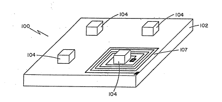
Referring now to FIG. 10, a small electromagnet lO0 suitable
for use for the band stop filter shown for example in FIG. 7
is shown to include a substrate 102 comprised of a ferrite
such as Li-ferrite or Li-Zn ferrite having four salients 104
disposed over an upper surface thereof and photo etched coils 107
disposed around each one of the salients 104, ~only one being
shown). The photo etched coils 107 provide in combination
with the ferrite plate 102 an electromagnet. By providing a
current through each one of the coils with one of two possible
polarities, a maynetic field can be generated near the center
of the plate 102. In particular, the magnetic field direction
- 24 -
~s~s~a
can be varied from being parallel to a first set of opposing
plate edges to being parallel to a second, different set o:E
opposing plate edges, and thus orthogonal to the first set of
plate edges. This is accomplished by simply changing the
polarity of the current directed through each one of the
coils. Therefore, the electromagnet illustrated in FIG. 10
can generate a magnetic field that has a pair of directions
required for switching a band reject filter, as well as, for
the single pole, double-throw switch as described in conjunction
with FIGS. 2-9B above~
An estimate of the strength of the magnetic field which
can be generated by the electromagnet shown in FIG. 10 is given
below:
In order to estimate the strength of the magnetic field
that can be generated by the electromagnet shown in FIG. 10,
consider the example summarized in Table 1. Assume also that
the voltage applied to the coil is 24 volts. Since the
resistance is 144 Ohm the current is I=1/6 Amp and the power
dissipated (per coil) P=4 Watt. The heat generated in the
coil can be removed by means of a metal block (not shown)
with cooling fins, which is bonded to the back of the ferrite
plate.
- 25 -
571S
Table 1
Typical Parameters for Small Electromagnets
Such as Shown in Figure 9
Overall size of electromagnet 5 mm x 5 mm x 1.5 mm
Width of each salient 0.5 mm
Width of conductors 10 ~ m
Height of conductors 5 ~ m
Spacing between conductors 10 ~ m
Length of conductor (each coil) 0.3 m
Number of turns (each coil) 50
Resistance (each coil)
(assuming ~ = 2.4x10⁻⁸ Ohm m) 144 Ohm
The magnetic fieldstrength generated at the center of
the electromagnet is approximately given by
~ TN
H ~ D (1)
where I is the current, N the number of turns and D the
pole-to-pole distance. Since D=2 mm in the example of
Table 1, the estimated fieldstrength is
H ~ ~n ~ = 41.67 cm = 52.36 oersted (2)
Assuming that the coercivity of the Fe films is approx.
6 Oersted, the field generated by the coil is therefore more
than adequate to switch the magnetization from one easy
direction to another.
- 26 -
L571~
Referring now to FIG. 11, an alternate embodiment 110'
for a small electromagnet suitable for use with the switcheable
band reject Eilters 20'-20''' and switch 50 is shown. This
electromagnet includes a substrate 112 comprised o a magnetic
S material having a high permeability such as a ferrite or a
nickel iron alloy which is machined to have octagonal configura-
tion with four salients 114 disposed within and protruding from
the walls of the octagonal shaped substrate 112 as shown.
Wires 107a and 107b are coiled about pairs of opposing surfaces
of the octagonal shaped substrate 112 to form first and
second magnetic circuits, as also shown. For optimum performance,
both circuits are activated at the same time and depending
upon the polarity of the currents fed to each of the coils,
the resulting ~agnetic field near the center of the structure
will be either in a direction from pole 1 to pole 3 or in a
direction from pole 2 to pole 4; and thus, the electromagnet
110 shown in FIG~ 10 also can generate a pair of magnetic
fields having the directions re~uired for the switcheable
bandpass filter, band stop filter (FIG. 2), and a single
pole, double-throw switch 50 (FIG. 9).
Referring now to FIG. 12, a further alternate embodiment
60 for a small electromagnet suitable for use with the
switcheable band stop filter described in conjunction with
FIG. 7 in particular is shown. Here the electromagnet 60
includes a semi-toroidal shaped member 62 having
- 27 -
~?g9~7~3
leg portions 62a, 62b disposed from a base portion 62c all
comprised of a high permeability magnetic material. The
semi-toroidal member 62 has regions 63a, 63b removed which
will permit the toroidal member to be mounted on the substrate
22 of the band stop filter in such a manner that the toroid
62 does not electrically interfere with the meandered strip
conductor ~2. A coil of wire 64 (one turn shown) is wound
about the base portion 62c and the electromagnet is disposed
over the meandered strip line 42, onto substrate 24 as shown.
Here onl~ a single turn is shown although several turns
obviously would be provided in order to increase the field
strength. This coil of wire 64 is fed by a current and the
semi-toroidal assembly 62 is used to provide a field which is
parallel to the long branches of the meandered line.
lS Referring now to FIG. 13, a schematic diagram of an
electrical circuit 70 used to generate an external magnetic
field is shown. The circuit 70 includes a switch 72 which
is used to selectively couple a current pulse from a source 74
through the meandered line 42 (Fig 7) and a pair of high pass
filters 76a, 76b used to block the current pulses ~rom the
remainder of the system within which the band pass filter 20''
tFig 7) is disposed. The high pass filters 76a, 76b are here
provided by D~C. blocking capacitors. Circuit 70 also includes
a pair of low pass filters 78a, 78b, here inductors to provide
a low impedance path for the current pulse from the switch to
ground through the meandered line 42. A current directed
- 28 -
9~;7~
through the meandered line ~2 (FIG. 7) provides in response
thereto a magnetic field perpendicular to the meandered line.
This field is substantially orthogonal to the magnetic field
generated by the external electromagnet described in conjunction
with FIG. 12. The current directed through the meandered
line which is an integral part of the bandpass filter produces
a magnetic field perpendicular to this line whereas, the
external electromagnet (FIG. 12) provides the required magnetic
field parallel to the long branches of the meandered line.
This arrangement has two particular advantages: One advantage
is that in a low absorption state (i.e. where the D.C. current
is directed through the line by the circuit o~ FIG. 13) of
the switcheable band stop filter, the magnetization o~ the Fe
film is everywhere perpendicular to the meandered line not
just in the long branches of this line as in the approaches
in FIGS. 10 and 11. Thus, the insertion loss in the low
absorption state is expected to be substantially lower for a
filter using the electromagnet shown in FIGS. 12 and 13 than
for a filter using the electromagnet shown in FIGS. 10 or 11.
Secondly, since the external electromagnet shown at FIG. 12
is used exclusively for generating the magnetic field parallel
to the microstrip lines, it can be designed to achieve an
optimum or higher field strength than the electromagnet shown
in FIGS. 10 and 11. This would indicate that the structure
shown in FIG. 12 will have a greater tuneability range than
those described in conJunction wlth FIGS. 10 and 11.
- 29 -
ii7~
Each of the circuits described above have been shown
with a conductive layer disposed symmetrically over the
ferromagnetic material. This arrangement in general provides
a reciprocal device. However, it is believed that a non-reciprocal
device would be provided if the conductive layer is disposed
to one side of a ferromagnetic material layer, such that the
conductive layer i5 no longer symmetrically disposed with
respect to the ferromagnetic material~
Having described preferred embodiments of the invention,
it will now become apparent to one of skill in the art
that other embodiments incorporating their concepts may be
used. It is felt, therefore, that these embodiments should
not be limited to disclosed embodiments, but rather should
be limited only by the spirit and scope of the appended
lS claims.
- 30 -