Note: Descriptions are shown in the official language in which they were submitted.
P-87,2450 ~ 9~ ~Z
ENCODING METHOD AND APPARATUS FOR RECORDING DATA WITH
AN IDENTIFIGATION CODE AND AN ER~OR CHECK CODE
BACKGROUND OF THE INVENTION
Field of the Invention
The invention relates to an encoding method and
apparatus suited for recording digital data such as a
digital audio signals.
Description of Prior Art
In a digital tape recorder for recording/reproducing a
digital audio signal with a rotating head, for example, data
iæ recorded on a recording medium to a saturated degree.
For this reason, rewriting the data can be attained without
using an erasing head by recording new data onto already
recorded data directly. However, when the
recording/reproducing operation of data is done with
different apparatuses, there is a possibility that data to
be erased is left as it is due to insufficient compatibility
between those apparatuses.
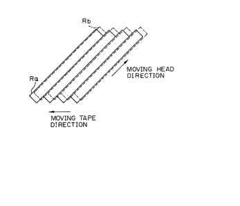
Fig. l shows data recording patterns formed by
overwriting data through a pair of rotatlng heads disposed
at an opposed interval of 180, for example. In Fig. l, a
track Ra indicated by a solid line shows a track formed when
an apparatus A records data, and a track Rb indicated by a
broken line shows a track formed when an apparatus B records
data. This is a case where data recording positions of the
tracks Ra and Rb do not coincide with each other, as shown
in Fig. 1, because of a mechanical variation in the tape
running mechanism between the apparatuses. First, data is
recorded by the apparatus A to from the track Ra. Next,
~:~9~ 2
when new data is recorded on this data by the apparatus B,
an area of the track Ra where the rotating head of the
apparatus B does not scan (area indicated by an oblique line
at B of Fig. 2) is left without being erased. Therefore, if
a magnetic tape having the recording patterns shown in Fig.
1 is reproduced by th0 apparatus A, there is a possibility
that unnecessary data or data (whose) reproduction is not
desired is read out, because the rotating head starts
scanning from an area shown by the oblique line. In the
case where a digital audio signal is recorded/reproduced by
a rotating head, an error detection/error correction code is
usually employed. An example of encoding of the error
detection/error correction is shown in Fig. 3.
In Fig. 3, audio data of (mxn) words and P parity and Q
parity developed from the audio data are arranged in a two-
dimensional fashion. The P parity is formed of n words in a
predetermined direction of data of the two-dimensional
arrangement, for example, in a oblique direction. The Q
parity is formed of n words in another direction of the data
of the two-dimensional arrangement, for instance, in a
column direction. An error detection code such as a CRC
(cyclic redundancy check) code or an error correcting code
such as a Reed-Solomon code is employed to form the
parity. An error check code is formed as data of one block,
on the basis of n-word data disposed in the column direction
of the two-dimensional arrangement data which is composed of
the (mxn)-word data, and the parity (P, Q) and address data
are added to the data of each column. Further, a
synchronization signal is added to the block data and
sequentially recorded on a track of a tape-like recording
medium. As a result, data of m blocks is sequentially
arranged on each track. For the error check code, the error
--2--
check detecting code or the error correcting code can be
used in a manner similar to the P parity and the Q parity.
Meanwhile, the error check code is added to check the
presence of absence of an error of each block, and the block
data is handled as correct data (in the absence of an error
of the block data) even when the block data that should not
be reproduced exists due to the fact that data is left
without being erased. For this reason, if data is read out
of an area in which the data is left without being erased
due to insufficient compatibility between different
apparatuses as mentioned above, the data cannot be detected
as unnecessary data. Consequently, a serious problem
results, in that an abnormal sound is generated. Also,
without being limited to such insufficiency of compatibility
between the apparatuses, the same problem as that mentioned
above is brought about when dust which adhered at the time
of recording is dropped off at the time of partial
reproduction for previously recorded data.
To solve this problem, an adoption of an identification
signal (hereunder called "ID code") as described in the
Japane~e Patent Disclosure No. 1675/1985 laid open to public
inspection has been proposed by the same applicant as the
present application. The ID code ls a binary code of plural
bits, and a predetermined value is allotted to the ID code
for every occurrence of a series of recording data. ~y
monitoring the ID code at the time of reproduction,
undesirable data mistakenly contained with reproduction data
can be detected and eliminated even when no error is found
by the error check code.
Fig. 4 shows an example of a recording format of data
recorded by a rotating head type digital tape recorder. One
block-data length has 288 bits, and an eleven-bit block
--3--
312
synchronization signal comes at the head thereof, a
thirteen-bit block address then appears, and finally parity
(P, Q) of 48 bits (1~ bits x 4 words) for detection and/or
correction of audio data comes next.
16-word audio data Ll, Rl, R2, .... L8, R8 (L: audio
data of left channel, R: audio data of right channel) are
positioned after the parity, and an ID code ID (8 bits) and
a CRC code (16 bits) serving as an error check code ara
added after the audio data. The CRC code performs error
detection of the remaining 261-bit data except the block
synchronization signal.
Also, it can be conceived, as an alternative, that both
of the ID code and the CRC code have twelve bits.
The ID code, which is indicative of a series of
recording, provides high identification capability when an
increased bit number is used, to eliminate the possibility
that there is an accidental coincidence in ID codes between
ob;ective data and data which has not been erased. From
this standpoint, it is desirable that the bit number of the
ID code is made larger.
On the other hand, the probability of erroneous
detection of the error check code becomes lowered with an
increased bit number. Therefore, it is desirable that the
bit number of the error check code be made greater.
However, there is a limitation to redundancy, and it tends
to be difficult to fully secure the bit number of both the
ID code and the error check code.
SUMMARY OF THE INVENTION
An object of the invention is, therefore, to provide an
encoding method and apparatus with improved ID-code
identification capability and error detection capability of
--4--
~,9~
the error check code without increasing redundancy in
recording digital data.
According to one aspect of the invention, there is
provided an encoding method of an identification code and a
first error check code for sequentially recording block
data, hav~ng the identification code and the error check
code, onto a recording medium for every occurrence of a
predetermined number of words, comprising the steps of:
forming the error check code for checking an error
within the predetermined number of words on the basis of
these words;
performing a predetermined operation for the error check
code and for the identification code; and
adding the error check code in which the identification
code is contained inherently through such predetermined
operation to said predetermined number of words.
According to another aspect of the invention, there is
provided an encoding apparatus for encoding an
identlfication code and a first error check code, in
sequentially recording block data, having the codes on a
recording medium for every occurrence of a predetermined
number of words, comprising:
means for forming the error check code for checking of
an error within the predetermined number of words from these
words;
means for performing a predetermined operation for the
error check code and the identification code; and
means for adding the error check code with the
identification code contained therein by said predetermined
operation to the predetermined number of words and
outputting the result.
~?~9~ 2
BRIEF DESCRIPTION OF THE DRAWINGS
The present invention will be apparent from the
following detailed description when taken in conjunction
with the accompanying drawings, in which:
Figs. 1 and 2 show diagrams of data recording patterns;
Fig. 3 shows a diagram of parity generation sequence for
detection and/or correction of a data error;
Fig. 4 shows a diagram of a structure of a data block in
which an ID code and an error check code are added
independently from each other;
Figs. 5 and 9 show diagrams of two structures of block
data to which the present invention is applied;
Figs. 6, 10 and 14 show diagrams of several embodiments
of encoders for achieving the invention;
Figs. 7, 11 and 15 are timing charts for describing the
operations of the encoders;
Figs. 8 and 12 show diagrams for embodiments of decoders
for decoding data encoded at the encoders; and
Figs. 13 and 16 show block diagrams of several
embodiments of checkers constltuting the decoders.
In the drawing, like reference numberals denote like
structural elements.
DESCRIPTION OF THE PREFERRED EMBODIMENTS
Embodiments of the invention will be described hereunder
referring to the drawings. Each of the embodiments records
a digital audio signal, which has been subjected to error
correction coding by a pair of rotating heads disposed at an
opposed interval of 180, onto a magnetic tape.
Fig. 5 shows a data structure of each block recorded on
each track of a magnetic tape. A shown in Fig. 5, one block
has a length of 288 bits, and an eleven-bit block
R?J9~ 2
synchronization signal comes at the head thereof, a
thirteen-bit block address then appears, and finally parity
(P, Q) o* 48 bits (12 bits x 4 words) for error detection
and/or error correction of audio data comes next. In each
word, the head represents the most significant bit, and the
last bit indicates the least significant.
After the parity, audio data of 16 words L1, Rl, L2, R2,
.... L8, R8 (L: audio data of left channel, R: audio data
of right channel) are positioned. An identification code
next to the audio data is inherently provided within a first
error check code ECHKl o 12 bits. Further, a second error
check code ECHK2 of 12 bits is added. In Fig. 5, the parity
(P, Q) corresponds to the P parity and the Q parity shown in
Fig. 3, respectively. In Fig. 5, the second error check
code ECHK2 is formed of a CRC (cyclic redundancy check) code
for data of the remaining 265 bits except the block
synchronization signal. The first check code is developed
by an operation o Excluslve OR between a parity word, which
is developed through Exclusive OR of the address data,
parlty (P, Q) and the 16-word audio data and the ID code ID.
It is to be noted that since the address data shown in
Fig. 5 has thirteen bits, twelve bits (all except a
predetermined bit) are employed to perform an operation of
Exclusive OR.
In the reproduction, error checking is carried out for
the address data, parity ~P, Q), audio data and the first
error check code ECHK1, using the ECHK2. When no error is
detected with this checking, an idsntification code ID,
which is inherently contained at the first error check code,
is calculated based on the address data, parity (P, Q),
audio data and the first error check code ECHKl.
Specifically, the identification code is extracted by an
--7--
~ ?J9~
operation of Exclusive OR of the address data, parity (P,
Q), audio data and first error check code ECHKl. A decision
of whether a series of recording data is present is made
with the comparison between the extracted ID code and an ID
code reproduced from the magnetic tape and memorized in
advance. Also, when the comparison of the extracted ID code
with the ID code stored in advance shows that there is no
error data, it is judged that error checking has been
executed with the error check code ECHKl.
Referring to Fig. 6, an encoder provided on the
recording side will be described. A CRC code generating
circuit is composed of a shift register circuit of 12 flip-
flops Dl to D12 cascaded and adders Al, A2, A3, A4 and A5 of
(mod. 2) inserted between the flip-flops Dl and D2 between
the flips-flops D2 and D3, between the flip-flops D3 and D4,
between the flip-flops Dll and D12 and at an output side of
the flip-flop Dl2. The adders of (mod. 2) are made up of
Exclusive OR gates.
In this embodiment, the folloiwng equation is employed
a~ a generating function of the CRC code:
G(x) , S24 + X23 + x6 + x5 + + 1
Serial data is supplied to the flip-flop Dl via an AND gate
1. The output data of the adder A5 and a control pulse CP2
from a terminal 2 are supplied to the AND gate l. The
output signal of the flip-flop D12 of the shift register
circuit and input data, through a switching circuit 3, are
fed to the adder A5. The switching circuit 3 controls a
connection state between input terminals a, b and an output
terminal c by a control pulse CPl from a terminal 4. A
common start pulse from a teminal 5 is supplied to the flip-
flops Dl to D12 of the shift register circuit for developing
the CRC code. All the flip-flops are reset with the start
pulse.
_~_
Input data containing the ID code is supplied to an
input terminal shown at 6, and the input data is given to a
serial to parallel converter 8 through a resister 7. A
twelve-bit parallel output signal from the serial to
pa~allel converter 8 is fed to an Exclusive OR circuit 9.
The output signal of the Exclusive OR circuit 9 is supplied
to a parallel to serial convert lO and fed back to its own
input side. As a result, the Exclusive OR circuit 9 forms
Exclusive OR data of each word supplied sequentially.
The start pulse from the terminal 5 is fed to the
resister 7, and the start pulse delayed by one bit by a dely
circuit 11 is supplied to the serial to parallel converter
8, the Exclusive OR circuit 9 and the parallel to serial
converter 10. By the delay circuit 11, a predetermined one
bit, for example, one bit of the head in 13-bit data
representing of the block address, is removed, and the
conversion into 12-bit data is performed. Serial data from
the parallel to serial converter 10 and input data from the
resister 7 are supplied to the two input termlnals a and b
of the switching circuit 3, respectively~
To one input terminal b of the switching circuit 3
connected to the parallel to serial converter 10 is supplied
the first error check ECHK1, which is developed by Exclusive
OR between 21 words composed of the address data, parity (P,
Q) and audio data to form one block and the ID code. Serial
data in which the first error check code ECHK1 is inserted
in place of the ID code, is taken out at the output terminal
c of the switching circuit 3.
The output signal of the switching circuit 3 is supplied
to the adder A5 and to an input terminal a of the switching
circuit 12. To an input terminal b of the switching circuit
12 is supplied the CRC code developed at output of the shift
_9_
~,~J~
resister circuit. Output data with the CRC code added is
produced at an output terminal c of the switching circuit 12
and taken out from an output terminal 13. Thus, the first
and second error check codes ECHK1 and ECHK2 are made by the
encoder.
Fig. 7 is a timing chart for describing the operation of
the encoder. Line A of Fig. 7 indicates recording data
supplied to the input termina 6 in Fig. 6. The content of
the ID code is incremented in response to a recording start
operation in a tape recorder.
The control pulse CP1 takes a low level at the timing of
the ID code as shown at B of Fig. 7. The switching circuit
3 is controlled so that the input terminal a and the output
terminal c are connected when the control pulse CP1 assumes
a high level, while the input terminal b and the output
terminal c are connected when the control pulse CP1 takes a
low level. As a result, serial data with the first check
code ECHK1 inserted therein in place of the ID code is
generated at the output terminal c of the switching circuit
3 as shown at C o~ Fig. 7.
By the control pulse CP2 shown at D of Fig. 7, the
switching circuit 12 is controlled so that the input
terminal a and the output terminal c are connected when the
control pulse CP2 takes a high level, while the input
terminal b and the output terminal c are connected when the
control pulse CP2 takes a low level. As shown at E of Fig.
7, serial data which is added with the CRC code made for the
address data, parity (P, Q), audio data and first error
check code ECHK1 of one block, is obtained.
Fig. 8 shows the structure of a decoder provided on the
reproduction side. In Fig. 8, reproduction data is supplied
to an input terminal shown at 21, and error detection is
--10--
made for every block by an error checker 22 using the second
error check code ECHK2. A timing signal is supplied to the
error checker 22 from a terminal 23 in synchronism with the
reproduction data. The reproduction data is supplied to an
error corrector 24 through the error checker 22. The error
corrector 24 carries out an error detection/error correction
operation for audio data by using the parity (P, Q)
reproduced from one track. The data from the error checker
22 contains an error flag developed based on the error check
code ECHK2, and the error corrector 24 performs an error
correction by referring to the error flag.
Also, even when no error is detected by the second error
check code ECHK2, for the purpose of preventing irrelevant
data caused due to insuffient compatibility between the tape
recorders, etc. from being mistakenly contained,
reproduction data is written into a memory provided at the
error corrector 24 only if the output signal of an AND gate
26 takes a hi~h level. An error pointer EP for indicating
the presence or absence of an error from the error checker
22 and a coincidence output from a comprator 27 are supplied
to the AND gate 26.
The reproduction data from the error checker 22 is
supplied to an Exclusive OR circuit 28, and an ID code ID
inherently contained in the first error check code ECHKl is
extracted from the circuit 8. Clearly, the Exclusive OR
circuit 28 has a feedback loop and generates an Exclusive OR
output of the address data, parity (P, Q), audio data and
first error check code ECHK1, which form one block. As a
result, in the absence of an error, an original ID code is
produced from the Exclusive OR circuit 28. The extracted ID
code ID is fed to the comparator 27, with a reference ID
code from the circuit 29.
--11--
The comparator 27 detects the coincidence/non-
coincidence between the extracted ID code ID and a reference
ID code stored in the reference ID setting circuit 29. In
response to the detection of the coincidence, a coincidence
output taking a high level is supplied to the AND gate 26
and to a majority-decision logic circuit 30. A comparison
output E assumes a high level in the case of the non-
coincidence at the compartor 27 and is also supplied to the
majority-decision logic circuit 30, and, for instance, the
number of coincidence outputs (S) and of non-coincidence
outputs (E) are compared after a rotating head has scanned
one track.
At the reference ID code setting circuit 29, ID codes ID
extracted from two or three blocks in one track are sampled,
and the coincidence/non-coincidence between these two or
three sampled ID codes ID is checked. The sampling of the
ID code may be done only for the one for which it has been
judged that there is no error, referrlng to the error
pointer EP. When the ID codes colncide with each other and
when the judgment of the ma~ority-decision logic circuit 30
is (S < E), it is judged that the ID codes have changed, and
the reference ID code is altered immediately before the
initiation of the scanning of the next track. In the case
where both conditions are not satisfied, the reference ID
code is not altered. To the reference ID setting circuit
29, and the majority-decision logic circuit 30, is supplied
a timing pulse in synchronism with the scanning of the
rotating head from the terminal 31.
Although the first error check code ECHKl is deveioped
by Exclusive OR of data in one block, another code such as a
CRC code or a Reed-Solomon code may be adopted for the
development of the code ECHKl.
-12-
~l.n~2
Also, for the second error chec~ code added for every
block, a code other than the CRC code can be used. In
addition, the present invention is applicable not only to a
rotating head type digital tape recorder but also to a fixed
head type digital tape recorder.
Next, a second embodiment to which the present invention
is applied is described. In the above-mentioned first
embodiment, the first and second error check codes are
provided, and an ID code is inherently contained in the
first error check code. In this second embodiment, only a
single error chec~ code is employed, and an ID code is
inherently contained at predetermined bits of the error
check code.
Fig. 9 shows a recording format of data recorded on a
magnetic tape. In comparison wi-th Fig. 5, Fig. 9 is
dlfferent in the error check code area. In detail, a 24-bit
error check code area is added after audio data of 16
words. Although a CRC code is employed as the error check
code in this embodiment, a code such as a BCH code or a
Reed-Solomon may be used wlthout being limlted to the CRC
code as described before. Further, a 12-bit ID code is
inherently provided at the CRC code. In this embodiment,
the ID code is inherently contalned in the CRC code by an
operation of Exclusive OR of twelve lower bits of the CRC
code and the ID code.
Referring to Fig. 10, an encoder provided on the
recording side will be described. A CRC code generating
circuit is composed of a shift register circuit of 24 flip-
flops Dl to D24 cascaded and adders Al, A2, A3, A4 and A5 of
(mod. 2) inserted between the flip-flops Dl and D2, between
the flip-flops D5 and D6, between the flip-flops D6 and D7,
between the flip-flops D23 and D24 and at an output side of
-13-
~g~
the flip-flop D24. The adders of (mod. 2) are made up of
Exclusive OR gates.
In this embodiment, the folloiwng equation is employed
as a generating function of the CRC code:
G(x) = X24 ~ X23 + x6 + x5 +
Serial data is supplied to the flip-flop D1 via an AND gate
1. The output data of the adder A5 and a control pulse CP1
from a terminal 2 are supplied to the AND gate 1. The
output signal of the flip-flop D24 of the shift register
circuit and input data from a terminal 3 are fed to the
adder A5. A common start pulse, though not shown, is
supplied to the flip-flops D1 to D24 of the shift register
circuit for developing the CRC code. All the flip-flops are
reset with the start pulse.
A CRC code of 24 bits developed at the shift register
circuit ls supplied to the adder 5. To this adder 5 is
given a twelve-bit ID code from an ID register 6. A control
pulse CP2 is supplied to the ID reglster 6 from a terminal
7. With this control pulse CP2, the ID code ID is produced
from the ID re~ister 6 in synchronism with the timing at
which a less significant or lower twelve-bit code CRC-L of
the 24-bit CRC code is supplied to the adder 5. At the
adder 5, an operation of Exclusive OR of (CRC L ~ ID =
CRC-L') is performed to develop a code signal CRC-L'.
Address data, parity (P, Q) and audio data inputted from
the terminal 3 are supplied to one input terminal a of a
switching circuit 4, and the output data of the adder 5 is
supplied to the other input terminal b of the switching
circuit 4. An output terminal c of the switching circuit 4
is derived as an output terminal 8. The switching circuit 4
is controlled by the control pulse CP1. Specifically, when
the control pulse CP1 takes a high level, the input
-14-
~.~,9~
terminals a and c are connected so that the input data istaken out at the output terminal 8, whereas when the control
pulse CP1 assumes a low level, the input terminals b and c
are connected so that the code signal CRC-L' from the adder
5 is produced at the output terminal 8. As a result, serial
data in which the CRC-L' is inserted in place of the CRC-L'
is taken out from the terminal 8.
Fig. 11 is a timing chart for illustrating the operation
of the above~mentioned encoder on the recording side. Line
A of Fig. 11 shows the recording data from the input
terminal 3 and a CRC code (CRC'M and CRC'L) formed of the
recording data. The AND gate 1 and the switching circuit 4
are controlled by the control pulse CP1 shown at C of Fig.
11 to develop the 24-bit CRC code.
Line B of Fig. 11 al~o indicates the ID code ID produced
from the ID register 6 by the control pulse CP2 shown at D
of Fig. 11. An exclusive OR output (CRC-L') of the less
significant code CRC L and the ID code ID is given by the
adder 5. Since the more significant or upper code CRC-~ of
the CRC code and the code signal CRC-L' are supplied to the
input terminal b of the switching circuit 4, serial data in
which the code signal IDm is inserted instead of the
original ID code is generated at the output terminal 8 as
shown at F of Fig. 11. E of Fig. 11 shows the start pulse~
for resetting the shift register of the CRC code generating
circuit.
The structure of a decoder provided on the reproduction
side will be described referring to Fig. 12. In Fig. 12
reproduction data is supplied to an input terminal shown at
21, and error detection is made for every block by an error
checker 22 using a CRC code. A timing signal is given to
the error checker 22 from a terminal 23 in synchronism with
-15-
the reproduction data. The reproduction data is supplied toan error corrector 24 through the error checker 22. The
error corrector 24 carries out an error detection/error
correction operation for all audio data and parity (P, Q)
reproduced from one track. An error flag developed with the
error detection by the use of the CRC code is output from
the error checker 22, and the error corrector 24 performs an
error correction by referring to the error flag.
Also, even when CRC detection by the CRC code is
correct, reproduction data is handled as effective data only
when the output signal of an AND gate 26 takes a high
level. This is done for the purpose of preventing
irrelevant data caused due to insufficient compatibility
between the tape recorders, etc. from being mistakenly
contained. The effective data is written into a memory
provided in the error corrector 24. An error pointer EP for
indicating the presence or absence of an error from the
error checker 22 and a coincidence output from a comparator
27 are supplied to the AND gate 26.
A reproduction ID code ID from the error checker 22 is
fed to the comparator 27 with a reference ID code setting
from the circuit 29. The comparator 27 detects the
coincidence/non-coincidence between the reproduction ID code
ID and the reference ID code stored in the reference ID code
setting circuit 29. In response to the detection of the
coincidence, a coincidence output taking a high level is
supplied to the AND gate 26 and to a ma~ority-decision logic
circuit 30.
A comparison output E, which assumes a high level in the
case of the non-coincidence at the comparator 27, is also
supplied to the majority-decision logic circuit 30, and, for
instance, the number of coincidence outputs (S~ and of non-
16-
9~
coincidence outputs (E) are compared every time a rotatinghead scans each track.
At the reference ID code setting circuit 29, reproduced
ID eodes DI from two or three tracks in one track are
sampled, and the coincidence/non-coincidence between these
two or three sampled reproduction ID codes is detected. The
sampling of the reproduction ID code may be done for the one
for which it has been judged that there is no error, using
the error pointer EP. When the reproduction ID codes
coincide with each other and when the ~udgment of tha
ma~ority-decision logic circuit 30 is (S < E), it is ~udged
that the ID eodes have changed, and the referenee ID code is
altered immediately before the initiation of the scanning of
the next track. In the ease where both conditions are not
satisfled, the reference ID eode is not altered. To the
reference ID eode setting circuit 2~ and the ma~ority-
deeision logie eireuit 30 is supplied a timing pulse in
synehronism with the seanning of the rotating head from a
terminal 31.
The error checker 22 has the strueture shown in Fig.
13. In Fig. 13, a shift register circuit shown at 32 is
composed of 24 eascaded flip-flops, as is the case with the
CRC eode generating eireuit provided on the reeording
side. Reproduction data is supplied to an adder 33
connected to the output side of the shift register circuit
32 (corresponding to the adder A5 of Fig. 10) from a
termlnal 35. The output signal of the adder 33 is fed baek
to the shift register eircuit 32 through an AND gate 34. A
eontrol pulse is supplied to the AND gate 34 from a terminal
36. The control pulse takes a low level only in the period
of a bloek synchronization signal of the reproduction data,
whereas it takes a high level in the period other than the
-17-
~-.9~
block synchronization signal. With the control pulse, the
supply of the block synchronization signal contained in data
of each block to the shift register circuit 32 is inhibited.
In response to the supply of reproduction data of one
block i.e., address data, parity (P, Q), audio data and
error check code except the block synchronization signal,
data of one block containing a CRC code (except the block
synchronization signal) is divided by a generating function
in the absence of an error. As a result, the remainder (the
content of the shift register circuit 32) shows the ID
code. Clearly, if no error is generated, twelve bits on the
less significant side form the ID code ID, while all the
twelve bits on the more significant side become zero.
Conversely, in the presence of an error, the remainder does
not become zero. As a result, the twelve bits on the less
significant side do not give a correct ID code, and the
twelve bits on the more significant side always do not take
zero.
The 24-bit parallel output of the shift register circuit
32 is supplied to a latch 37 and latched by a control
pulse. Twelve bits on the less significant side from the
latch 37 provide a reproduction ID code ID. Twelve bits on
the more significant side are supplied to a NOR gate 38, and
an error pointer EP is generated therefrom. The error
pointer EP from the NOr gate 38 assumes a high level in the
absence of an error, whereas it takes a low level in the
presence of an error~
A third embodiment to which the invention is applied
will be described next. The third embodiment is an
improvement of the second embodiment. In the latter
embodiment, the 12-bit ID code is inherently contained in
the 24-bit error check code, whereas, in the third
-18-
~,9~
embodiment, an operation such as an Exclusive OR of theerror check code and a 12-bit ID code ID, which is composed
of respectively inverted bits of the ID code and developed
therefrom, is made, in addition to the operation of the ID
code and the error check code. The result of the operation
is actually recorded on a recording medium as an error check
code. As a result, a data recording format in the third
ambodiment is similar to that of Fig. 9 in the second
embodiment.
Referring to Fig. 14, an encoder provided on the
recording ~ide will be described. In a manner similar to
the second embodiment, a CRC code generating circuit i5
composed of a shift register circuit of 24 flip-flops Dl to
D24 cascaded and adders Al, A2, A3, A4 and A5 of (mod. 2)
inserted between the fllp-flops Dl and D2, between the flip-
flops D5 and D6, between the flip-flops D6 and D7, between
the flip-flops D23 and D24 and at an output side of the
flip-flop 24. The adders of (mod. 2) are made up of
Exclusive OR gates.
In this embodiment, the following equation is also
employed as a generatlng function of the CRC code:
G(x) = X24 + X23 + x6 + x5 +
Serial data i9 supplied to the flip-flop Dl via an AND gate
1. The output data of the adder A5 and a control pulse CPl
from a terminal 2 are supplied to the AND gate 1. The
output signal of the flip-flop D24 of the shift register
circuit and input data from a terminal 3 are fed to the
adder A5. A common start pulse, though not shown, is
supplied to the flip-flops Dl to D24 of the shift register
circuit for developing the CRC coda. All the flip-flops are
reset with the start pulse.
--lg--
~,9~ B~
A CRC code of 24 bits developed at the shift register
circuit is supplied to the adder 5. To this adder 5 are
sequentially given a twelve-bit ID code from an ID register
6 and an inverted code ID of 12 bits from an ID register
7. In the ID resister 6 is stored the ID code ID, and the
ID code ID, inverted by an interter 8, is stored in the ID
resister 7. A control pulse CP2 is supplied to the ID
register 6 from a terminal 9. With this control pulse CP2,
the ID code ID is produced from the ID register 6 in
synchronism with the timing at which twelve less significant
bits of the CRC code of 24 bits are supplied to the adder
5. From a terminal 10 a control pulse is supplied to the ID
register 7. With this control pulse, in synchronism with
twelve more signifcant bits of the 24-bit CRC code supplied
to the adder 5, the inverted ID code ID is produced from the
ID register 7. As a result, at the adder 5, an operation of
Exclusive OR between the 24-bit CRC code and the 24-bit code
formed of the 12-bit ID code and the 12-bit ID code is done,
and the code signal obtained by this operation is supplied
to an input terminal b of a switching circuit 4.
The input data from the terminal 3 is supplied to one
input terminal a of the switching circuit 4, and the output
data of the adder 5 is supplied to the other input terminal
b of the switching circuit 4. An output terminal c of the
switching circuit 4 is derived as an output terminal 11.
The switching circuit 4 is controlled by the control pulse
CPl. Specifically, when the control pulse CPl takes a high
level, the input terminals a and c are connected so that the
input data is taken out at the output terminal 11, whereas
when the control pulse CPl assumes a low level, the input
terminals b and c are connected so that the code signal from
the adder 5 is produced at the output terminal 11. As a
-20-
~ g~reuslt, serial data is which the code signal of the CRC code
with the ID code and the ID code inherently contained
therein is inserted is taken out from the terminal 11.
Fig. 15 is a timing chart for illustrating the operation
of the above-mentioned encoder provided on the recording
side. Line A of Fig. 15 shows the recording data from the
input terminal 3 and a CRC code :Eormed of the recording
data. The AND gate 1 is controlled by the control pulse CPl
shown at C of Fig. 15 to develop the CRC code.
Also, B of Fig. 15 indicates the ID code ID produced
from the ID register 6 as shown at D of Fig. 15 by the
control pulse CP2 which takes a high level corresponding to
the twelve less significant bits of the CRC code and the ID
code produced by the control pulse from the ID register 7,
which the control pulse assumes a high level corresponding
to the twelve more significant bits of the CRC code. The
code signal shown at B of Fig. 15 is supplied to the adder
5. By the adder 5, an Exclusive OR output of the C~C code
and the code slgnal shown at B of Fig. 15 is developed.
Since the output code signal of the adder 5 is supplied to
the input terminal b of the switching circuit 4, recording
data, in which the code slgnals with the ID and ID are
inherently contained in the original CRC code, is produced
at the output terminal 11 as shown at F of ~ig. 15. E of
Fig. 15 indicates a start pulse for clearing the shift
register and the CRC code generating circuit.
Fig. 16 shows an error checker 22 used in the decoder
for decoding data encodad at the encoder shown in Fig. 14.
The encoded data is decoded by replacing the error checker
22 of Fig. 12 with that of Fig. 16.
-21-
~29~
In Fig. 16, a shift register circuit shown at 32 is
composed of 24 cascaded flip-flops as is the case with the
CRC code generating circuit provided on the recording
side. Reproduction data, i.e., address data, parity (P, Q),
audio data and CRC code with the error check code inherently
contained therein are supplied to an adder 33 connected to
the output side of the shift register circuit 32
(corresponding to the adder A5 of Fig . 1 ) from a terminal
35.
The output signal of the adder 33 is fed back to the
shift register circuit 32 through an AND gate 34. A control
pulse is supplied to the AND gate 34 from a terminal 36.
The control pulse takes a low level only in the period of a
block synchronization signal of the reproduction data,
whereas it takes a high level in the period other than the
block synchronization signal. With the control pulse, the
supply of the block synchronization signal contàined in data
of each block to the shift register circuit 32 is inhibited.
In response to the supply of reproduction data of one
block except the block synchronization signal data of one
block containing a CRC code (except the block
synchronization signal) is divided by a generating function
ln the absence of an error. As a result, the remainder (the
content of the shift register circuit 32) whose twelve bits
on the less significant side form an ID code ID and whose
twelve bits on the more significant side become the ID code
ID having respective inverted bits of the ID code.
Conversely, in the presence of an error, the ID codes ID and
ID do not satisfy the above-mentioned relationship.
The 24-bit parallel output of the shift register circuit
32 is supplied to a latch 37 and latched by a control
pulse. Twelve bits on the less significant side from the
-22-
~9~
latch 37 pro~ide a reproduction ID code ID. Code signals,each having twelve bits, from the latch circuit 37 are
supplied to an Exclusive OR circui-t 38, and an error pointer
EP is generated tharefrom. At the Exclusive OR circuit 38,
corresponding bits of the two code signals of twelve bits
are supplied to the Exclusive OR gates, and the output
signals of the twelve exclusive OR gates are supplied to an
AND gate, and the error pointer EP is provided at the output
of the AND gate. In the absence of an error, an operation
of (ID ~ ID) is performed at the Exclusive OR circuit 38.
As a result, all the outputs of the twelve Exclusive OR
gates become l's. Consequently, the error pointer EP takes
a high level in the absence of an error, while it assumes a
low level in the presence of an error.
As the ID codes are contained in the error check code,
the same identification codes may be recorded doubly, if
desired, in a modification of the embodiment. Also,
encoding of an error detection code or an error correction
code may be done for the ID code, and the ID code and parity
(P, Q) developed by the ID code may be employed.
As has been described before, in the present invention,
an identification (ID) code for identifying the continuity
of each block and an error check code for checking an error
of data forming the block are added to each block of data in
recording data on a recording medium in the form of a
block. In this case, error check capability is maintained
with compressed redundancy by inherently providing the
identification code with the error check code.
In the first emboidment, the first and second error
check codes are employed, and the identification code is
inherently contained in the first error check code. In this
embodiment, the first error check code is developed by an
-23~
~ ~9~
operation o~ Exclusive OR between data constituting a block
and the ID code. However, the first error check code may be
a CRC code, for instance, instead of the code developed by
the Exclusive OR operation.
Further, although the CRC code is used as the second
error check code in this embodiment, the check code may be a
BCH code, a Reed-Solomon code, etc. as described above.
In the second embodiment, a single error check code is
employed. The ID code is inherently contained through an
operation of Exclusive OR with lower bits of the error check
code. In this embodiment, the CRC code is also employed as
the error check code. However, other codes may be used.
Further, for inclusion of the ID code, the Exclusive OR
operation of both is carried out, but both can be integrated
based on a predetermined rule. Moreover, to allow the ID
code to be contained in the error check code, an operation
may be done between the ID code and upper bits, or the
intermediate bits, etc. of the error check code.
The third embodiment is an improvement of the second
embodiment. In this third embodiment, a code devleoped by a
predetermined operation for the ID code is contained in the
error check code in addition to the ID code. Speaifically,
the ID code and the ID code with inverted bits of the ID
code are sub~ected to an operation of Exclusive OR. Also,
parity may be added to the ID code to detect or correct an
error of the ID code, and these data may be contained in the
error check code through an operation of Exclusive OR.
It will be apparent that various modifications and/or
additions may be made in the apparatus and method of the
invention without departing from the essential feature of
novelty involved, which are intended to be defined and
secured by the appended claims.
-24-