Note: Descriptions are shown in the official language in which they were submitted.
METHOD FOR ENcoDING/TR~rsMITTING ~J IMAGE
This is a division of copending Canadian Patent
Application Serial No. 537,929 which was filed on May 25,
1987.
~ 9
BACXGROUND OF THE INVENTION
. _
Field of the Invention
. _ .
The present invention relates to a technology for
transmitting image signals obtained by encoding image
S information which utilizes the so-called vector
quantization technique and which is ap~licable to the
fields such as the television (TV) conference system and
the TV telephone system.
Descri~tion of the Prior Art
_ . .
As a result of the remarkable advance of the image
processing technology in recent years, there have been
made various attempts to put, fo~ example, the TV
conference system and the TV telephone system to the
practical use by mutually and bidirectionally
transmitting the image information. In such~a technolo-
ical field, the quantization technique has been used in
which the image signals as the analog quantity are
classified into a finite number of levels changing in a
discrete fashion within a fi~ed width and a unique value
~is ass gned to each of these levels. Particularly, there
has been a considerable advance in the vector quantization
: ~: :, :
~ technique in which a plurality of samples of the image
.: ;
~ ;signals are grouped in bloc~s and each block thereof is
: -i :
~ mapped onto a pattern most similar thereto in a
:~
multidimensional signal space; thereby acçomplishing tne
quantization.
The study of the vector quantization technolo~y has
been described in the following reference materials, ~or
S example.
(1) "An Algorithm for Vector Quantizer Design" by
Y. Linde, A. Buzo, and R. M. Gray (IEEE TRANSACTION ON
COMMUNICATIONS, Vol. CoM.28, No. 1, January 1980, pp.
! 84 - 95)
(2) "On the Structure of Vector Quantizers" by A. Gersho
(IEEE TRANSACTION ON INFORMATION THEORY, Vol. IT28, No. 2,
March 1982, pp. 157 - 166)
(3) "Speech Coding Based Upon Vector Quantization" by
A. Buzo, A. H. Gray Jr., R. M. Gray and J. D. Mar~el
~IEEE TRANSACTION ON ACOUSTICS, SPEEC~, AND SIG~L
PROCESSING, Vol. ASSP28, No. 5, October 1980, pp. 562 -
574)
Moreover, the following U.S. Patents have been
obtained by the assignee of the present invention.
(4) U.S.P.~. 4,558,350 "VECTOR QUANTIZER", Murakami
(5) U.S.P.N. 4,560,977 "VECTOR QUANTIZER-", Murakami et
al.
; An image encodlng apparatuses to whic~ the vector
~uan~lzation tec~nology described in the reference
materials above is applied include the following device.
(6) U.S. patent No. ~,769,826 "VIDEO ENCODI~G APPARATUSn,
Kubo et al, issued September 6, 1988.
- 2 -
~::
~ 59
A BRIEF DESCRIPTION OF THE DRAWINGS
To enable the prior art to be described with the aid of
diagrams, the figures of the drawings will first be listed,
The present invention taken in conjunction with the invention
disclosed in copending Canadian Patent Application Serial No.
537,929 which was filed on May 25, 1987 will be described
hereinbelow with the aid of the accompanying drawings, in which:
FIG. 1 ïs a block diagram showing the configuration on the
transmission side of the prior art image encoding/transmitting
apparatus utilizing the DPCM system;
FIG. 2A is a block diagram illustrating a detailed
configuration of the movement detecting circuit of FIG. 1, FIG. 2B
: is a block diagram illustrating a detailed configuration of the
variable-length encode circuit 4, FIG. 2C is a schematic diagram
illustrating an example of the multiplexing of the circuit of FIG.
l; .
FIG. 3A is a block configuration diagram depicting the
reception side of the prior art image encoding/transmitting
apparatus, FIG. 3B is a block diagram showing the details of the
variable-length decode circuit of FIG. 3A;
PIG. 4A is a block configuration diagram showing the
: ~ configuration of the apparatus on the transmission side of the first
~embodiment of the image encoding/transmitting apparatus using the
DPCM sy:stem according to the present invention, FIG. 4B is a block
configuration diagram showing in detail the variable-length encode
: circuit 4, FIG. 4C is a schematic diagram illustrating an example
:
g~
of the encoding format of FIG. 4A;
. FIG. 5A is a schematic block diagram illustrating
- the details of the threshold compensation circuit of
F~G. 4A, FIG. SB is a block diagram.illustrating in
detail the polarity judge circuit 19 of FIG, 5A, FIG, 5C
is a block diagram showing in detail the polarity adder
circuit of FIG. 5A;
FIG. 6A is a block configuration diagram showing the
const;uction of the apparatus on the recept on side
according to the first embodiment of FIG. 4~, FIG. 6B is
a block diagram showing the configuration of the
variable-length decoder as an apparatus on the reception
side;
FIG. 7A is a schematic block diagram depicting the
configuration of the threshold compensation regeneration
circuit of FIG. 6A, FIGS. 7B - 7C are a table of
~ t,hreshold values with polarity and the characteristic
: diagram, respectively for explaining the operation of
the threshold compensation regenerator circuit;
FIG. 8A is a block configuration circuit illustrating
the transmlssion circuit section of a second embodiment
of the image encoding/transmitting apparatus using the
D~CM system according to the present invention, FIG. 8B
:
is a block circuit showing in detail the threshold value
generating circuit 9 of FIG. 8A, FIG. 8C is a
characteristic graph depicting a conversion example;
FIG. 9A is a block configuration diagram showing
: :
the d~tails of the adaptation quantization circuit of
~ ;~g;~V59
FIG. 8A, FIG. 9B is a block configuration diagram
illustrating the details of the adaptation local decodi~g
circuit of FIG. 8A, FIG. 9C is a block circuit diagram
showing in detail the characteristic selecting circuit 2
of FIG. 9A, FIG. 9D is a block circuit diagram
illustrating in detail the characteristic selecting
circuit 29 of FIG. 9B;
FIG. 10 is a block configuration diagram
illustrating the circuit section on the reception side
in the transmission apparatus of the second embodiment of
FIG. 8;
:~ FIGS. ll(a) - ll(b) are characteristic diagrams
showing examples of the adaptive quantization and
encoding characteristics according to the present
1~ Lnvention;
: : FIG. 12 is a block configuration diagram depicting
the encoding section ln each stage of the general vector
: quantizer as a basis of a third embodiment of the
present invention;
~ ~ ~20 FIG. 13 is a schematic block diagram depicting the
: overall constitution of the vector quantizer of FIG. 12;
FIG. 14A is a schematic block:diagram depicting the
o~rerall constitution of the vector quantizer in the
image encoding/transmitting apparatus of the third
~embodiment associated with the vector quantizer of
FIGS. 12 - 13 according to the present invention,
~: ~
FIG. 14B is a block diagram illustrating in detail the
history circuit 314:of FIG. 14A;
~ ~ ,
-
~:
: .
~29%0~;9
FIG. 15 is an explanatory diagram showing blocks o~
the vector quantizer of FIG. 14A;
FIGS. 16(a) - 16(g) are explanatory diagrams
illustrating the indices in the third embodiment;
FIGS. 17A(a) - 17A(d) axe explanatory diagrams
showins a state in which pixels are thinned out from the
results of the subsampling on the image signals, FIGS.
17B(a) - 17~(e) are explanatory diagrams showing a me~hod
for reading an ir.put vector from each buffer, FIG. 17C is
an explanatory diagram for explaining the details of the
additional bufrer;
~ ~IG. 18 is a timing chart illustrating output
: ~ waveforms of the respective sections of the history
circuit;
~' ~ FIG. 19 is a block configuration diagram depicting
a general example as a basis of a fourth embodiment of
the image encoding~transmitt1ng apparatus according to
the present invention;
FIG. 20A is a block construction diagram depicting
~20 the overall constitution of the image encoding/
transmitting apparatus of the fourth embodiment according
to the present invention, FIG. 20B is a detailed bLock
: diagram showing the threshold~value control circuit,
~: ~
FIG. 20C is a schematic diagram illustrating positions
of pixels in a reference block, FIG. 20D is a ta~le
depicting an example of the map data of the reference
lock;
FIG. 21 is an explanatory diagram conceptuall~
illustrating the disadvantage o~ the general transmitting
apparatus of FIG. 19;
FIG. 22 is a block construction diagram showing the
image encoding/transmitting apparatus as a general
example and as a basis of a fifth embodiment of the
present invention;
FIG. 23 is a bloc~ diagram of the transmitting
apparatus of the fifth em~odiment according to the
present invention;
FIG. 24 is an explanatory diagram depicting an
: example of extraction of datum undergone the pseudo
encoding;
~ FIG. 25~a) is a graph showing the encoding
processing time associated with the image encoding/
transmitting apparatus in the general example of FIG. 22;
FIG. 25(b~ is a graph illustrating the processing
time of the fifth embodiment; and
FIG. 26 is an explanatory diagram showing the
20 ~ time-lapse control,
: ~ - 7 -
:
12~
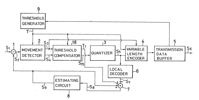
Referring now to FIGS. 1 ~ 3B, the prior art
technology of the present invention will be descri~ed.
The conventional image encoding/transmitting apparatus,
as shown in FIG. 1, includes a subtractor 1 for o~taining
a difference between an input signal Sl such as an image
signal and an estimation signal Sg and for outputting an
estimated error signal S2, a movement detecting circuit
2 for comparing a threshold value T with the estimated
error signal S2 to detect a movement or a change and for
generating and outputting a movement or change detect
signal S3 and a differential signal S4, a quantization
circuit 3 for quantizing the m~vement or change detect
signal S3 and the differential signal S4 to output a
quantizatLon signal S5, a variable length encoder 4 for
generating from the quantization signal S5 an encoded
signal S6 with a variable length and for outputting the
encoded signal S6, a transmissicn data buffer circuit 5
for temporarily storing the encoded signal S6 and for
: outputting the encoded signal 56 to the transmission side,
a local decoding circuit 6 for generating a reproduced
differential signal S7 from the quantization signal S5
deliveI~c from the quantization circuit 3 and outputting
the reproduced or regenerated differential signal S7, an
a~cer 7 fo- ach_e~-lng an addition on the reproduced
:
differential signal S7 and the estimation signal Sg and
for outputting a reproduced input signal S8, an estimating
circuit 8 for outputting an estimation signal S9 based on
- 8 -
12~20~9
the reproduced input signal 58' and a threshold
generating circuit 9 for monitoring the amount of the
encoded signal S6 accumulated in the transmission dat~
buffer circuit 5 and for generating an appropriate
threshold ~alue T.
The move~ent detecting circuit 2 comprises, as shown
in ~IG. 2, an absolute value circuit 10 for calculating
the absolute value ¦S2¦ of the estimated error signal S2,
a comparing circuit ll for effecting a comparison between
the absolute value ¦S2¦ of the estimated error signal S2
and the threshold value T and for outputting the movement
or change detect signal S3, and a zero allocator 12 for
allotting 0 and outputting 0 as the differential signal
S4 when the movement or change is not detected as a
lS result of the comparison in the comparing circuit 11.
The movement detect signal S3 is converted into a running
.
record R by use of the running length encode table 4a to
generate serial data. In addition, only when the movement
detect sIgnal 53 is indicating the validness/ the
quantization signal S5 is converted into a variable-length
record through the variable-length encode table 4b to
; senera~e serLal data~(FIGS. 23 ~ 2C). Reference numeral
4c indicates a multiplex operation control section.
In contrast to the configuration on the transmission
~ ~ ~ " ; : - ~
side of FIGS. 1 - 2B, the configuration on the reception
side is shown in FIGS. 3A - 3B. In FIG. 3A, the
equipment on the reception side includes a receivinq data
_ g _
292~i9
buffer circuit 13 for receiving and for temporarily
storing the encoded signal S6 delivered from the
transmission data buffer circuit 5 on the transmission
side, a variable length deooder 14 for decoding the
encoded signal S6 stored in the receiving data bu~fer 13
to output a reproduced guantization signal Sll, a local
decoding circuit 15 for outputting a reproduced
differential signal S12 based on the reproduced
quantization signal Sll, an adder circuit 16 for obtaining
the difference between the reproduced differential signaL
512 and the reproduced estimation signal Sl3 and for
reproducins the input signal Sl4 which corresponds to the
reproduced input signal S3 on the transmission side, and
an estimating circuit 17 for outputting the reproduced
lS estimation signal S13.
After the encoded signal 56 undergone the
multiplexing in the variable length encode circuit 4 i5 -
received by the receive buffer circuit 13, the data is
dist~i~uted to 'he -es~ect-ve decoce tables of variable
codes under control of the multiplex separation control
cirouit 14a. As a result of the decoding, the movement
detect signal anc: the quan;tlzation signal are attained.
Moreover, when the decoded movement detect signal
indicates the invalidness (= "0"), the quantization
. 25 signal is reset to `'0" by the flip-flop 14e, thereby
outputting the output Sll (FIG. 3B).
~ ~ :
- 1 0
:
Next, the operation on the transmission side ~will
'ae described with reference to FIGS. 1 - 2.
Assuming first the non-effective error in the
movement detecting circuit 2 to be d, the estimation
coefficient to be applied to the reproducad input signal
58 in the estimating circuit 8 to be A, and the dela~ of
the time t to be z t, the following relationships are
satisfied.
S2 = Sl - Sg
S4 = S2 + a
: ` S7 = S4 ~ Q
58 = 51 f S9 = 51 + Q + d
Sg = A. S8- z t
The subtractor 1 calculates the estimated error signal S2
representing the difference between the input signal S
and the estimated signal Sg, whereas the mavement
: detecting circuit 2 outputs the movement or change
: I ~ detection signal S3 and the differential signal S4 based
Gn the estimated er_or signal 52 calculated by the
subtractor 1.
A detailed description will be given of the operation
:of the move~ent ~et~ctins circuit 2 by referring to
:: : FIG.~2. The allotting absolut~ value circuLt 10 obtains
~: : the absolut2 value of the~estimated error signal S2 and
: ~ ~ 25 then the comparison circuit 11 achieves a comparison
: between the absolute value ¦S2¦ of the estimated error
signal 52 and the threshold value T generated by the
threshald value generating circuit ~.
-- 11 --
- ~Z92~S9
- The movement detection signal S3 is output in
conformity with the following conditions
S3 = 0 (invalid) lS21 T
S3 = 1 (valid) ¦S2¦ > T
When the movement or change is not detected, namel~, or
"S3 = 0", zero allocator 12 outputs "0" for the
differential signal S4.
On the other hand, the quantization circuit 3
converts the inputted differentlal signal S4 according to
an arbitrary characteristic. The variable encoding
circuit 4 receives the quantization signal S5 only when
the movement detection signal S3 is valid, namely, for
"53 = l" and, for example, conducts a run-length encoding
on the movement detection signal S3. For the quantizatlon
: 15 ~ signal S5, a code havinq a smaller code length is assigned
to a value in the neighborhood of "0" for which the
generation frequency is high and then the code is stored
: in the transmlssion data buffer circuit 5. ~he
: t-ansmission data bufLer circuit 5 outputs the
~ 20 accumulated datum as the~encoded signal S6 to a
:~ ~ ; transmission line. The threshold generating circuit 9
mon~ ors the ac~umulated amount of the transmission data
burfer circuit 5~and further controls the generation
amount of the encoded~data by generating an appropriate
~ : ,
~ 25 threshold value.
~, ~: : :
: Next, the operation on the reception side will be
described with reference to FIG. 3. The receiving data
12 -
:: ::
~zgz~
buffer circuit 13 first receives the encoded signal S~
undergone the variable length encoding on the
trans~ission signal and outputs the signal 56 to the
variable length decoder 14. Only when the movement
detection signal S3 undergone the decoding operation
indicates the validness, the variable length decoder 14
outputs the reproduced quantization signal Sll. If the
movement detection signal S3 indicates the invalidness,
the variable length decoder 14 outputs "0". Next, the
local decoding circuit 15 decodes the reproduced
quantization signal Sll and outputs the reproduced
differential signal 512 to the adder 16. The adder 16
adds the reproduced differential signal S12 to the
reproduced estimation signal S13 from the estimation
circuit 17 thereby to reproduce the input signal Sl4.
The operation to effect the data compression and
transmission by use of the differential signal is
referred to as the differential pulse code modulation
~to be abbrevlated as DPC.~ herebelow) system.
However, in the image encoding/transmitting apparatus
using;the DPC.~ system, the variable length encoding is
achieved on the dat~Im which is ]udged to be e~fective at
the~ste? of the variabl~ length encoding; consequently,
as the threshold value increases, the code having a short
code length to be assigned in the neighborhood of "0"
cannot be generated and hence the efficiency of the
encoding is deteriorated;~moreover, there has been a
- 13 -
problem that as the threshold value becomes greater, the precision
of the quantization is not improved for the quantization
characteristlc of the quantization circuit in the circuitr~ on the
transmission side even when the dynamic range of the effective datum
is narrowed.
SUMMARY OF THE INVENTION
In accordance with one aspect of the invention there is provided an
image encoding/transmitting method comprising: a preprocessing step
for effecting an analog-to-digital conversion on an image input
slgnal to generate a digital signal and for storing the digital
signal in a frame memory for each frame; an encoding processing step
for effecting a smoothing operation on the digital signal based on
an encoding control parameter such as a threshold value and for
encoding the smoothed digital signal; a transmission control
processing step for temporarily storing the encoded signal for each
: frame in a transmission data buffer and for sending the encoded
signal to a;transmission control unit; an encoding control parameter
control step for controlling the encoding control parameter based on
an amount of the encoded signals temporarily stored in the
transmission data buffer associated with a previous frame; and an
: auxiliary encoding control parameter controi step for extracting a
` portion of a current digital signal stored in the frame memory, for
effecting a pseudo encoding on the portion based on the encoding
control parameter calculated depending on the amount of the encoded
25 ~;slgnals:of the preceding frame, and for correcting the encoding
control parameter based on an amount of the pseudo encoded signals
having undergone the pseudo encoding, thereby causing the encoding
controI parameter to have an optimum value.
~: ; : - '
14
A description will be now given of the embodiments
suitable for the image encoding/transmitting apparatus
according to the present invention.
In FIG. 4A, reference numeral 18 indicates a
threshold compensation circuit for assigning a polarity
to the threshold value T output from the threshold
generating circuit 9 according to the differential
slgnal S4 supplied from the movement detecting circuit 2,
for generating the compensated differential signal S15 by
I0 effecting a subtraction between the threshold value Tl to
~which the polarity is assigned and the differential
: signal S4, and for outputting the compensated
differential signal S15.
- . ~s shown in FIG. 4B, the movement detect signal S3
1:5 is converted into a run length code R by use of the run
length encode table 4a to generate the serial dataO On
when t~e movement detect sisnal S3 is indicating the
vali~ness, the threshold value T and the quantization
; sLgnal ss are respectively converted into variable-length
:
:~
~ 15 -
'
~;~2(~59
records by use of the variable-length encode tabies
4b - 4c; thereafter, the records are con~erted into
serial data. The encode tables each are constituted
from a storage device such as an ROM. Reference numeral
4d indicates a multiplexing control section, In this
case, the multiplexing is accomplished as shown in
FIG. 4C.
In FIG. 5A, reference numeral l9 denotes a polarity
judgment circuit for judging the polarity of the
difference signal S4 and for outputting the polarity
signal Sl6, reference numeral 20 is a polarity adding
circuit for assigning the polarity to the threshold
value T output from the threshold generating circuit 9
according to the polarity signal S16, and reference
numeral 21 is a subtractor for achie~ing a subtraction
between the threshold value Tl with the polarity and the
differential signal S4 and for outputting the compensated
differential signal 515.~ The polarity judgment circuit
l9 lncludes a comparator l9a as shown in FIG. 5B.
~20 ~loreover, the subtractor 20 comprises a flip-flop 70a of
FIG. 5C. In FIG. 5B, the following condition is
~ satisfied.
- ~ if A < B (= ~io,.) then S 6 = "l"
else S = "0"
16
In FIG. 5C, the polarity signal S16 is used as the sign
~; bit of the threshold value T so as to be fetched by the
FF. This FF is reset to "0" when the movement detect
signaL S3 is indicating the invalidness (~ "0").
- 16 -
~2920~9
In FIG. 6A, reference numeral 22 denotes a
threshold compensation regeneration circuit for
generating the regenerated differential signal S21 from
the detection signal S17 output from the variable length
decoding circuit 14, the threshold value T, and the
regenerated, compensated difference signal S20 output
from the local decoding circuit 15 and for outputting
the regenerated differential signal S2l. The threshold
value regeneration circuit 14, as shown in FIG. 6B,
receives by means of the receive buffer circuit 13 the
encoded signal S6 undergone the multiplexing in the
:: variable-length encode circuit 4 on the transmission
side, distributes the data to the respective decode
tables of the variable-length code under control of the
multiplexing separation control circuit, and obtains as
the results of the variable-length decoding operation the
movement detect signal S17, the threshold value T, and
the quantization signal Slg. When the move~ent detect
signal indicates the invalidness, the threshold value T
and the quantization signal Slg are not delivered.
Incidentally, the decode tables each are constituted from
: a memory device such as an ROM.:
: In addition, in FIG. 7A, reference numeral 23 is a
:: polarity judgment circuit for judging the polarity of the
: ~ 25~ : regenerated, compensated differential signal S20 and for
;~ outputting the polarity signal S23, reference numeral 24
.:
~: designates a polarity adding circuit for assigning the
~ .'
~ - 17 -
12~
polarity to the threshold value T according to the
polarity signal S23 and for outputting the.threshold
value Tl with the polarity, and reference numeral 25
indicates an adder for outputting the regenerated
differential signal S21 by adding the threshold value T
with the polarity and the regenerated, compensated
differential signal S20.
Next, the operation on the transmission side of the
present invention will be described with reference to
: 10 FIGS. 4A - 5C.
First, assuming the non-effective error in the
movement detecting circuit 2 to be d, the estimation
coefficient to be applied to the regenerated input signal
S8 in the estimating circuit 8 to be A, and the delay of
L5 the time t to be z t, the following relationships are
.
satisfied.
S2 Sl Sg
54 S2 + -
515 = 54 ~ T
20~S7 = S7 + Q
: : :56 = S9 + S7 + T = Sl + Q ~ d
: -t
: Sg = A- S8- Z
: : The subtractor 1 here calculates the estimated error
slgnal S2 representing the dlfference between the input
25~ signal Sl and the estimated signal~Sg, whereas the
movement detecting circuit~2 outputs the movement
detection signal S3 and the differential signal S4 based
:
~ - 18 -
::
~2~
on the estimated error signal S2 calculated by the
subtractor 1.
The operation of the movement detecting circuit 18
in this case is the same as that of the conventional
system.
On the other hand, the threshold compensation
circuit 18 outputs the threshold value Tl with the
polarity and the compensated differential signal 515
based on the movement detection signal S3 and the
differential signal S4.
The operation of the threshold compensation circuit
18 in this case will be described in details with
re~erence to FIG. 5.
In FIG. 5A, the polarity judgment circuit 19 judges
the polarity of the differential signal S4 and outputs
the polarity signal S16 to the polarity adding circuit
20. On receiving the polarity signal Sl6, the polarity
adding circuit 20 assigns the polarity to the threshold
value T from the threshold gene~rating circuit 9 and
outputs the resultant signal as the threshold value T
~ ~ with the polarity. However, in the case where the
;~ ~ movement detection signal S3 indicates the invalidness,
the threshold value Tl with the polarity is set to 0.
In this case, there exists also a method in which the O
~ is judged in the polarity judgment circuit 19 and the
:
polarity adding~circuit 20 sets the threshold value S
with the polarity to 0 according to the judgment. By
-- 19 --
,
1~2~g
subtracting the threshold value Sl with the polarit~
from the differential signal S4 in the subtractor 21,
the threshold value is compensated and hence the
compensated differential signal S15 is outputted. The
compensated differential signal S15 is converted into
the quantization signal S5 in the quantization circuit 3
and is delivered to the variable length encoding circuit
4 and the local decoding circuit 6. When the movement
detection signal S3 is valid, the variable encoding
circuit 4 receives the quantization signal S5 and the
threshold value T, and for example, effects a run length
encoding on the movement detection signal S3. For the
quantization signal S5, the variable length encoding
clrcuit 4 assigns a code with a short code length to a
value in the vicinity of 0 for which the generation
: frequency is high and accumulates the code in the
transmission data buffer circuit 5; thereby outputting
the signal as the encoded signal S6 to the transmission
line. Moreover, in the threshold generating circuit 9,
the accumulated amount of data in the transmission data
buffer 5 is monitored so as to generate an appropriate
threshold value T to control the generation a~ount of the
~ encoded datum. On the other hand, the local decoding
: : circuit 6 decodes the quantization signal S5 into the
::
: 2S : regenerated, compensated differential signal S7, which is
: ~:
; then fed to the adder 7. The- adder 7 ~dds the threshold
~: value~T, the estimated signal S8, and the regenerated,
- 20 -
.
~292059
compensated differential signal S7 to obtain the
regenerated input signal S8. The estimating circuit
delays the regenerated input signal S8 by a period of
time t beforehand set, multiplies the signal by the
coefficient A, and outputs the resultant signal as the
estimated signal Sg. If the time t is set to the period
of time of a frame when the input signal Sl is an image
signal, a frame-to-frame DPCM transmitting apparatus is
implemented; whereas, if the time t is set to the period
of time of a field, a field-to-field DPCM transmitting
:: apparatus is materialized.
In addition, in the embodiment above, the same
effect can be attained by reducing the threshold value
for the transmisslon by means of a control in which the
:15: generation and update of the threshold value are
conducted at an interval of an arbitrary period of time
: T
Next, the operation on the reception side will be
: ~ described with:reference to FIGS. 6A - 6B. The encoded
,
signal S6 undergone the variable length encoding on the
~ : ~ :transmission side is received b~ the receiving data
:: ~ buffer circuit 13. Only when the decoded movement
,
;detectlon signal S1~7 is~valid, the variable length
: decoding circuit 14 outputs the threshold value T and
: 25~ the~regenerated quantization signal Slg. When the signal
S17 is invalid, 0~is outputted. The local decoding
cLrcuit 15 decodes the regenerated quantization signal
- 21 -
9Z~
Slg into the regenerated, compensated differential
signal; furthermore, the regenerated diCferential signal
S21 is regenerated in the threshold compensation
regeneration circuit 22. The opération will be described
with reference to FIG. 7A. The polarity of the
regenerated, compensated differential signal S20 is
judged by the polarit~ judgment circuit 23, the polarity
is assigned to the threshold value T depending on the
polarlty signal S23 representing the positive or negative
polarity, and the resultant signal is delivered as the
threshold value Tl with the polarity. However, when the
movement detection signal S17 indicates the invalidness,
; the threshold value Tl with the polarity is set to O.
Moreover, the adder 25 adds the regenerated, compensated
differential signal~S20 to the threshold value Tl with
the polarity, thereby attaining the regenerated
differential signal S21. The adder 16 adds the esti~ated
signal S22 from the estimating circuit 17 to the
regenerated differential signal S21 so as to regenerate
the~ objective input signal Sl on the transmission side.
The operation of the threshold compensation ~ircuit
can be~represented by numeric values as shown in FIG. 7B.
This~example shows~a c~ase of T = 5. FIG. 7C is an
input/output characteristic graph corresponding thereto.
The broken lines indicate the conventional example,
whereas the solid lines represent the characteristic of
the present invention.
- 22 -
~ ~ .,
lZ~Z~S9
As described above, even if the invalid data period
(-T-O-T) occurs due to the movement detect circuit, the
invalid data period can be canceled by effecting the
threshold value compensation according to the present
invention, which enables to increase the quantization
precision as compared with the conventional apparatus.
As described above, according to the embodiment of
the present invention, the polarity of the differential
signal is judged, a polarity is assigned to the threshold
value depending on the judgment, the compensation of the
differential signal is achieved according to the
; threshold value to which the polarity is assigned, and
the compensated differential signal undergone the
quantization is used for the transmission and reception;
consequently, the generation of the code with a short
code length allocated in the neighborhood of 0 is
suppressed and hence the efEiciency of the communication
is improved.
Next, the second embodiment of the present invention
will be described.
The datum compressing/transmitting apparatus
utilizing the differential pulse modulation system
~according to the second embodiment includes a transmis-
:
sion circuit section for effecting the data compression
25; ~and transmission on the digitaI input signal by use of
the differential pulse modulation and a reception circuit
section associated with the transmission circuit section.
~: :
- 23 -
~2920~9
.
FIG. 8A shows the bloc~ construction diagram of the
transmission circuit section of the embodiment
In the second embodiment, the quantization circuit
comprises an adaptive quantization circuit 3 having a
plurality of quantiZation characteristics. The adaptive
quantization circuit 3 selects a characteristic depending
on the threshold value T, conducts an adaptive
quantization on the differential signal S4, and outputs
the adapted quantiZation signal S5.
The adaptive local decoding circuit 6 is disposed
corresponding to the adaptive quantization circuit 6,
decodes the adapted quantization signal 55, and outputs
the regenerated differential signal S7. Incidentally,
the same reference numerals are assigned to the same
lS components as those of the prior art example and the
description thereo will be omitted.
FIG. 9A is a block diagram for explaining the
adaptive quantization circuit 3 in details. The character
selecting circuit 28 selects a quantization character-
istic depending on the threshold value T and thenquantizes the di~ferential signal S4.
FIG. 3B is a block diagram for explaining the
~; adaptation local decoding circuit 6 in details. The
character selecting circuit 29 selects a decoding
characteristic depending on the threshold value T and
then decodes the quantization signal S5; furthermore,
the obtained signal passes the zero allocation circuit
- 24 -
lZ~2~5~
25 so as to be subjected to the zero allocation
depending on the movement detection signal S3
Next, the flow of the signal will be described. As
shown in FIG. 8A, assuming the digitalized input signal
such as an image signal to be Sl, the estimated signal
calculated by the estimating circuit 8 (to be described
later) to be Sg, the estimation error signal to be S2,
the differential signal to be S4, the regenerated
differential signal to be S7, and the regenerated input
signal to be S8, these exists the following relationships
among the respective signal values.
S2 = Sl - 59
S4 = S2 + d
S7 = S4 + Q
S8 = Sg + S7 = Sl + Q
Sg = A- S8- z t
where, d is the non-effective error in the movement
detection circuit, Q stands for the quantization error,
A indicates the estimation coef~icient, and z t denotes
a delay of the time t.
The estimating circuit a delays the regenerated
input signal S8 by a period of time t beforehand set,
multiplies the obtained signal by the coefficient A, and
outputs the estimation signal S9.
Like FIG. 2, in the movement detecting circuit 2,
.
assuming the absolute value of the estimated error signal
S2 calculated by the absolute value circuit lO to be ¦S2¦
- 25 -
~2~2~5~
and the threshold value to be T, the value of the
movement detection signal V calculated by-the comparing
circuit 11 is determined as follows.
If ¦S2¦ ~ T, then V = 0 ~invalid)
else V = 1 (valid).
Furthermore, if the predetermined amount of movement
is not detected (within the invalid data range), the zero
allocation circuit 12 allocates "0" to the estimated
error signal 52 and hence the differential signal S4 is
outputted as "0" to the adaptive quantization circuit 3.
As shown in FIÇ. 9A, the differential signal S4
inputted to the adaptive quantization circuit 3 is
converted into the quantization signal S5 according to
the quantization characteristic specified by the
~15 character selecting clrcuit 29 which changes over the
characteristic depending on the threshold value T and the
:
` quantization signal S5 is then outputted to the variable
length encoding circuit 4.
A description will be here given of the quantization
~20 characteristic example in reference to FIG. ll(a).
:
The dot-and-dash line indicates a characteristic
example in th case of T = 0~, whereas the solid line
,
denotes~a characteristic example in the case of T = 3.
; As~shown in this diagram, when the datum of the
~ differential signaI 54 i~s in the invalid data range
T < data < +T), the~ quantization is not accomplished,
namaly, the quantization is effected only for the datum
- 26 -
~ . .
:~ :
, .
~2059
in the valid data range (data < -T or +T ~ data). As
can be seen from FIG. 9A, the quantization characteristic
selected by the character selecting circuit 28 is such
that the quantization output on the differential signal
within the invalid data range (within the specified
range of the correspondiny threshold value) becomes to
be "0", which improves the quanttzation accuracy.
The characteristic selecting circuit 28, as shown
in detail in FIG. 9C, comprises a flip-flop 28a (FF) to
which the decoded quantization signal selected by the
characteristic selecting circuit 28 is delivered as an
input signal and is reset to "0" when the movement detect
signal VD indicates the invalidness (V = 0).
The variable length encoding circuit 4 receives
only the quantization signal S5 for which the movement
detection signal S3 is valid (V = l~ and effects the run
length encoding on the movement detection signal S3.
For the quantization signal S5, a code with a short code
length is assigned to the value in thse neighborhood of 0
for which the generation frequency is high, and the
resul~tant code is transmitted to the transmission data
buffer circuit S. The data accumulated in the
transmission data buffer circuit 5 is sent as the encoded
signal S6 to the transmission path.
In addition, as shown in FIG. 8A, the quantization
~signal S5 is also delivered to the adaptation
quantization circuit 6.
- 27 -
:
Moreover, as shown in FIG. 8B, the threshold value
generator circuit 9 includes a conversion table 9a used
to convert an input data into a threshold value based on
the accumulated amount of the data. FIG. 8C shows the
relationships between the accumulated data amount and the
threshold value.
On the other hand, as shown in FIG. 98, the adaptive
decoding circuit 6 selects a decoding characteristic by
means of the character selecting circuit 29 corresponding
to the quantization characteristic selected by the
adaptation quantization circuit 3. As shown here in
FIG. 9D, the characteristic selectlng circuit comprises a
memory device such as an RO~I and the selection signal
thereof is determining by use of the mapping in which the
threshold value T is used as an address input. Moreover,
the allocation zero circuit 25 allocates the invalid
datum "0", which is then delivered as the regenerated
differential signal 57. FIG. llB shows a decoding
characteristic e~ample. In the adder 7, the regenerated
differential signal S7 is added to the estimation signal
Sg to obtain the regenerated~input signal S8 to the
supplied to the estlmating circuit 8.
The threshold generating circuit 9 monitors the data
accumulation amount of the transmission data buffer
circuit 5, generates an appropriate threshold value
according to the data accumulation amount, and thereby
achieves a smoothing operation on the data code amount.
~,:
- 28 -
~2~59
FIG. 10 is the block construction diagram
illustrating the reception circuit section of the data
compressing/transmitting apparatus utilizing the
differential pulse modulation system according to the
present invention. The reception data buffer circuit 13
temporarily stores the encoded signal S6, the variable
length decoding circuit 14 decodes the encoded signal
S6, the adaptive local decoding circuit 15 outputs the
regenerated differential signal S12, and the estimating
circuit 17 estimates the regenerated signal Sl.
Here, the detailed constitution of the adaptive
local decoder circuit 15 is the same as that of the
: circuit 6 of FIG. 8A. In addition, the quantization
characteristic and the decoding characteristic
associated with the memory device such as an ROM are the
: same as those shown in FIGS. 9A - 9D.
The regenerated signal Sl is calculated by the adder
16 from the estimated signal 513 and the regenerated
differential signal S12.
Next, the flow of the signal in the reception
circuit section will be described. The encoded signal S6
.
sub~ected to the variable length encoding in the
transmission circuit section is received by the receiving
data buffer circuit 13 and is then transmitted to the
: 25~ variable length decoding circuit 14.
Only when the movement detection signal Sllc decoded
in the variable length decoding circuit 14 indicates the
- 29 -
~29Z~S9
valid data range (V = 1), the quantization signal Slla
and the threshold value Sllb are fed to the local
decoding circuit 15. When the decoded movement detection
signal S3 indicates the invalid data range (V = 0), "0"
is delivered to the local decoding circuit 15.
Moreover, like the adaptive local decoding circuit
~ of the transmission circuit section, the adaptive
local decoding circuit 15 selects a decoding
characteristic depending on the threshold value Sllb.
The quantization signal Slla is then decoded into the
regenerated differential signal S12 and is added by
means of the adder to the estimated signal S13 from the
estimating circuit 17, thereby the encoded signal S6
from the transmission circuit section is regenerated as
a signal S14.
In this embodiment, the same effect can be attained
by reducing the threshold value for the transmission
through an operation to generate (update) the threshold
value at an interval of an arbitrary period of time T
(e.g. a frame period).
Prior to the description of the third embodiment of
the present invention, description will be given of the
technology adopted as the basis of the third embodiment
and OL the outline thereof.
The third embodiment relates to a vector quanti~er
for encoding image signals with a high efficiency, and
in particular, to a miniturized vector quantizer.
- 30 -
-- ~.292~1S9
FIG. 12 shows the technology as the basis of the third
embodiment. This diagram illustrates a block diagram o~
the n-th stage of the vector quantizer. As shown in
FIG. 13, the vector quantizer includes a multi-stage
connection of a plurality of stages.
In FIG. 12, reference numeral 31 is a vector output
circuit, reference numeral 32 indicates an input index,
reference numerals 33a - 33b are distortion operating
circuits, reference numeral 34 designates an input
L0 vector, reference numeral 35 indicates a comparator,
reference numerals 36a - 36b denote distortions,
reference numeral 37 is an index output circuit,
reference numeral 38 indicates a delay circuit, reference
numeral 39 stands for an output vector, reference numeral
310 denotes an output index, and reference numeral 311
designates a quantizer output index. The encoding
section 320 comprises the respective circuits above.
~; Incidentally, reference numeral 321 in this diagram
indicates the encoder at the final stage.
Next, the operation of this configuration will be
described. When the input index 32 is received, the
: -
vector output circuits~31a - 31b select output vectors
from a~group of output vectors beforehand prepared (code
;book) corresponding to the~input;index and then deliver
the output vectors. The respective output vectors are
supplied to the distortion computation circuits 33a -
33b, which calculate the distortions (distances) with
,
- 3l -
:
respect to the input vector sent from the input buffer
312. The distortions 36a - 36b outputted as a result of
the computation fro~ the respective distortion
computation circuits 33a - 33b are fed to the comparator
35, which effects a comparison therebetween. For the
distortion 36a < the distortion 36b, "0" is output;
whereas for the distortion 36a > the distortion 36b, "1"
is output. Next, the distortion compare value is output
together with the index 32 from the index output circuit
37 to the encoding section 320 of the next stage so as to
be used to generate a new input index. The input vector
34 to be subjected to the distortion computation at the
next stage is sent via the delay circuit 38 to the
encoding section 320 of the subsequent stage, so that
the distortion is computated with respect to the output
veotor selected and output by use of the new input index.
The distortion computation is continuously repeated up to
the encoding section 321 of the final stage so as to
minimize the total of the distortion through a conversion,
thereby generating the final quantizer output index 311.
In FIG. 13, the input vector and the input index to
each encoding section 320 are respectively the output
vector 39 and the output index 310 from an encoding
section 320 of the previous stage. For the encoding
s~ection 321 at the final stage (the 10-th stage in this
case), since there does not exist the encoding section
320 of the succeeding stage as compared with the encoding
32 -
-
~lX~;~059
sections 320 of from the first to the ninth stages, the
delay circuit 38 is not required. The output index Crom
the final stage is delivered as the quantizer output
index 311.
As shown in FIGS. 12 - 13, the prior art vector
quantizer is configured such that the input vector (input
datum) and the input index for selecting an output vector
are sequentially transmitted -to the next encoding section
320 while updating the input index in each encoding
section 320 so as to generate the quantizer output index
in the final encoding sectlon 321, which consequently
leads to problems that the size of the circuitry is
increased and that the idle time or the wait time occurs
in the encoding sections and hence the overall circuitry
cannot be effectively utilized.
According to the vector quantizer of the embodiment,
there is provided a quantization index output circuit in
which the input image signal is subsampled in the
quantization pre?rocessing circuit to thin out pixels,
the respective pixel signals are used to form an
n-dimensional input vector, and each input vector is
: stored in the input buffer corresponding to each pixel
signal; furthermore, the input vector is supplied to the
ncoding section corresponding to the input buffer at an
~:25 interval of the processing period. The encoding section
: calculates the distortion between the input vector and
: the output vector updated at an interval of the processing
33 -
.
period. Based on the distortion, the input index
generating means generates a new input index for
selecting the output vector, and based on the input
index, the quantizer output index is generated and is
output from a quantization index output circult.
Next, the third embodiment of the present invention
will be described with reference to the drawings.
FIG. 14A is a schematic block diagram depicting the
entire configuration of the third embodiment in which
reference numeral 316 denotes an input image, reference
numeral 317 is an quantization preprocessing circuit,
reference numerals 311a - 31b designate vector output
circuits for outputting vectors corresponding to the
input index 32, reference numerals 33a - 33b indicate
~15 distortion computation circuits for respectively
calculating the distortion between~the input vector 34
and the vectors delivered from the vector output circuits
31a - 31b, reference numeral 35 denotes a comparator,
reference numeral 36a stands for a distortion outputted
from a circuit equivalent to the distortion computation
circuit 33a in the encoding section 313a and the
distortion computation circuit 33a in the respective
encoding~sections 313b, 313c, and 313d, reference
numeral 36b designates a distortion outputted from a
circuit;equivalent to the~distortion computation circuit
33b in the encoding section 313a and the distortion
computation circuit 33b in the respective encoding
.
~ ~ ~ - 34 -
1~9ZOS9
sections 313b, 313c, and 313d, reference numeral 37
indicates an index output circuit, reference numeral 311
represents a quantizer output index of the vector
quantizer, reference numerals 312a, 312b, 312c, and 312d
are input buffers for storing the blocks A, B, . , H
obtained by dividing the input vector 34 as shown in
FIG. 15, reference numerals 313a, 313b, 313c, and 313d
denote encoding sections, reference numerals 314a, 314b,
314c, and 314d indicate history circuits for outputting
10 indices for the blocks of A, B, , H, and reference
numeral 315 denotes a quantization index output circuit
for outputting the index of the vector ~uantizer circuit
associated with the input vector. As shown in FIG. 14B,
the history circuits 314a - 314d each comprise a first
flip-flop circuit 601 for receiving an output from the
output index circuit 37, a second flip-flop circuit 602
for the same purpose, an output control circuit 603, a
third flip-flop circuit 604 for receiving the respective
outputs from the first and second flip-flop circuits
601 - 602, and a pattern comparing circuit 605 for
delivering a history signal to the encoder 313a based on
the output from the third flip-flop circuit 604. The
pattern ccmparing circuit 605 is constituted, for example,
from a code book. FIG. 15 shows a block attained by
dividing the image of the third embodiment in which A - H
indicate subblocks. The input buffers 312a - 312d
respectively store subblocks A - B, C - D, E - F, and
:
- 35 -
~.Z9~
G - H. The embodiment has been described ~ith reference
to a vector quantizer including ten stages. FIGS.
16(a) - 16(g) show the indices and quantizer output
index 311 to be output from the index output circuit 37
at each stage. ~
Next, the operation of the embodiment will be
described. The image 316 supplied to the system is
thinned out in the quantization preprocessing circuit
317. (Refer to FIG. 17 for details.) Before the input
vector 34 is supplied to the vector quantizer, the
blocks A - B, C - D, E - F, and G - H of FIG. 15 are
respectively written in the buffers 312a - 312d.
Thereafter, the image data is read as blocks of A - B,
C - D, E - F, and G - H in parallel from the associated
buffers 312a - 312d, respectively, and the vector
quantization is accomplished by executing the read
operation ten times for each block. (Refer to ~IG. 1~3
for details.) However, prior to the operation above,
the vectors read from the ~uffers 312a, 312b, 312c, and
312d are respectively supplled to the distortion
computation circuits 33a and 33b. The buffers 312a -
312d are added to effect a concurrent processing by
separating the input serial data into four data groups.
The details of these buffers 312a - 312d are shown in
FIG. 17C.
Furthermore, the vectors output from the vector
output circuits 31a - 31b according to the input index
12~
32 are also delivered to the distortion computation
circuits 33a - 33b. The distortion computation circuits
33a - 33b calculate the distortions between the vectors
input from the input buffers 312a - 312d and the vectsrs
output from the vector output circuits 31a - 31b,
respectively. In this operation, to prevent the
distortions from being delivered from the encoding
sections 313a - 313d to the comparator 35 at the same
time, the distortions are output therefrom in the
sequence of encoding sections as 313a, 313b, 313c, and
313d. Next, the distortions are input to the comparator
35 and "0" is output from the comparator if the
distortion 36a is less than the distortion 36b;
otherwise, "1" is output. Based on the output from the
lS comparator 35 and the index previously supplied, the
index circuit 37 outputs a new index. From the history
circuits 314a - 314d, the indices of the vectors of the
respective blocks A - B, C - D, E - F, and G - H are
output to the vector output circuit for the next
distortion computation. In additiont the indices are
also output to the index output circuit 37 to attain the
next new index. This operation is repetitiously executed
~rom the firs~ stage to the tenth stage/ and the index
delivered from the last operation at the tenth stage is
output as the vector quantizer index from the
; quantization index output circuit 315. The output
waveforms at the respective sections descri~ed in
- 37 -
~29Z~59
conjunction with FIG. 14B of the history circuits
314a - 314d are as shown in FIG. 18.
As described above, according to the third
embodiment, the input image is subsampled, the pixels
are subjected to the thinning-out operation, and the
n-dimensional input vector to be shaped is minimized.
Thereafter, for the input vectors of the same image, the
distortion operation is repetitiously executed by the
same distortion operation circuit to converge the total
of the distortions, thereby minimizing the resultant
value of the total. For other vectors, the distortions
are concurrently calculated by the respective distortion
operation circuits, and based on the distortions, the
quantizer index is generated for each pixel signal;
I5 consequently, the size of the circuitry can be
miniaturized and the entire circuitry can be efficiently
operated without idle operations.
Prior to the description of the fourth embodiment of
,. .
the present in~ention, description will be given of the
technology adopted as the basis of the third embodiment.
FIG. 19 shows an image encoding/transmitting
apparatus to which the frame-to-frame encoding method
utllizing the vectorizing method, namely, the image
encoding/transmitting method as the basis of the fourth
25~ embodiment incIuding the movement compensation is applied.
As shown in this diagram, the image encoding/
; transmitting apparatus primarily includes a preprocessing
::
- 38 -
~.2~2W9
section 41, a movement compensation section 42, and a
vector quantization section 43.
The preprocessing section 41 generates from the
image input signal 400 blocks each containing k pixels
S existing in the neighborhood of each other in the image
to form a k-dimensional vector signal 401 for each block,
whereas the frame memory 44 is provided to store the
image signal formed in a block in advance in time by a
frame of the current image signal.
The movement compensation section 42 includes a
reference block generating section 42a for generating as
a reference blocks a plurality of blocks each including
the current vector signal 401, a block corresponding to
the current vector signal 401, and a block stored in the
frame memory corresponding to the same position in the
image and for calculating the block position information
402al and the vector signal 402a~ and a distortion
computation section 42b for calculating the distortion
~for e.Yample, the Euclid distortion, the absolute
distortion, etc.) between the current vector signal 401
and the reference vector signal 402a2 and for selecting
a block having the minimum distortion from the reference
blocks.
The subtractor 45 achieves a subtraction between the
; 25 current vector signal 401 and the vector signal 402b2 of
the block selected by the movement compensation section
- 39 -
~Z92~59
42 and sends the differential vector signal 405 to the
vector quantizing/encoding section 43.
The vector quantizing/encoding section 43 comprises
an arithmetic section 43a for computing the average
value m and the variance a from the differential vector
signal 405, a validness/invalidness judgment circuit 43b
for judging the validness or invalidness of the selected
block based on the average value m, the variance a, and
the threshold values Tl and T2 controlling the
compression amount of the information volume, a
normalizing section 43c for normalizing the differential
: vector signal 405, a code block 43d for storing patterns
of a plurality of the normalized image vector signals,
: ~ and a vector quantizing section 43e for selecting a
: 15 pattern from the code book 43c which is the same as or
similar to the normalized differential vector signal 403c
: normalized by the normalizing section 43c and for
~ ~ encoding the selected pattern number, the average m, and
: : the variance a.
~: 20~ ~ ~ Ne~t, the flow of the signal will be described.
: : First, the image input signal 400 is subjected to
the block generation in the preprocessing section 41 and
: is ~thereby converted into the vector signal 401.
Ther2after, the reference blocks are generated in
:
25~- the movement compensation section. From the reference
bIoc~s,~a block having the smallest distortion with
respect~to the vector signal:401 is selected, and then
- 40 -
- ~X~Z~S9
the selection ~lock position information 402bl and the
selection vector signal 402b2 are supplied to the
subtractor 45.
In the subtractor 45, a subtraction is then
accomplished between the vector signal 40l and the
selection vector signal 402b2, and the differential vector
signal 405 is delivered to the vector quantizing/encoding
section 43.
In the vector quantizing/encoding section 43, the
differential vector signal 405 is processed by the
arithmetic section 43a to calculate the average value m
and the variance a of the differential vector signal 405.
Thereafter, the validness/invalidness judgment circuit
43b judges the validness or invalidness as represented
by the following expressions by use of the threshold
value Tl for the average value and the threshold value
T2 for the variance.
: ~ m < Tl and a < T2: Invalid
~ m _ Tl or a > T2: Valid
: ~ 20 If the judgment results in the invalidness, the
: current block is assumed to be identical with the
: selected block and hence only the selection block
position information 402bl is encoded and the resultant
signal is temporarily stored in the transmission data
::
~ 2S buffer 46.
:: :
: : ~ On the other hand, if the judgment results in the
validness, the differential vector signal 405 is
:
- 41 -
~ 2~Z~59
normalized as the datum to be transmitted in the
normalizing section 43c according to the following
formula.
Yi (Xi ~ m)/a
(where, i = 1, 2, .. , k)
yi: i-th element of the normalized vector
xi: i-th element of the differential vector
Thereafter, the normalized differential vector
: signal 403c is quantized and encoded in the vector
~ quantizing section 43e as follows.
First, a pattern which is most similar to the
; normallzed differential vector signal 403c is selected
: : from the code book 43d. As the transmission information,
the pattern number, the selection position information
lS 402bl, the average value m, and the variance a are
encoded and the resultant signals are temporarily stored
in the transmission data buffer 46.
The image encoded signals temporarily stored in the
transmission data buffer 46 are transmitted in the
frame-by-frame fashion.
On the other hand, the threshold values Tl - T2 are
controlled accordinq to the amount of the image encoded
signals stored in the transmission data buffer 46
: asso~iated with the previous frame such that the threshold
valuas are set to great values for the great amount of
: the signals and are set to small values for the small
~.
- 42 -
~2~ 059
amount of the signals, thereby controlling the degree of
the compression for each frame.
According to the image encoding/transmitting
apparatus shown in FIG. 19 as described above, as a
result of the movement compensation processing step,
when the differential data between the input block and
the selected block is within the threshold value range
in the encoding processing step, the selected block is
directly reproduced as an image.
In this operation, if the selected block or the
input block has a strong contour line even whén the
differentlal datum is within the threshold value range,
there has been a problem that the contour line is
shifted in the image as shown in FIG. 21. This
phenomenon is emphasized in a case where the distance
between the input block and the selected block is great.
Such a problem takes place because the mismatching in the
movement compensation cannot be fully compensated.
Next, the fourtn embodiment implemented to solve
the problem above will be concretely described.
FIG. 20A is a block configuration diagram showing
the image encoding/transmitting apparatus to which the
fourth embodiment is applied. In FIG. 20A, the same
reference numerals are assigned to the same components
as those of FIG. 19 and the description thereof will be
omitted.
- 43 -
~292059
The characteristic item of the embodiment is a
threshold control section 47 which includes a threshold
generating circuit 47a controlled by the amount of th~
encoded signals temporarily stored in the transmission
data buffer 46 for effecting a threshold control such
that the threshold value is increased when the amount of
the encoded signals ic. great and the threshold value is
decreased when the amount of the encoded signals is small
and a distance calculating circuit 47b for calculating
the distance between the current input block and the
selection block selected by the movement compensation
section 42. The threshold generating circuit 47a
includes, as shown in FIG. 20B, a threshold generating
section 471 and an auxiliary threshold control circuit
472 for decreasing the threshold values based on the
calculated distance when the distance is great.
Next, the flow of the signal will be described.
The image input signal 400 is first subjected to the
block generation in the preproc ssing section 41 so as to
be converted into the vector signal 401.
In the movement compensation section 42, reference
blocks are generated and a block having the smallest
distortion with~respect to the vector signal 401 is
- ~ selected from the reference blocks. Theréafter, the
selection block position information 402bl and the
selection vector signal 402b2 are supplied to the
subtractor 45, while the selection block position
:
- 44 -
:
~2~Z~59
information 402bl is sent to the distance calculating
section 47b of the threshold control section 47
The details of the operation will be described .Jith
reference to FIGS. 20C - 20D. FIG. 20C is a schematic
diagram showing positions of pixels of a reference block,
namely, pixels exist as indicated by small circles (o),
1 - 13 . From the distortion operation section 42b
sends to the distance calculating section 47b the number
(one of the numbers 1 - 13 in this case) of the block
having the smallest distortion among the reference
blocks. The distance calculating section 47b converts
the number into a distance by use of a map data
beforehand set as shown in FIG. 20D and then transmits
the distance to the threshold generator circuit 47a.
The threshold values Tl - T2 are controlled
- according to the amount of the image encoded signals
stored in the transmission data buffer 46 associated with
the previous frame such that the threshold values are set
to great values for a large amount of the signals and are
set to small values for a small amount of the signals;
however, when the distance of the output 407b from the
distance calculating circuit 47b exceeds a fixed value,
~the auxiliary control is conducted to reduce the
threshold values.
The subtractor 45 effects a subtraction between the
vector signal 401 and the selection vector signal 402b2,
and then the differential vector signal 405 is delivered
to the vector quantizing/encoding section 43.
- 45 -
~;29~5~
Thereafter, in the vector quantizing/encoding
section 43, the differential vector signal 405 is
processed in the arithmetic section 43a to calculate the
average value m and the variance a of the differential
vector signal 405. In the validness/invalidness judgment
circuit 43b, the validness or invalidness is judged by
use of the threshold value Tl for the average and the
threshold value T2 for the variance according to the
following expressions.
m < Tl and a < T2: Invalid
m _ Tl or a _ T2: Valid
In this operation, if there exists a great distance
between the current block and the selected block, the
control is effected to reduce the threshold values by the
threshold control section 47 as described above;
consequently, when the distance between the current block
and the selected block is large, the possibility of the
invalidness is lowered.
I~ the judgmen~ resul's in the invalidness, the
current block is assumed to be identical with the
selected block and only the selection block position
information 402bl is encoded and the resultant signal is
temporarily stored in the transmission data buffer 46.
~ On the other hand, if the judgment results in the
validness, the differential vector signal 405 is
normalized as the datum to be transmitted in the
normalizing section 43c according to the following formula.
- 46 -
~L292~59~
Yi (Xi ~ m)/a
(where, i = 1, 2, ..., k)
y~ th element of the normalized vector
. lxi: i-th element of the differential vector
Thereafter, the normalized differential vector
signal 403c is quantized and encoded in the vector
quantizing section 43e as follows.
First, a pattern most similar to the normalized
; differential vector signal 403c is selectéd from the code
book 43d. As the transmission information, the pattern
. : : number, the selection position information 402bl, the
:average ~alue m, and the variance G are encoded and the
resultant signals are temporarily stored in the
: : ~ transmission data buffer 46.
~ The image encoded signals temporarily stored in the
transmission data buffer 46 are transmitted in the
frame-by-frame fashion :
~: . According to the embodiment, for a selected block
with a great distance for which the possibility of the
20~ mLsmatching is high as a result of the movement
compensation, the control is effected to lower the
threshold values and to conduct the encoding and
: transmission of the differential vector signal between
the: lnput block signal and the selected block signal,
~ wh~ich leads~ to an effect that the occurrence of the shift
;of the~ contour of the block is minimized.
47 -
,: :
~ .
~ ~2059
In addition, according to the embodiment, although
a description has been given of an example of the
auxiliary threshold control in which the threshold val~1es
are set to the lower values as the distance between the
S distance selection block and the input block is increased,
the same effect can be attained by conducting a step~lise
control in which several kinds of threshold values are
provided depending on the distances.
Next, the fifth embodiment of the image encoding/
transmitting apparatus will be described according to the
present invention.
First, prior to the description of the concrete
contents of the fifth embodiment, the general example of
the technology adopted as the basis of the fifth
lS ~embodiment will be described.
FIG. 22 shows the image encoding/transmitting
apparatus as the basis of the fifth embodiment.
In the analog/digital converting section (to be
referred to as an A/D converting section) 51 of FIG. 22,
the pixels obtained by effecting the analog/digital
conversion on the image input signals are processed to
- generate groups each containing k pixels being in the
neighborhood of each other in the image, so that for each
block, a k-dimensional vector input signal is generated.
A frame of vector signals are then stored in the frame
memory 52, thereafter the vector signals are transmitted
to the encoding section 53 in the block-by-block fashion.
- 48 -
::
12~2,~9
Incidentally, the encoding section 53 is provided
- with a previous frame memory (not shown) in which the
image signals associated with the previous frame with
respect to the current image signal are stored in blocks.
The frame memory 52 is supplied with a signal from
the read address generating section 57. The apparatus
control section 59 outputs control signals to the
respective sections.
In the encoding section 53, using as reference
blocks a plurality of blocks each including the current
vector signal and the block stored in the previous frame
memory at a position associated with the block
corresponding to the current vector signal, the vector
slgnal and the block position information of the
reference block are inputted and then the image
information is compressed and encoded as will be
described later; thereafter, the encoded image signals
~ are sent to the transmission data buffer 54.
; Ne.Yt, a brief description wlll be given of the
operations to compress and encode the image information.
First, the distortion (such as the Euclid distortion
or the absolute distortion) between the current vector
signal and the reference vector signal is computed to
select a block having the mlnimum distortion from the
reference blocks and then the selected block position
information is stored.
- 49 -
:
~;:9Z~59
A subtraction is then effected between the current
vector signal and the vector signal of the selected
reference block to calculate the differential vector
signal.
The average m and the variance a of the differential
vector signal are thereafter obtained and the validness/
invalidness is judged according to the following
expressions by use of the threshold value Tl for the
average and the threshold value T2 for the variance
controlling the compression amount of the information
volume.
m < Tl and a ~ T2: Invalid
m > Tl or a > T2: Valid
If the judgment results in the invalidness, the
current block is assumed to be identical with the
selected block and only the selection block position
information and the information indicating the invalid
block are encoded, thereby temporarily storing the
resultant signals in the transmission data buffer 54.
: On the other hand, if the judgment results in the
validness, the differential vector signal as the datum to
be transmitted is normalized according to the following
formula. Assuming the differential vector signal to be
~ ~ E = El, E2, . . , Ek and the vector slgnal after the
: 25 normalization to be x = xl, x2, ... , Xk, then
X = 1 ( E - m)
a
- - 50 -
~ z9;~059
1 a 1 k
~ k i~ k i-l i
Next, the normalized vector signal is subjected to
the vector quantization to output the index cade I. For
details about the vector quantization, refer to the
"Image Dynamic Multistage Vector Quantization", the
journal of the institute of electronics and communication
engineer, IE84-18. The average value and the variance
are output by effecting the quantizing and encoding
operations on the m and a. If the result indicates the
validness, the information notifying the valid block, the
index code, and the average and the variance undergone
the quantizing and encoding operations are temporarily
stored in the transmission data buffer 54.
From the transmission data buffer 54, the image
lS encoded signals thus encoded are transmitted in the
frame-by-frame fashion.
In the encode con.~olling parameter control section
55, the threshold values are controlled according to the
amount of the image encoded signals stored in the
.
transfer data buffer 54 associated with the previous
frame. If the amount of the signals is great, the
threshold values are set to the greater values; whereas,
if the~signal amount is small, the threshold values are
se~ to the smaller values, thereby controlling the degree
of the compression for each frame.
- 51 -
~Z9Z059
Moreover, the compression of the image input signal-
in the conventional image encoding/transmitting method
has been achieved by applying the block generation of the
image, the differential modulation, and the threshold
value control as described above; however, when
transmitting an image including a considerable change
therein, namely, when transmitting an image having many
blocks for which there exists a great difference between
the current frame image and the preceding frame image and
~10 hence the threshold judgment results in the validness
; ~ (the transmission information is to be required), the
compression of the encoded information volume cannot be
satisfactorily effected in same cases.
In such a case, a long period of time is necessary
to transmit a frame due to the great amount of the
information; consequently, the time-lapse control is
effected to thin out the input of the image slgnals for
each frame, thereby controlling the information volume.
FIG.~ 26 shows an eYample of the time-lapse control.
As shown in FIG. 26, the input image frames are
inpu~t in the sequence~of A, B, C, D, E, and F. If the
frame A contains a great amount of encoded information,
the transmission of the encode information takes a long
period of time, and hence in the actual transmission of
; 25 ~ the encoded information, the frames B and C are omitted,
namely, the encoded information is transmitted in the
sequence of A, D, E, and F.
- 52 -
:
:IZ92~;9
According to the image encoding/transmitting method
of FIG. 22 as described above, the control of the encoding
control parameter such as the threshold values for
achieving the smoothing operation of the information
generation volume is effected depending on the volume of
the encoded signals contained in the preceding frame;
consequently, in a case where an abrupt change takes
place between frames, the optimum encoding control
parameter cannot be attained, which leads to a prsblem
that the appropriate value cannot be obtained for the
nformation generation.
To overcome this difficulty, the fifth embodiment is
impIemented to solve the problem that the image
transmission is attended with the visual unfamiliarity
due to the delay of the image transmission time and the
time-lapse control associated with the increase of the
information generation volume.
Next, the image encoding/transmitting apparatus o~
the fiL th embodiment according to the present invention
will ~e described with reference to FIG. 23.
FIG. 23 is a block configuration diagram
illustrating the image encoding/transmitting apparatus of
the~fifth embodiment in which the same reference numerals
are assigned to the same components as those of the prior
art technology shown in FIG. 22 and the description
thereof will be omitted.
- - 53 -
.
~L2~2~59
In this apparatus, there is provided a pseudo
encoding/actual encoding control circuit 56 for
accomplishing the control of the pseudo encoding/actuaL
encoding. This system further includes a read address
counter 57 for extracting the input datum for pseudo
encoding operation from the digital signals stored in
the frame memory 52 and a pseudo encoded signal volume
counter 58 for counting the pseudo encoded signal volume.
Next, the flow of the signal will be described.
First, the image input signal 500 is converted into
a digital signal 501 by the A/D converting section 51 and
the obtained digital signal 501 is stored in the frame
memory 52 in the frame-by-frame fashion.
Next, the pseudo encoding is achieved as follows.
First, prior to the actual encoding, the pseudo
encoding control signal 506 indicating an execution of a
pseudo encoding is read from the pseudo/actual encoding
control circuit 56 and is output to the read address
counter 57. The read address counter 57 generates a read
address for the pseudo encoding and then the pseudo
encoding data 502 is extracted from the frame m~mory 52,
for example, for an image constituted by 30 block lines
per frame as shown in FIG. 24, namely, the 5-th block
line, the 15-th block line, the 25-th block line, etc.,
thereby sending the extracted signals to the encoding
section 53.
~.Z9~9
Referring now to FIG. 23, the inside of the pseudo/
actual encode control section 56 will be described,
The change-over timing generating section 561
receives as an input (not shown~ a control signal 509
S delivered from the apparatus control section 59
controlling the entire apparatus, recognizes the timing
to effect the pseudo or actual encoding based on the
control signal 509, and outputs a timing signal 661.
The change-over signal generating section 562, based on
the timing signal ~61, generates the change-over signal
pseudo encode control signal 506 indicating whether the
pseudo encoding or the actual encoding is to be effected.
Referring next to FIG. 23, the inside of the read
address generating section 57 wlll~be described.
When receiving the virtual encode control signal
506 from the pseudo/actual encode control section 56 for
the pseudo encoding, the pseudo encode read address
generating section 571 generates a pseudo encode read
address 571 for the pseudo encoding, whereas the actual
~20 encode address generating section 572, when indicated to
; effect the actual encoding by use o~ ~he pseudo encode
control signal 506, generates an actual decode read
address 572 for the actual decoding. The pseudo decode
:: : : ~ :
read address 571 or the actual decode read address 572 is
selected according to the pseudo encode control signal
506 and is then outputted as a frame memory read address
507.
:::
- 55 -
12~5g
In the encoding section 53, a predetermined encoding
operation is conducted on the pseudo encoding datum 502
by using the encoding control parameter 505 determined
according to the amount of the encoding signals o the
preceding frame and then the pseudo encoded signal 503
is sent to the pseudo encoded signal volume counter.
Thereafter, the pseudo encoded signal volume
counter 58 counts the signal volume in the pseudo
encoding and then based on the output 508, namely, the
pseudo encoded signal volume, the encoding control
parameter control section 55 corrects the encoding
control parameter 505 to calculate the encoding control
parameter 505, thereby finishing the pseudo encoding
operation.
~lS ` Referring here to FIG. 23, the inside of the
encoding control parameter control section 55 will be
described.
Based on the inputted actual encode signal volume
50~, the encoding control parameter generating section
551 generates the encoding control parameter 651 for the
next encoding operation. The encoding control parameter
.
6s? is directly outputted through the correcting section
552 for the pseudo encoding; whereas for the actual
` ~ encoding, the correcting section 552 corrects the
encoding control parameter 651 according to the inputted
~pseudo encoded signal volume 508 for the optimal encoding
and then the resultant parameter is outputted.
- 56 -
~ ,
l~Z05~
- Next, a pseudo encoding control signal 506
indicating to execute the actual encoding is delivered
from the pseudo/actual encoding control circuit 56, and
based on the encoding control parameter 505 thus
corrected, the actual encoding operation is achieved on
all digital signals stored in the frame memory 52 in the
optimum fashion.
According to the embodiment, the datum is extracted
from the input frame, the data is once subjected to the
pseudo encoding operation, the encoding control parameter
is corrected, the actual encoding is executed, and the
image is transmitted; however, the image transmission time
is the same as that of the prior art technology.
That is, referring now to FIG. 25(a) illustrating
the transmission time of the image encoding/transmitting
operations in the configuration of FIG. 22, the encoding
time for a frame is from 60 to 70 ms, whereas the line
transmission speed is about 100 ms per frame, namely, an
idle time of 30 to 40 ms exists before the encoding
operation is initiated for the next frame.
Consequently, when the pseudo encoding is achieved
during the idle time, the image encoding and transmission
can be efficiently executed.
In the embodiment, although the description has been
given to an example in which the same encoding method
applies to the pseudo encoding and the actual encoding,
the same effect can be developed by applying a simplified
encoding method to the actual encoding.
- 57 -
3L~92~
- Moreo~Jer, in the example of the embodiment above,
although the correction of the encoding control
parameter is achieved through an execution of the pseudo
encoding, the same effect or the improved effect can be
s attained by repetitiously effecting the pseudo encoding
and the parameter correction several times.
As described above, according to the fifth
embodiment, the datum is extracted from the digital
signals contained in an input frame, the pseudo encoding
is accomplished on the datum, and the encoding control
parameter is corrected depending on the amount of the
pseudo encoded signals, which enables to obtain the
optimum amount of the encoding signals and to stabilize
the image transmission.
While the present invention has been described with
reference to the particular illustrative embodiments, it
is not restricted by those embodiments but only by the
appended claims. It is to be appreciated that those
skilled in the art can change and modify the embodiments
without departing from the scope and spirit o the
invention.
: ~ ~
- 58 -