Note: Descriptions are shown in the official language in which they were submitted.
S~
BACKGROIJND OF TEIE IN~ENTION
Field of the Invention
This invention relates generally to a brushless motor and, more particularly,
to a brushless motor in which a rotor position sensor is not reqwired
Description of the Back~round
A conventional brushless motor typically detects the angu]ar position of the
rotor by using a position sensor, such as a Hall-effect element Upon determining the
rotational position of the rotor a switching pulse is produced that switches the phases of the
stator coil energization based upon the detected signa] Use of the Hall-effect elements,
however, increases the cost of the motor and also increases the complexity of the wiring and
the number of steps employed in assembling the motor
This applicant has previously proposed a brushless motor that does not require
a position sensor, such as the known Hall-effect element In this proposed brushless motor,
the voltage induced in the stator coil by the rotor magnet is detected and utilized to form
pulses that indicate specific angular positions of the rotor, and this pulsed signal is delayed
by a f;xed value to form the energizatlon tim ~ g pulses at the respective switching positions.
\
\:
:
\
\\
~2S04 27819
In order to produce these stator coil energization
timing pulses in the above-identified previously proposed
sensorless brushless motor, a ixed time delay device i5
employed, such as a monostable multi-vibrator. This
proposed system has the drawback in that it i5 not
applicable to motors in which the speed is controlled over a
relatively wide range. For example, the brushless motor
utilized in a constant linear velocity (CLV) kind of video
disk player cannot easily be implemented with the previously
proposed system. In the proposed sensorless brushless motor
in order to start the motor, special energization pulses are
generated at fixed intervals and with fixed durations
regardless of the initial angular position of the rotor.
Therefore, the energization angle of the stator coils is not
synchronized with the rotational angle of the rotor
resulting in poor starting characteristics.
Furthermore, because the angular position of the
rotor is detected based on the induced voltages in a stator
excitation coil, substantial noise, in the ~orm of spikes,
is ~enerated at each energization switching point in such
coil. The noise spikes, as well as other noises in the
detection system, are then mixed in the detection signal
that is employed to determine rotor angular position.
Therefore, because of this noise the rotor energization
switching angles, the duration of the energization pulses,
as well as the polarities of the energization pulses cannot
be determined in a stable ~ashion.
27819
OBJECTS AND SUMMARY OF THE INVENTION
Accordingly, it is an object of the present
invention to provide a sensorless brushless motor that can
eliminate the above-noted defects inherent in the prior art.
Another object of this invention is to provide a
sensorless brushless motor that can automa~ically control
and determine the coil energization switching positions at
specific electrical angles regardless of the rotational
speed, even though the angular position of the rotor is
determined based upon an induced voltage in the energization
coil.
A further object of this invention is to provide a
sensorless brushless motor that upon starting of the motor
can produce energization switching pulses that are
equivalent to a brushless motor that employs separate rotor
position sensors and that can improve the rise time, that
is, the speed versus time starting characteristics of such
sensorless brushless motor by controlling the optimum
energization angle.
It is a still further object of the present
invention to provide a sensorless brushless motor that can
perform energization duration control to obtain efficient
motor drive even though the rotational speed of the motor is
continuously changed over a relative wide range, such as
might be required of the spindle motor of a CLV disk player.
Still another object of the present invention is
to provide a sensorless brushless motor that can remove
noise spikes from the detected induced voltage in the
--3--
~ ~Z50~ 27~19'
excitation coil and can distinguish the correct reference
angular position from such induced voltage and can prevent
erroneous operation of the energization switching, so that
stable operation of the sensorless brushless motor is
obtained.
In accordance with an aspect of the present
invention, a reference position detector is provided in a
sensorless brushless motor for detecting a reference
position of rotor rotation based upon a voltage induced in a
stator excitation coil. A delay circuit produces a delay
clock signal, pulses of which are delayed by a predetermined
amount from the reference position as detected by the
reference position detector. A delayed pulse signal is then
produced based upon the delay clock signal from the delay
circuit and a switching signal generator generates an
energization switching signal based upon the delay signal
that is then fed to a switching circuit that controls the
energization of the stator coil. A control circuit detects
the rotational speed of the rotor and controls the delay
amount in the delay circuit, thereby adjusting the
energiza ion switching position of the stator coils in
accordance with the rotational speed of the motor. A
masking~circuit is also provided that forms a masking signal
based on the delay clock signal pulses. This masking signal
suppresses the noise cpikes in the stator coils that would
otherwise produce a false detection of the reference
position.
~ ~ ~ Z ~ ~ 27819
The above and other objects, features, and
advantages of the present invention will become apparent
from the ~ollowing detailed description of illustrative
embodiments thereof, to be read in conjunction with the
accompanying drawings in which like reference numerals
represent the same or similar elements.
BRIEF DESCRIPTION OF THE DRAWINGS
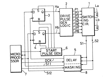
Fig. 1 is a block diagram of a drive circuit for a
sensorless brushless motor according to an embodiment of the
present invention;
Fig. 2 is a circuit diagram showing the switching
circuit of Fig. 1 in more details; ~
Figs. 3A and 3B are plan views of a rotor and a
stator, respectively, of the sensorless brushless motor of
Fig. l;
Figs. 4A-4E represent waveforms of signals present
in the motor of Fig. 1 during operation thereof;
Fig. 5 is a sch~matic diagram showing elements of
the drive circuit of Fig. 1 in more detail; and
Fig. 6 is a waveform chart showing the waveforms
of signals present in the circuit of Fig. 5 during operation
thereof.
DETAILED DESCRIPTION OF PREFERRED EMBODIMENTS
Fig. 1 shows a drive circuit for a sensorless
brushless motor, which in this embodiment is assumed to be
of the two-phase bidirectional energization kind. Such
~ 2781g
motor would then employ a rotor 21 as shown in Fig. 3, which
includes magnets arranged to form eight poles. Similarly,
Fig. 3B is a plan view of a stator for a motor according to
the present invention having two-phase coils Lal, La2 and
Lbl, Lb2 having an electrical angle of 90 and a mechanical
angle of 67.5 formed on the stator base 22. The stator
coils consist of series coils Lal and La2, and Lbl and Lb2,
respectively, which are arranged at electrically in-phase
posîtions, that is! arranged at an integer multiple of an
electrical angle of 360. The winding pitch of each coil is
an electrical angle of 180 or a mechanical angle of 45.
The two-phase coils La and Lb are reciprocally
connected to an energization circui~ by a switching circuit,
shown at 1 in Fig. 1. Such reciprocal connection or
switching is also known as bidirectional switching.
Fig. 2 shows switching circuit 1 of Fig. l in more
detail, in which transistors 11, 12, i3, and 14 are
bridge-connected to the coil La and transistors 15, 16, 17,
and 18 are bridge-connected to coil Lb. Transis~ors 11
through 18 are then turned on every electrical angle of 90
by drive pulses Pl through P8 that are connected to the base
circuits of transistors 11 through 18, respectively.
Accordingly, the ends of each load or coil, La and Lb, are
selectively connected between the positive terminal (~) of a
power supply and ground, thereby providing a driving force
for the motor.
As is well known, during rotation of the motor
sinusoidal induction voltages Ea and Eb with a mutual phase
difference of 90 are generated across coils La and Lb by
--6--
ZS04
--` 27gl9
the rotor magnets. These induced sinusoidal voltages are
shown in Fig. 4A, with voltage Ea shown by a solid line and
voltage Eb shown by a brokPn line, with a 90 phase
difference therebetween. The induction voltages Ea and Eb
are then wave shaped at the zero crossing points, that i5,
at the AC neutral potentials, by comparators 19 and 20,
respectively, having inputs connected to the two ends of
coils La and Lb, respectively. Thus, pulse signals Sl and
S2 (Fig. 4B) having a mutual phase difference of 90
corresponding to the induction voltages Ea and Eb are
obtained as the outputs from comparators 19 and 20. These
pulse signals Sl and S2 are therefore synchronized and
phase-locked with the induction voltages Ea and Eb and their
high and low levels correspond to the respec~ive AC
polarities of the induced voltages, as shown in Fig. 4B.
Thus, the pulse signals Sl and S2 indicate a reference
angular position of the rotor relative.to the stator coils
La and Lb.
Pulse signals Sl and S2 are then fed to a delay
circuit 5 that forms delay clock signal DCK, the leading
edges of which are delayed by a time T from the leading and
trailing edges of signals Sl and S2. The manner in which
clock signal DCR is produced will be shown in detail below.
Thus, the trailing edges of clock signal DCK are
synchronized with signals Sl and S2 and time T corresponds
to an electrical angle of 45. Therefore, an energization
angle having a 90 width with a leading edge corresponding
--7--
-- 27819
to a 45 position from the magnetic pole boundary
corresponding to the reference position of the rotor magnet
21 can be obtained without an angular position sensor, which
is typically re~uired. As will be descxibed hereinbelow,
the time T will be variably controlled by a microprocessor 7
so that it is always kept at an electrical angle ~5, even
if the rotational speed of the motor is varied.
Pulse signals Sl and S2 from switching circuit 1
in Fig. 1 are also fed to a masking circuit 8, which can
optionally share common elements with delay circuit 5.
Masking circuit 8 transforms pulse signals Sl and S2 into
signals Sll and S12, respectively, which are then fed to the
D inputs of D type flip-flops 3 and`4, respectively. The
operation of the masking circuit 8 will be explained
hereinbelow and at this time it is noted that masking
circuit 8 removes the noise pulses included in the pulse
signals Sl and S2 at all portions other than the zero
crossing sections of induction voltage signals Ea and Eb.
Because the noise pulses are based upon the energization
switching of the stator coils, the noises are generated at
specific positions and, thus, the masking position and the
widths of the masking pulses can be controlled by the
control data according to the motor speed from the
microprocessor 7. Flip-flops 3 and 4 receive the delayed
clock signal DCK at the respective clock inputs thereof and,
thus, flip-flops 3 and 4 produce pulse signals Ha and Hb,
delayed by 45 relative to signals Sl and S2, as shown in
. .
~ 5~ 27819
Fig. 4D. These pulse signals Ha and Hb are fed to a drive
pulse generator logic circuit 2 that forms the bidirectional
energization pulses P1 through P8 at every 90 electrical,
which drive signals are shown in Fig. 4E. It is these
pulses P1 through P8 that are utilized to turn on and off
transistors 11 through 18 of Fig. 2 and thereby control the
rotation of the motor. Drive pulse generator logic 2
produces the bidirectional energization pulses P1 through P8
by straight-forward logic processing or encoding so that the
polarities of the magnetic poles of the rotor corres~ond to
the energization polarities during the 90 wide intervals
(45-135 and 225-315) of the magnetic poles opposite
coils La and Lb. In this fashion,;~otational torque in one
direction is generated.
Of course, when rotor magnet 21 is not rotating
and is stopped relative to stator, no voltages will be
induced in the stator coils La and Lb. Accordingly, when it
is desired to start the motor, a star~ pulse signal is
generated by a start pulse generator 6 for a period of time.
Start pulse generator 6 is controlled by microprocessor 7 to
which the motor start switch (not shown) is connected.
Start pulse generator 6 produces start pulse signals
connected to the set and reset terminals of flip-flops 3 and
4, thereby forming two-phase pulse signals similar to pulse
signals Ha and Hb shown in Fig. 4D. Accordingly, when the
motor is started, coils La and Lb are separately excited by
the start signals from start pulse generator 6 and rotor 21
_g_
., . . . .: . .
- : . .... ,~ ..
zs~
27819
is caused to rotate in a predekermined rotational direction
depending ~pon the phase relationship between the start
signals produced by start pulse generator 6 as determined by
microprocessor 7.
Delay circuit 5 of Fig. 1 is shown in more detail
in Fig. 5 as is masking circuit 8. Fig. 6 represents
waveforms found throughout the circuit of Fig. 5 during
operation thereof. More specifically, the induction
voltages Ea and Eb induced respectively in coils La and Lb
are applied to comparators 19 and 20, respectively, and are
so-called zero-cross shaped therein. Comparators 19 and 20
form the pulse signals S1 and S2 also shown in Fig. 6, and
in accordance with typical comparator operation comparators
19 and 20 in addition to detecting induced voltages Ea and
Eb will also detect the noise spikes caused by the stator
coil switching. Such noise spikes are shown at N in
waveforms Ea and Eb in Fig. 6, and because they are
generated at the current switching positions noise will be
found at the corresponding points 45, 135, 225, and 315,
of the signals Ea and Eb. Noise spikes N will be detected
by comparators 19 and 20 and will result in noise pulses Pn
being present in pulse signals Sl and S2. It is these noise
pulses Pn that will be removed by masking circuit 8.
Output S1 from comparator 19 is fed to a leading
edge detector B11 and a trailing edge detector B12, and
output S2 of comparator 20 is fed to a leading edge detector
B21 and a trailing edge detector B22. Thus, signal S1 is
developed into edge pulses S3 and S4 as shown in Fig. 6, and
--10--
z~
^- 2781g
signal S2 is developed into edge pulses S5 and S6, as shown
in Fig. 6. These edge pulses S3, S4, S5, and S6 are fed to
masking AND gates G11, G12, G21, and G22, respectively. As
will be explained hereinbelow, these masking AND gates G11,
G12, G21, and G22 serve to remove the noise pulses Pn, with
the resultant signals being shown in Fig. 6 as S7, S8, S9,
and S10, respectively. Edge pulses S7 and S8 are fed to a
RS flip-flop formed of NOR gates G13 and G14, and edge
pulses S9 and S10 are fed to a second RS flip-flop formed of
NOR gates G23 and G24. These two sets of NOR gates then
produce pulse signals S11 and S12, as shown in Fig. 6. As
may be seen, because of the masking effect pulse signals S11
and S12 have the noise pulses Pn re~oved therefrom at points
other than the zero-cross points of the pulse signals S1 and
S2.
As shown in Fig. 1, signals S11 and S12 are fed to
the clock inputs of D-type flip-flops 3 and 4, which act to
form delayed pulses Sl3 and S14 that correspond to signals
Ha and Hb in Fig. 6, respectively.
Outputs S7, S8, S9, and S10 from masking AND gates
G11, G12, and G21, and G22 are also connected to a multiple
input OR gate G31, so that a pulse signal indicating two
edges of the two-phase signal is formed, that is, the pulses
indicate the Ieading and trailing edges of each of the two
signals, as shown in S16 in Fig. 6. Signal S16 is connected
as a load pulse to terminal LD of a delay counter 26, which
forms the delay circuit 5 shown in Fig. l. The load input
--11--
' ' . ,
s~
27819
of counter 26 then causes control data Do through Dn
corresponding to the rotational speed of the motor to be
input to counter 26 from a data bus 28 of microprocessor 7
through a latch circuit 27. Thereafter, counter 26 counts
the delay clock signals having a predetermined reyuency fed
in from an external clock circuit (not shown) through an OR
gate G33 in response to the load pulse Sl6 based on the load
data. Accordingly, delay counter 26 will generate an
nth-bit (most significant bit) output with the leading edge
occurring after a time T, as shown in waveform S17 of Fig.
6. The frequency of the delay clock signal is based on the
resolution or resolving power, or resolving efficiency, of
counter 260
The locations of load pulses in the waveform Sl6
correspond to electrical angles of 0, 90, 180, and 270
and time T is controlled, that is, lengthened or shortened,
in accordance with the load data, as fed in from
microprocessor 7. Thus, time T is controlled to correspond
to each 45 width between the electrical angles 0 and 45,
between 90 and 135, between 180 and 225, and between
270 and 315 regardless of change in rotational speed of
the motor. In other words,~ at low speed time T is
lengthened and at high speed time T is shortened.
Delay counter 26 then counts the clock signals fed
in through OR gate G33 and upon reaching the most
significant bit Qn the output of counter 26 goes high. This
output of counter 26 is connected to another input of OR
gate G33, thereby blocking the clock input to counter 26.
-12~
.
~ S~)~ 27819
Therefore, the most significant bit output Qn of counter 26,
shown at S17 in Fig. 6, remains at a high level until the
next load pulse S16 is fed to counter 26 to reset the
counter and, thus, the most significant bit level output Qn
falls to a low level. Counter output S17 is also fed to the
clock inputs of flip-flops 3 and 4 as the delayed clock
signal DCK in the circuit of Fig. 1, which signal waveforms
are also shown in Fig. 4C, thereby forming the delayed pulse
signals Ha and Hb, which correspond respectively to signals
S13 and S14 in Fig. 6.
The most significant bit output from delay counter
26 is also fed to a third leading edge detector 25, so that
a pulse representing the leading edge indicated by waveform
S18 in Fig. 6 is formed. Edge pulse S18 represents the
positions at electrical angles of 45, 135, 225 and 315
of respective phases of the two-phase signal. This signal
is also fed to an OR gate G32 that forms an OR output signal
Sl9 from the edge pulse signal S18 and the output puise S16,
which corresponds to 0 and 180 electrical, of multiple
input OR gate G31. Because signal Sl9 is derived from
signal S17, the interval between pulses of signal Sl9 is
lengthened or shortened in accordance with delay time T,
however, the electrical phase angle remains constant at 0,
45, 135, 180, 225, and 31S.
This OR gate output signal Sl9 is f~d as the load
pulse to input LD of a masking counter 29, which comprises
masking circuit 8 of Fig. 1. Masking counter 29 fetches
-13-
. . ,
SO~ 2781g
control data corresponding to the rotational speed o~ the
motor from data bus 28 of microcomputer 7 through a latch
circuit 30, in an operation just as in delay counter 26.
Masking counter 29 counts masking clocks provided by an
external clock circuit (not shown) at a predetermined
frequency by receiving a clock signal through an OR qate G34
at clock input CK. The fre~uency of the masking clock is
determined by the resolution or resolving power, or the
resolving efficiency, of masking counter 29. Thus, masking
counter 29 generates from the most significant bit (MSB)
position Qn a masking pulse signal that falls at angular
positions of 0, 180, 45, 135, and 315, as indicated in
pulse signal S15 in Fig. 6, in which the masking pulse
rises after lapse of a predetermined time period t. Because
the masking clock input to masking counter 29 is connected
through OR gate G34 that has as another input signal MSB
signal S15 from masking counter 29 when MSB signal goes to a
high level, the masking clock is disabled by OR gate G34 and
the counting operation is interrupted until the next load
pulse on signal S19 is fed to masking counter 29.
As described above, the masking width t is varied
in accordance with the rotational speed of the motor as
determined by the microprocessor 7, however, in an alternate
embodiment, the masking width t could assume a fixed value
regardless of the rotational speed of the motor.
The masking pulse S15 is also fed to the masking
AND gates G11, G12, G21, and G22 so that the AND gates are
closed during the low-level period t of the masking pulse
-14-
27815
S15. This has the effect that predetermined periods
immediately following the zero-cross detection at 0 and
180, and at predetermined periods immediately after the
current switching timings at 45, 135, 225, and 315, are
masked, as indicated by the induction voltage waveorms Ea
and Eb in Fig. 6.
Thus, even if low level noise pulses are
superimposed on induced stator voltages Ea and Eb near the
æero-crossing points and the outputs Sl and S2 from
comparators 19 and 20 fluctuate accordingly, once the
leading edge of pulse Sl or S2 is detected, these noise
pulses are ignored by means of the masking signal.
Accordingly, the pulse signals Sll and S12 having a correct
period in which positive and negative half waves of the
induced voltages respectively correspond to the high and low
levels can be obtained. Similarly, because noise spikes
generated at the stator coil switching points can be removed
by masking immediately after the current switching, the
detection at crossing points 0 and 180 are not interfered
with. ~hus, switching timings can be accurately determined
by utilizing the above-described digital delay because the
0 and 180 positions can be accurately detected.
As shown in Fig. 1, the zero-cross detection
signals Sll, and S12, from which any noise interference has
been removed by masking circuit 8, are also fed to
microprocessor 7. The periods of the pulses Sll and S12 are
detected therein 80 that the rotational speed of the motor
-15-
~ ~ 27~19
can be determined. Control data formed by speed detection
is then ou~put onto data bus 28, shown in Fig. 5, in order
to determine the delay time T and the masking width t
corresponding to each 45 interval between 0 and 45,
between 90 and 135, between 1~0 and 225, and between
270 and 315. As described above, because pulses Sll and
S12 having a correct period can be supplied through masking
circuit 8, speed detection can be accurately obtained.
Alternatively, speed detection could be performed by a
frequency generator or a pulse generator attached to the
motor.
Although in the above-described embodiment, the
present invention is utilized with a two-phase bidirectional
energization type sensorless brushless motor, the present
invention finds equal application to a polyphase
unidirectional motor or bidirectional energization type
sensorless brushless motor.
The above description is given on a single
preferred embodiment of the invention, but it will be
apparent that many modifications and variations could be
effected by one s~illed in the art without departing from
the spirit or scope of the novel concepts of the invention,
which should be determined by the appended claims.
-16~