Note: Descriptions are shown in the official language in which they were submitted.
~ ~z~ 3
--1--
A CIRCUIT FOR MEASURING THE DYNAMIC CHARACTERISTICS
OF A PACKAGE FOR HIGH-SPEED INTEGRATED CIRCUITS AND
A METHOD FOR MEASURING SAID DYNAMIC CHARACTERISTICS
BACKGROUND OF THE INVENTION
Field of the Invention
The present invention relates to a device for
determinlng the dynamic performances of an encapsulating
package for a high-speed integrated circuit of the logic
or linear type on gallium arsenide or III-V materials.
The invention is also concerned with a method for testing
the dynamic characterlstics of a package by means of the
; device in accordance with the ~nvention.
Description of the Prior Art
The development of new techniques for
integrated circuits on gallium arsenide (GaAs) or
ternary GaAlAs compounds of the III-V fam~ly, such
circuits~being~designed~for operating frequencies above
l GHæ, calls for ava~lability of encapsulation means
having very high speed performances.
The problem presented by encapsulation of
these so-called subnanosecond integrated circuits
cons~sts~n~assembl~ng a component within a package
20 ~ without thereby affectlng the ~ntrinsic electrical per-
formances of the encapsulated integrated circuit. In
the great ma]ority of~nstances, packages for this type
of~integrated circult conslst of flat c~ramic cas~ or
.
`: : -' ' : '
,
: . .
,
-2-
so-called Plat pack8. Thus French patent
N 2 529 385 filed in the name of the present Applicant
discloses a flat pack having external connections
consisting entirely of impedance-matched microstrips.
This package constitutes a highly advantageous improve-
ment in the encapsulation of high-speed circuits.
The object of the present invention i9 to pro-
vide a device and a method which permit measurement in
situ (that is to say under real conditions of operation
of~integrated circuits) of the electrical performances
., ~
of packages which operate at very high frequency such
as those described in the patent cited earlier.
SUMMARY OF THE INVENTION
The device in accordance with the invention
consists of a set o two identical amplifiers or
preferably three identical amplifiers integrated on one
and the same chip of semiconductor material and
connected in parallel, each amplifier being provided
with an input terminal and an output terminal which are
independent of the input and output terminals of the
other amplifiers. Two amplifiers are integrated in
parallel with adjacent input terminals and adjacent
output terminals and two amplifiers are integrated in
top-to-tail relation.
The method consists in mounting said amplifier
.
.
`-~ J z~Z~13
--3--
chip within the package whose characteristics are to be
measured at very high speed, and in measuring the
coefficients of transmission of the package between
external access connect.ions selected in pairs on
different sides of the package.
More specifically, the invention relates to a
circuit for measuring the dynamic characteristics of an
encapsulating package for high-speed integrated circuits
~1 GHz), said measuring circuit being distinguished by
the fact that it includes on a supporting substrate of
semiconductor material at least two identical amplifiers
in which :
- the input impedance corresponds to the input impedance
of the integrated circuit to be encapsulated within the
package,
- the output impedance is identical with the output
impedance of said integrated circuit,
- the power supplies are separate and the implantation
pattern has a very wide spacing in order to ensure that
there is no electrical coupling,
- the metallizations of the input and output terminals
are located on the edges of the substrate in order to
minimize the length of the external connections, said
edges being selected opposite to the edges of the en-
capsulating package which support external accessconnections.
~c3zs~3
--4--
BRIEF DESCRIPTION OF THE DRAWINGS
FIGS. 1 and 2 illustrate two chips carrying
amplifiers which are mounted in parallel and in anti-
parallel, in accordance with the invention.
FIG. 3 illustrates a chip carrying three
amplifiers including one amplifier mounted in anti-
parallel and constituting an alternative embodiment of
the invention with respect to FIGS. 1 and 2.
FIG. 4 is a diagram of the method in accord-
ance with the invention for measuritlg the coefficient
of transmission of a package.
FIG. 5 is a diagram of the method in accordance
with the invention for measuring the coefficient of
coupling between two access connections employed as
inputs.
FIG. 6 is a diagram of the method in accordance
with the invention for measuring the coefficient of
coupling between two access connections employed as out-
puts.
FIG. 7 is a diagram of the method in accordance
with the invention for measuring the coefficient of
coupling between an access connection employed as input
and an access connection employed as output, these
connections being placed side by side.
FIG. 8 is a diagram of the method ln accordance
with the invention for measuring the coefficlent of
--5--
coupling between an access connection employed as
output and an access connection employed as input,
these connections being separated by a screen.
DETAILED DESCRIPTION OF THE INVENTION
Apart from mechanical performances such as
hermetic sealing or heat-removal capacity, the quality
of a package employed at high frequencies is directly
related to its ability to carry high-speed signals
from the external environment (supporting board) to the
integrated circuit chip. This can be summarized by two
electrical quality criteria :
- electrical transmission of the access connections,
- electrical decoupling between the different access
connections.
The first criterion characterizes the low
degradation of the travellng signals. The second
criterion characterizes the low crosstalk between-
access connections which may be the cause of undesirable
parasitic signals.
Measurement of these two parameters in real
value is extremely difficult since, in order to judge the
quality of connections which have been made, this measure-
ment would entail the need to collect the electrical
quantities from the integrated circuit itself.
The device in accordance with the invention
makes it possible to carry out quantitative measurements
.
~' ` ~, ' ' ' ,', .
9ZS13
--6--
of the dynamic performances of a package, primarily in
terms of coupling in a real environment.
This parameter is a very important datum,
especially in the field of encapsulation of signal-
processing linear integrated circuits which make use ofvery precise analog quantities having small amplitudes
together with clock signals having high levels and a
frequency which can be higher than 1 GHz.
A full analysis of specifications of packages
c'alls for availability of two types of circuits as
illustrated schematically in FIGS. 1 and 2.
In a first case as shown in FIG. 1, two
amplifiers 4 and 5 are integrated on a chip 1 of semi-
conductor material in accordance with an implantation
pattern or layout such that they are mounted in parallel.
Thus the two input terminals are in side-by-side relation
on the same edge of the substrate 1 whilst the two out-
put terminals are located side-by-side on an opposite
edge of the substrate.
In a second case as shown in FIG. 2, two
amplifiers 5 and 6 are integrated on a chip 2 of semi-
conductor material but are located in this instance in an
antiparallel or top-to-tail arrangement. Thus the input
terminal of the amplifier 5 is adjacent on one edge of
the substrate 2 to the output terminal of the amplifier 6
and the output terminal of the amplifier 5 is adjacent on
_7_ ~ZS13
an opposite edge of the substrate to the input terminal
of the amplifier 6.
The use of these two types of circuit will be
explained hereinafter and corresponds to measurements on
access connections located on two opposite edges of a
package. If measurements are to be made on access
connections located on two adjacent edges of a package
having peripheral connections, the implantation patterns
of the amplifiers are such that the input and output
terminals are on two adjacent edges of the substrate 1
or 2 so as to ensure that the metallic strip connections
between the circuit position and the external connections
are as short as possible in order to avoid any introduc-
tion of new elements in the measurement of the charac-
teristics of a package.
Should it be necessary to employ both types ofcircuit as illustrated in FIGS. 1 and 2, which depends
on the measurements to be made on a package, the circuit
illustrated in FIG. 3 offers an effective solution.
Three amplifiers 4, 5 and 6 are implanted into a
substrate 3 of semiconductor material and, taken in
pairs, correspond to the circuits aforesaid as follows :
- the amplifiers 4 and 5 are mounted in parallel as in
FIG. 1,
- the amplifiers 5 and 6 are mounted in antiparallel as
in FIG. 2.
`~` lZ92S13
--8--
It will readily be apparent that, in the three
configurations considered, the amplifiers are identical
and their basic design as well as the materials selected
(GaAs, AlGaAs, ... etc.) make it possible to operate at
frequencies at least as high as those at which the
package is to be measured.
Moreover, in view of the fact that an amplifier
is often limited to a single transistor at microwave
frequencies, the two or three amplifiers can advant-
ageously be implanted in the chip of a microwaveintegrated circuit which is encapsulated in the package
whose characteristics are to be measured.
In all cases, the two or three amplifiers of
the measuring circuits meet the following specifications:
- inverting or non-inverting linear transfer function
(vs = A ve),
- input impedance corresponding to the input impedance
of the devices of the logic family to be encapsulated,
- output impedance identical with the output impedance
of the circu~ts of~the logic family to be encapsulated.
All precautions are taken in regard to
implantation of these circuits with a view to ensuring
that the internal electrical coupling is zero, viz:
- spaced;signal lines (vefy loose implantation),
- separate power supplies for the amplifiers.
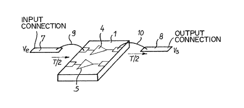
~ ~ FIG. 4 is a diagram representing the method of
:
9;~13
`` 9 .
measurement of the coefficien~ of transmis~ion o a
package. For the sake of enhanced simplicity, this
figure shows only the following circui~ elements :
- the chip 1 of the measuring circuit,
- two package access connections 7 and 8,
- wire or strip connections 9 and 10 between the
amplifier 4 and the connections 7 and 8.
The amplifier 5 is not employed for measuring
the coefficient of transmission.
Let the reference 7 designate the input
connection and the reference 8 designate the output
connection of the package : in the package of French
patent 2 529 385 these connections are
microstrips adapted to the utilization frequency.
Let the reference T designate the coefficient
of transmlssion of the package : this coefficient is
divided into T/2 at the input of the package and T/2 at
the output of said package. It is the result of
parasitic elements such as capacitance, inductance of
the strips 9 and 10, leakages in dielectrics, and so on.
If a known electric signal Ve such as a pulse
train is sent to the input connection 7, it is possible
to measure a signal Vs on the output connection 8 which
is of the form
VS = A . Ve . T
where A is the gain of the amplifier 4.
. .
~ ~Z~Z~:~3
--10--
The coefficient of transmission T
T = (l/A) . (Vs/Ve)
is thus measured at the utilization frequency of the
package.
The value T being known, it is possible to
measure the coupling between two adjacent access
connections employed as inputs. As shown in FIG. 5, a
measuring circuit in accordance with FIG. 1 or FIG. 3 is
so arranged that the input of the first amplifier 4 is
connected by means of a strip 9 to the input connection
7 and its output is not connected. The input of the
amplifier 5 which is parallel to the amplifier 4 is
connected to an external connection 11 which is adjacent
to the connection 7. The output of said amplifier is
connected to an external connection 12 on one edge of
the casing opposite to the edge which supports the input
connections 7 and 11.
An input signal Ve is applied to the connection
7. Thus the amplifier 5 delivers the output signal Vs if
a coupling CE/E exists between the inputs 7 and 11.
VS = CE/E A . Ve
ElE (l/A) . (l/T) . (Vs/V )
In order to measure the coupling coefficient
between two adjacent output connections, the wiring
scheme of FIG. 6 is adopted. In a measuring circuit as
shown in FIG. 1 or in FIG. 3, a first amplifier 4 i.s
-` 12~S13
connected by means of strips 9 and 10 to the input
connection 7 and to the first output connection 8. The
second amplifier 5 which is paral:lel to the first
amplifier 4 has a grounded input and an output connected
to a second output connection 12 which is adjacent to
the first output 8.
An input signal Ve is applied to the connection
7. Thus the amplifier 5 delivers an output signal Vs2 if
there is a coupling CS/s with the signal Vsl between the
two output connections 8 and 12.
S2 CS/S VSl = Cs/s A . Ve . T
S/S (l/A) . (l/T) . Vs2/Ve
If two adjacent connections on the same edge
of the package are employed in one case at the input and
in the other case at the output, the wiring scheme of
FIG. 7 is adopted for determining the input/output
coupling coefficient CE/S.
The measuring circuit employed is that of
FIG. 2 or the portion of FIG. 3 in which two amplifiers
5 and 6 are moun~.ed in antiparallel or top-to-tail
relation.
The input of the amplifier 5 is connected to
the input connection 11 and the output of said amplifier
is not connected. The input of the amplifier 6 is
connected to ground and its output is connected to the
connectlon 15 which is adjacent to the input connection
11 .
:
.~ .
-12- ~Z~3ZS13
In this case, coupling takes place directly
between the two input-output microstrips 11 and 15.
Since the microstrips 12 and 17 located on the opposite
edge of the package are not connected to anything, the
gain A of the amplifiers and the coefficient of trans-
mission T of the package are of no practical use. The
output signal Vs is directly derived from the lnput
signal Ve by the coupling CE/S between the connections
11 and 15 :
Vs = CE/S Ve
CE/s = (VS/Ve)
Finally, FIG. 8 illustrates the case of
measurement of the coupling coefficient between an output
and an input which are located on the same edge of the
package but separated by a screen constituted by one or
two grounded connections 19 and 20.
. The measuring circuit employed is that of
FIG. 2 or of FIG. 3 in which two amplifiers 5 and 6 are
implanted in antiparallel or top-to-tail relation. The
amplifier 5 is connected to two connections 11 and 12
and the amplifier 6 is connected to two connections 15
and 16. Thus the adjacent connections 12 and 16 on one
edge of the package are coupled and the connections 11
and 15 on another edge of the package are separated
by the screen of connections 19 and 20. Should a
coupling exist between the connections 11 and 15, said
l~ZS13
-13-
coupling is established via the connections 12 and 16.
In the case shown in FIG. 4, we have :
Vs2 = A Ve2
but the signal Ve2 on the connection 16 exists only
because there is a coupling CS/E with the signal Vsl on
the connection 12 :
e2 CS/E VSl = CS/E A Vel T
therefore
S2 A . T Cs/E A Vel T
10 ~S/E = l/(A T ) (VS2/Vel)
FIGS. 4 to 8 show a two-amplifier circuit in
accordance with FIGS. 1 and 2 and remain valid if,
instead of mounting two circuits in a package for the
dynamic measurements to be performed on this latter,
only one circuit is mounted as in FIG. 3, the amplifiers
of which are employed in pairs according to the type of
measurement to be carried out.
When a package is defined in dynamic
performance, the measuring circuit or circuits can be
unsoldered and the utilization integrated circuit is
soldered within the package.
The field of application of the invention
extends to all areas of high-speed electronics in which
encapsulation of families of circuits having very high
performances is a matter of particular concern. The
scope of the present invention in no way excludes new
~9;~13
-14-
generations of silicon integrated circuits having
highly advantageous speed characteristics and
specifications.
:
.