Note: Descriptions are shown in the official language in which they were submitted.
25i~3
METHOD AND ARRANGEMENT FOR A SIGMA DELTA CONVERTER
FOR BANDPASS SIGNALS
10 RELATED APPLICATIONS
This case is related to two U.S. patents. The first
is U.S. patent number 4,893,316, entitled All Digital
Radio Frequency Receiver, issued on January 9, 1990, and
the second is U.S. patent number 4,811,362, entitled Low
Power Digital Receiver, issued on March 7, 1989. Both of
these patents are owned by the owner of the present
application.
BACKGROUND OF THE INVENTION
The present invention relates generally to analog-to-
20 digital (AjD) converters, and more particularly to sigmadelta A/D converters. It is generally known that an analog signal can be
converted to a digital signal (or vice-versa) when the
sampling frequency, f~, of general A/D (or D/A)
25 converters is selected to be about twice the signal
frequency bandwidth, fBW- This relationship between
the sampling frequency, fs, and the signal frequency
bandwidth, fBW~ is the ~ami}iar Nyquist's theorem.
In conventional oversampling A/D converters, the
30 sampling frequency, fs~ is set higher than twice the
signal frequency bandwidth, ~BW~ which would be
establIshed by Nyquist's theorem, in order to achieve
~'
- 2 -
improved conversion precision by reducing conversion
errors. Thus, when a sampled analog input signal is
quantized in~o a digital signal in a conventional A/D
conversion stage, a conversion exror ~or quantization
error~ occurs which is the difference between the analog
input voltage and a digital ou~put (quantized) step
voltage. Such quantization error is given as a random
value falling between an amplitude range of ~ Vq/2 and
~Vq/2 with respect to a minimum quantized step voltage,
10 Vq.
As a result, the frequency spectrum of the
quantization noise produced by such quantization errors
is spread in a uniform manner over the interval from 0 Hz
to half the sampling rate, or fs/2. Filtering is then
15 used to eliminate the noise power outside of the desired
signal bandwidth.
The well known sigma delta converter uses feedback
to shape the quantization noise into a highpass
characteristic. As a result, the quantization error is
20 suppressed most at low frequencies, where the loop gain
is highest. However, because the total root-mean-square
(RMSj quantization error is constant and ultimately
limited by the D/A conversion step size, the reduction in
tha low freguency quantization noise which effects the
25 reduced quantization error is therefore accompanied by an
increase in quantization noise at high frequencies.
Hence, digital filters are generally used following the
sigma delta converter to attenuate this
undesired quantization noiss at high frequencies, namely
30 those above the cutoff frequency of one or more
integrator stages within the sigma delta converter.
Furthermore, it i8 generally known that if additonal
conversion precision is required beyond that available
from a single integration, first-order sigma delta
35 converter, a second integration stage can be incorporated
to effect a second-order sigma delta converter. Such
sigma delta A/D converters are well known for their
.
-- 3 --
ability to reduce inband noise power within a lowpass
characteristic, and hence such converters operate best
upon analog input signals operating at baseband. A
baseband ~ignal is defined here as one having a lowpass
characteristic. Examples of ways to arrive at a baseband
signal include down-converting or demodulating an RF
signal with various known detection methods.
One application of particular interest for sigma
delta A/D converters is in mobile radios utilized in
10 modern communication systems. In such applications, a
baseband signal can be provided when a received signal is
down-converted to an intermediate frequency (IF) signal
having a center frequency equal to zero Hertz (0 Hz), or
when a signal, such as an IF signal, is detected to
15 produce a baseband signal (i.e., falling between O Hz and
an upper cutoff frequency; fc~ having a bandwidth
fBW)~ with the carrier signal removed. Carrier signal
is defined broadly herein as referring to the center
frequency of RF signals or IF signals.
However, several disadvantages become apparent when
attempting to convert a baseband analog signal to a
digital signal utilizing a conventional sigma delta A/D
converter having a lowpass characteristic. Namely, there
is an inherent ambiguity in di tinguishing between
25 signals occuring at O Hz and DC offset voltages existing
in active 6tages within the sigma delta A/D converter.
Also, the unavoidable crosstalk between the in-phase and
quadrature (or I/Q) channels of a zero-IF receiver can
mix undesired out of ban~ signals into the desired
30 passband. ~ further disadvantage is that the noise
present in active circuits is always higher at low
frequencies due to flicker or 1/f noise. As a result,
there are serious limi~ations placed upon the ultimate
signal-to-noise ratio, and hence the dynamic range, that
35 can be obtained in a given mobile radio application.
Such limitations have been only partially overcome by
: .
,~ .
`
:
various known arrangements which, at the expense of
greater complexity, attempt to deal with the ambiguity
created by the DC o~fset component, I/Q cros~talk, and
added noi~e.
Accordingly, there exists a need for an improved,
yet simpler, sigma delta A/D converter that provides
greater dynamic range while avoiding the ambiguities,
undesired signals, and added noise caused by attempting
to convert signals occuring at 0 Hz. This permits the
signal processing functions occuring thereafter to be
performed digitally, including the reguired mixing,
filtering, and demodulating functions. Such need exists
for many applications requiring relatively fast, analog-
to-digital conversion with low quantization error,
including radio receiver applications.
SUMMARY OF THE INVENTION
It is an object of the present invention to provide
a sigma delta converter which overcomes the foregoing
deficiencies by converting an analog signal to a digital
signal with improved signal-to-noise ratio performance
and with minimal quantization error, while avoiding the
ambiguity of signals falling at zero Hertz (0 Hz).
It is a further ob;ect of the present invention to
provide a sigma delta converter of the foregoing type
which operates upon bandpass signals by converting an
input signal having a non-zero freguency carrier or
suppressed carrier with modulation thereon from an analog
signal to a digital signal.
In practicing the invention, one embodiment
contemplates a second order sigma delta converter for
3',~
bandpass signals, suitable for use in mobile radio
applications, that includes at least one bandpass filter,
an N-level quantizer, an N-level digital-to-analog (D/A)
converter, and a direct current (DC) feedback network.
In another embodiment, a fourth order sigma delta
converter for bandpass signals is disclosed which further
includes a second single pole bandpass filter having an
amplifier. Each of these embodiments achieves analog-to-
digital conversion of a bandpass signal having a non-zero
10 frequency carrier or supressed carrier with improved
signal-to-noise ratio performance and with minimal
quantization error. As a result, the sigma delta
conversion occurs earlier in a radio receiver chain and a
dynamic range of about 95-98 dB is achieved.
BRIEF DESCRIPTION OF THE DRAWINGS
Referring to the drawings, wherein like reference
numerals indicate like elements in these several figures,
and in which:
Fig. 1 is a simplified blocked diagram of a radio
receiver having a front end and having one embodiment of
the sigma delta converter for bandpass signals according
to the present invention.
Fig. 2 is a detailed schematic diagram of the sigma
25 delta converter depicted in Fig. 1.
Fig. 3 is a frequency spectral diagram
representative of the Nyquist bandwidth in the vicinity
of a non-zero frequency carrier for the sigma delta
converter depicted in Fig. 2.
DETAILED DESCRIP~rION OF THE PREFERRED EMBODIMEN~r
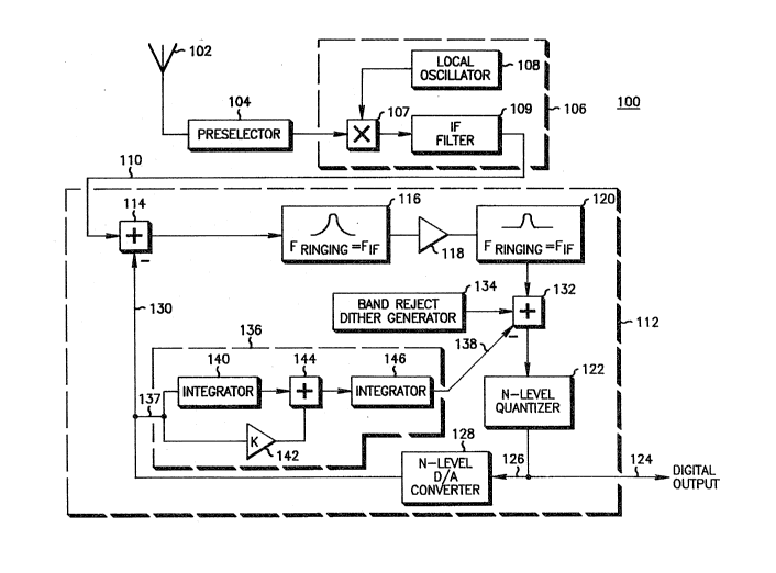
Referring now to the figures, Fig. 1 shows a radio
receiver front end and a sigma delta converter
constructed and arranged to receive an analog input
signal and convert it to a digital output signal. As
shown, the radio receiver includes an antenna 102, a
preselector stage 104, which couples to a receiver front
-- 6 --
end 106 having a mixer 107, a local oscillator 108, and
an intermediate frequency (IF) ~ilter los, as well as an
output line 110.
Next, Fig. 1 at 112 depicts a simpli~ied block
diagram of the si~ma delta converter for bandpass signals
in accordance with the present invention. Sigma delta
converter 112 includes a first summing node 114, coupled
to a single pole bandpass filter 116, which is second-
order and which has a ringing frequ~ncy set equal to the
IF frequency presented from the output of front end 106
via output line 110. Although the ringing frequency,
which is slightly different than the resonant frequ2ncy,
is utilized because of the sampling nature of the sigma-
delta conversion process, these terms will be used
interchangeably ~or the center frequency.
The output of bandpass filter 116 couples to an IF
ampli~ier 118, having IF gain of approximately 40 dB.
Next, the output of IF amplifier 118 couples to another
single pole bandpass filter 120, which is second-order
and which has a ringing frequency set equal to the IF
frequency. Filter 120 also include~ dual-zero phase
compensation to be discussed later. The output of
bandpass ~ilter 120 couples to a second summing node 132
which, in turn, couples to the input o~ an N-level
quantizer stage 122 to provide the digital ouput signal
at node 124, as shown, to an appropriate digital
processing circuit (not shown). The output from N-level
quantizer 122 also couples, via line 1~6, to the input of
N-level digital-to-analog (D/A) converter stage 128, as
shown. The output o~ D/A converter stage 128 couples,
via line 130, to the minu~ input of the first summing
node 114, as shown.
An optional band reject dither generator 134 may be
included within the sigma delta converter of the present
invention and coupled to the second summing node 132, as
-- 7 --
shown. The use of dither to randomize guantization
errors and therefore smooth the ~requency spectrum of the
error is well known to those skilled in the art.
A direct current (DC) feedback network 136 i~ also
provided within the ~igma delta converter that helps
minimize ~C offset voltages. Feedback network 136 has an
input port 137, which is fed by the output of D/A
converter 128, as well as an output port 138, which
couples to a minus input of second summing node 132. The
10 DC feedback network input port 137 couples to a first
integrator stage 140, as well as to an amplification
stage 142, as shown. The outputs of each of integrator
140 and constant gain amplifier 142 couple to an included
summing node 144, which drives the input of a second
15 integrator 146, as shown .
The sigma delta converter shown in block diagram
form in Fig. 1 at 112 i8 referred to as ~ourth order
because it includes two bandpass filters, 116 and 120,
each being second-order. A second order sigma delta
20 conver~er is arranged by deleting the second bandpass
filter 120 and coupling the output of IF amplifier 118
directly to the summing node 132. Also, although shown
generally in block diagram form as comprised o~ single
ended component~, namely those with a single active line
25 with respect to a common ground, the preferred embodiment
is constructed utilizing elements having dual
differQntial leads with respect to a common or chassis
ground so that betker noise immunity is provided, and is
given in the next figure. The two-fold symmetry provided
30 by this dual differential embodiment provides additional
and substantial advantayes when quantizer 122 and D/A
converter 128 have two levels ~1 ~it). In this case, the
signal-to-noise ratio will not degrade as long as each of
these two levels produce equal but opposite responses
35 throughout the converter. Unequal rise and fall times of
signals in a single-ended embodiment will
.
19
-- 8 --
degrade performance because it Will weight one level
higher than the other. One can minimize this degradation
by making the rise and fall times extremely fast, but at
the expense o~ substantially increased power
5 requirements. In a fully differential imp~ementation,
rise and fall times can di~fer and performance will not
be degraded as long as each side of the dif~erential
circuits behave identically. Hence, power requirements
are substantially reduced.
Referring next to Fig. 2, a more detailed schematic
diagram of the fourth order sigma delta converter 112
introduced in Fig. 1 is depicted at 200 having IF signal
input 110 and a two-level digital output 124 having
differential leads 124A and 124B. First summing node 114
15 is represented by points 114A and 114B, as shown.
Following summing node 114 is bandpass filter 116,
depicted in dashed outline form. It includes a resistor
202 to set the bandwidth as well as an inductor 204 and
capacitors 206 and 208 which cooperate to provide a
20 damped sinusoidal impulse response with a ringing
frequency set equal to the IF frequency.
Next, IF ampli~ier 118 follows bandpass filter 116
and includes dual differential inputs and outputs.
Amplifier 118 produces a current at its outputs
25 proportional to the voltage difference between its
inputs. Then, a second bandpass filter 120 follows
amplifier 118 and includes resistor 210 in a parallel
combination with inductor 212 and the series connection
of capacitors 214 and 216 which cooperate to provide a
30 ringing frequency set equal to the IF frequency similar
to filter 116. Those ~killed in the art will recognize
that the LC resonators shown in bandpass filters 116 and
120 can also be implemented in known ceramic or other
piezoelectric technologies. Alternatively, the inductors
35 204 and 212 can be replaced by active circuits, such as
gyrators.
S15~
g
Filter 120 also includes dual zero phase
compensation via resistors 218 and 21g to provide
sufficient phase margin for this fourth order sigma delta
converter for frequencies below or above resonance. This
dual zero phase compensation provides a network that
ensures stable operation by having the total loop phase
lead or phase lag less than 180 degrees at frequencies
below that of a "zero signal idle pattern". The zero
signal idle pattern for the fourth order bandpass sigma
delta converter during no signal and no dither operation
consists of a pattern as follows: ...11001100... for this
fourth order system. Following filter 120 is summing
node 132 which comprises summing amplifier 220 and
resistors 221A and 221B which couple to points 132A and
132B. Summing amplifier 220 produces a differential
current at its outputs proportional to the voltage
difference between its inputs.
N-level quantizer 122 i5 depicted as a two level A/D
converter 122 which includes a latching comparator 222
driving a master slave (M-S) D type flip-flop that is
driven by a clock signal, via input line 226, from a
clock oscillator (not shown). This clock signal, which
may be supplied from a source such as a microcontroller
clock oscillator, determines the sampling rate for the
overall sigma delta converter. In this fourth order
embodiment, a sampling frequency of about 14.4 MHz was
chosen, wh$ch i5 32 times the IF frequency, namely 450
KHz. Time delay 228 is included to ensure that the
output of the latching comparator 222 reaches its full
value be~ore it is transferred to flip-flop 224. Too
short of a delay introduces errors due to insufficient
level, whereas too long of a delay creates extra phase
shift that cau es the loop to go unstable~ The output of
this two level A/D converter 122 provides the 1 bit (2-
level) digital output in differential form via lines 124A
and 124B, and is fed back to a 2-level D/A converter 128,
-- 10 --
which has a constant current sink (or source) 230, having
a constant value of current = I1, driving analog switch
232 controlled by the 1-bit digital outpuk signal. The
resulting output follows lines 130A and 130B back to the
first summing node 114, represented by points 114A and
114B, to complete the feedback loop.
Also included within sigma delta converter 200 is DC
feadback network 136' and another 2-level D/A converter
128' that has its own constant current sink (or source)
10 234, having current = 2I2, analog switch 236, and
constant current source 238, having a constant value of
current = I2. DC feedback network 136' further
includes capacitor 239 across summing nodes 144A and
144B, representing summing node 144, for developing a
15 voltage that is fed to the voltage controlled inputs of
amplifier 146 having current mode output lines 138A and
138B that drive the second summing node 132, represented
by points 132A and 132B. Thus, it is clear that DC
feedback network 136i represents a simplified version of
20 the DC feedback network 136 depicted earlier in Fig. 1,
in that the first integrator stage 140 and amplifier 142
have been omitted.
Turning next to Fig. 3, a frequency spectral diagram
is shown that simulates the performance of the
25 arrangement previously given in Fig. 2. This frequency
spectral diagram shows the characteristic suppre~sion of
noise 302 within the passband response of the bandpass
filters and especially near the vicinity of the center,
or carrier, frequency 304. The simulated conditions were
30 for a fourth order sigma delta converter for bandpass
signals utilizing a first and a second two pole bandpass
filter and having a sampling frequency equal to 16 times
the ringing frequency (or center frequency) of the
filters. Each of the two bandpass filters had a quality
35 factor, (or Q), equal to 40, and the ultimate stopband
response of filter 120 was set to .01 or -40 dB by the
dual zero phase compensation. [OdB, which is off the
vertical scale of figure 3, corresponds to the maximum
signal level at the 1 bit output 124.] As can be seen,
for out of band signals, the average noise level 302 is
approximately -40 dB on the vertical magnitude axis,
whereas for signals very nearly equal to the center
frequency 304 of the sigma delta converter's passband, an
improved signal-to-noise ratio per~ormance has allowed a
dynamic range of approximately 95 to 98 dB to be
10 achieved. Although this simulation was run for a center
frequency of 50 Hz, the circuitry given in Fig. 2
operates well at higher IF frequencies, including an IF
frequency of approximately 450 KH~.
~s inferred by the spec~ral diagram of Fig. 3, tha
sigma delta converter for bandpass signals according to
the present invention offers improved performance at the
IF passband frequencies over other known-converters that
operate satisfactorily only for baseband signals. That
is, the present method and arrangement provides
performance 82 dB better in the desired IF passband than
what would be achieved if a conventional sigma delta
converter were utilized that operated at the same
sampling frequencie~ which are much higher than those
required for baseband signals. Although a conventional
converter will show less degradation if the IF passband
frequency is lowered, image and other known spurious
responses prevent any substantial improvement to be
achieved by the use of this method.
The clock input signal provided to line 226 for the
sigma delta converter according to the present invention
- requires a minimum sampllng rate o~ at least four times
the IF ~requency for the disclosed fourth order system in
order that the frequencies o~ the idle pattern be
removable ~rom the passband. In the example given above,
35 practical sampling rates should be at least double these
minimum rates in order to ease ~iltsring requirements and
. . ,
Z~ ~9
~ ~.
- 12 -
improve stability of the sigma delta converter
arrangement. Moreover, for a simpler second order system
in which only a single pole bandpass filter is utilized,
the minimum sampling rate must be greater than or equal
to two times the RF frequency in order that the idle
pattern (namely... 101010...) ~or such a second order
system be removable from the passband. Furthermore, it
will be apparent to those skilled in the art that IF
amplifier 118 is neceRsary only because an ideal
quantizer, or N-level A/D converter 122 is not presently
available. ~he practical two level quantizer 122
depicted in Fig. 2 has limited gain in its linear region
at a given sampling rate, and therefore the noise figure
of this device is relatively poor. Thus IF amplifier 118
is required in the location shown in order to provide low
noise takeover gain to improve the overall noise figure,
and to reduce the quantization errors caused by finite
gain within the two level quantizer 122.
As a result, each of the above arrangements is able
to overcome the limitations of the known art. That is,
these embodiments provide a sigma delta converter for
bandpass signals tha~ significantly raduces noise most at
- the desired IF ~requency. These embodiments, therefore,
provide minimal signal-to-noise ratio degradation and
quantization error, while simplifying the sigma delta
analog-to-digital conversion of bandpass signals without
the DC of~set problems common in conventional zero-IF
arrangements.
Although the arrangements of the present invention
fully disclose many of the intended advantages, it is to
be understood that various changes and modifications may
be made by tho~e skilled in the art, without departing
from the scope of the above invention.
,