Note: Descriptions are shown in the official language in which they were submitted.
Description
Precision 50% Duty Cycle Controller
Technical Field
This invention relates to demodulation and, in
particular, to a precision 50% duty cycle controller.
Background Art
For modulated signals having a high second
harmonic content it is desirable to reject the unwanted
components using a properly phase shifted chopper
signal with no second harmonic as the baseband
demodulation signal. A precision squarewave meets this
requirement.
For example, in a serrodyne nulled fiber optic
gyro, the signal being nulled is present along with a
much larger second harmonic bias at twice the frequency
of an AC carrier ("dithering") bias injected in the
loop in order to reduce sensitivity to DC fluctuations.
Designs requiring a demodulator to reject second
harmonics typically utilize "divide-by-two" schemes to
create a precision 50% duty cycle. With
"divide-by-two" techniques performance is limited to
th~t of the rise and fall time capability of thé
divide-by-two circuit. This works fairly well, but the
signal applied to the "divide-by-two" network must be
derived using phase-locked-loop up-converter
techniques. This necessarily introduces aircuit
complexities associated with suah techniques.
-- 1 --
H1905-GC
,
';`
: .~.
Disclosure of the Invention
The object of the present inven~ion is ~o provide
a precision 50~ duty cycle controller.
According to the present invention, a sinusoidal
re~erence wave at a frequency much less than a carrier
frequency but referenced thereto is applied to an open
loop operational amplifier which is overdriven thereby
to provide a trapezoidal waveform to a high speed,
differential transistor pair which provides a
squarewave whose duty cycle is regulated at 50% by
varying the threshold at which the differential pair
switches. The squarewave is then used as a
second-harmonic-free demodulating signal for
demodulating a carrier predominated by the same second
harmonic.
The fundamental premise is that if the amplitude
levels of the squarewave are known to a high degree of
accuracy, and they are equal in the positive and
negative directions, then the average value is zero
only for a 50% duty cycle.
A current regulator generates a selected current
which is switched from one side to the other of the
differential pair by the trapezoidal waveform. The
voltage excursions are controlled in equal amounts
above and below zero by selecting the resistive values
in the collector circuits of the di~ferential pair to
be of a magnitude which will accomplish that end.
The average value of the resulting squarewave is
regulated to zero by integrating the voltage at the
Z~Z3
output of one of the collectors of the differentia].
pair and varying the threshold at the base of the
other transistor to obtain a 50% duty cycle.
The present invention provides a closed loop
regulation of the duty cycle that results in an
absolute assurance of creating a 50% duty cycle for
demodulation purposes.
In accordance with a particular embodiment
of the invention there is provided a duty cycle
controller, comprising:
an amplifier, responsive to a sinusoidal
signal, for providing a trapezoidal signal;
a differential transistor pair having equal
collector circuit resistances, responsive to a supply
voltage and to said trapezoidal signal, for providing
a current alternatively through each transi.stor of
said differential pair and for providing square waves
at said collectors;
a current regulator, responsive to said
current, for regulating said current in proportion to
said supply voltage divided by half said collector
resistance; and
an integrator, responsive to a voltage on
the collector of one of the transistors of said
differential pair, for providing a signal to the base
of the other one of said differential pair for
regulating the average value of said square waves to
zero.
These and other objects, features and
advantages of the present invention will become more
apparent in light of the following detailed descrip-
tion of a best mode embodiment thereof, as illustrated
in the accompanying drawing.
~Z~23
Brief Description of the Drawing
Fig. 1 is a simplified block diagrarn illus-
tration of a precision demodulation circuit for use
with a duty cycle controller, according to the present
invention; and
Fig. 2 is a simplified schematic diagram of
a precision 50~ duty cycle controller, according to
the present invention.
Best Mode for Carrying out the Invention
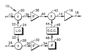
Referring first to Fig. 1, a demodulation
circuit 10 for use by way of example and not limitation
with a duty cycle controller, according to the present
invention, is shown in simplified block diagram form.
The demodulation circuit 10 is generally applicable to
demodulation of any modulated signal but will be
described in terms of a modulated signal on a line 12
being a modulated ("dithered") Sagnac phase shift
- 3a -
:, ...
: '
.
. , .,
Z3
signal from a fiber optic gyro. Such a signal has
normally been modulated in order to reduce
sensitivities to DC changes, such as the light source
intensity. The signal on the line 12 must be
S demodulated and provided as a pure Sagnac phase shift
signal on a line 14 which may then be amplified in an
amplifier 16 and provided on a line 18 as an amplified,
demodulated Sagnac phase shift output signal on line
18. Such a demodulated signal would normally be used
to null the Sagnac phase shift in a manner known in the
art.
The demodulation circuit 10, according to the
present invention, comprises a mixer 20 responsive to a
squarewave signal on a line 22 from a local oscillator
24 operating at a selected frequency, for example,
slightly below, e.g., lOkHz below, the gyro dither
frequency of, e.g., 500 kilohertz.
A reference signal on a line 26 has a frequency
equal to the dither frequency, i.e., 500 kilohertz and
in phase therewith, being derived from the same dither
drive signal source (not shown) as that from which the
dither carrier component of the signal on line 12 is
ultimately derived. It also is mixed with the local
oscillator output signal on the line 22 in a mixer 28.
The local oscillator 24 may comprise, for example
a divide-by-to circuit comprising, e.g., a D flip-flop
responsive to a 980 kilohertz input at its clock port
and having its not-Q output fed back to its D input
while providing a 490 kilohertz output at its Q output
- 4 -
: ,,,, . ...... .... - :
.:
S23
port. The mixers 20, 28 may be, e.g., double balanced
mixers made by Motorola, part noO MC1596 containing a
standard Gilbert cell.
The mixer 28 provides an output signal on a line
30 which contains a wide spectrum of frequency
components due to the mathematical multiplication of
the signal on line 26 with the signal on line 22. The
frequency components of interest are of course the
difference frequency between the signal on the line 26
and the signal on the line 22 which, in the example, is
lO kilohertz. By passing the signal on the line 30
through a reference intermediate frequency amplifier,
i.e., comprising an amplifier and filter which only
passes the difference frequency and below, a signal at
lS lO kilohertz is provided on line 34 having an amplitude
which provides a reference level proportional to the
dither frequency. The low pass filter may comprise,
e.g., a pair of LC filters for routing currents
received from the mixer 28 to the differential inputs
2Q of, e.g., an instrumentation amplifier for providing
the difference signal on line 34.
At the same time, the mixer 20 provides a signal
on a line 36 representing the mathematical product of
the signal on the line 22 with the signal on the line
12. The difference between the signal on the line 36
and the signal on the line 30 is that the signal on
line 36 contains parameter information which must be
extracted. This is done in the same way as in the
reference leg, using an intermediate frequency
amplifier and filter 38 which provides a signal on a
line 40 containing a signal predominated by the
difference frequency between the signal on line 22 and
the signal on line 12. Its amplitude is proportional
to both the AC carrier (dither) modulation, as in the
signal on line 34, but also to the intelligence
contained in the signal on line 12.
It is this intelligence which must be removed by a
further mixer 42 which is responsive to a signal
provided on a line 44 from a precision 50% duty cycle
controller 46, as well as the signal on line 40. The
mixer 42 may be comprised, e.g., of a Siliconix DMOS
FET Quad Analog Switch Array. The function of the
precision 50% duty cycle controller is to ensure that a
signal on a line 48, which may be a phase compensated
version of the signal on the line 34, is an exact 50
duty cycle squarewave. The signal on line 34 may be
phase compensated, if necessary, to make up for any
phase shifts which may exist in the sensing leg, by a
phase shifting network 50.
The signal on line 40 and 44 are thus locked
together in frequency and phase and produce a DC signal
on the line 14 containing the low frequency information
of the parameter being measured which in the fiber
optic gyro example is low frequency angular rotation
information.
Fig. 2 is an illustration of a precision 50~ duty
cycle controller which may be used to accomplish the
function described in block 46 of Fig. 1.
The input signal 48 of Fig. 1 is shown in Fig. 2
as being provided to an overdriven amplifier 52 which
produces a trapezoidal signal nearly equivalent to a
-- 6 --
squarewave except having less than a 90 slope on the
rising and falling edges, on a line 54 to a.transistor
56 being one half of a matched dif~erential pair 56,
58. Each of the transistors is powered at its
collector by Vcc and has a precision 2R resistor in its
collector circuit. The differential pair is a high
speed device and is very responsive to the rising and
falling edges of the trapezoidal waveform to cause
transistor 56 to turn on and off thereby causing its
counterpart 58 to turn off and on in alternation
therewith. The amount of current flowing through each
transistor in alternation is controlled by a regulator
circuit 60 which controls a current (i) on a line 62
provided by either transistor 58, 56 at a level of
VCc/R by regulating a node 64 to zero volts with a high
gain amplifier 66. This current is mirrored by a dual
transistor pair 68 which provides the same current to
the differential pair 56, 58.
The voltage excursions due to switching the
current on the line 62 from transistor 56 to transistor
58 as controlled by the trapezoidal signal on line 54
will be 2Vcc, since the values of the collector
resistors are exactly 2R.
The avera~e value of the resulting squarewave is
regulated to zero by integrating the voltage at a node
70 with an integrator 71 and varying the threshold at a
node 72 to exactly obtain a:50% duty cycle. The
fundamental premise is that if the amplitude levels of
the squarewave are known to a high degree of accuracy,
l ;~ Z3
and they are equal in the positive and negative
direction, then the average value is zero only for a
50% duty cycle.
Although the invention has been shown and
S described with respect to a best mode embodiment
thereof, it should be understood by those skilled in
the art that the ~oregoing and various other changes,
omissions, and additions in the ~orm and detail thereof
maybe made therein without departing from the spirit
and scope of the invention.
-- 8 --