Note: Descriptions are shown in the official language in which they were submitted.
2~2~
CONNECTOR SUITABLE FOR
HIGH-SPEED TRANSMISSION OF SIGNALS
BACKGROUND OF THE INVENTION
; The present invention relates to a connector suitable
for the high-speed transmission of signals.
In paraIlel with the increase in the operation speed
of a computer or similar electronic apparatus, a demand
for a connector capable of repeating high-speed signals
with accuracy is increasing. The high-speed signals refer
` to those signals having frequencies above gigahertz order,
for example.
` 10An example of prior art connectors elaborated to meet
, the above`demand is disclosed ln Japanese Patent Disclosure
(Kokai)~ No. 60-68570. The connector shown and described
,
~ in~this Patent Disclosure, however, has a disadvantage that
: ~
~the;~frequenc~les o2 slgnals w1th~which their waveforms can
be transmitted acc~rately are limited, as discussed in
detail later. ~ ~
SUMMARY OF THE INVENTION
:
An object of the invention is, thereforer to provide
a conneator free~from the above-mentioned disadvantage of
the prior art connector.
According to an aspect of the invention, there lS
provided a connector which comprises: a plurality of
'; :
, .
-- 2
coaxial pins each having an inner conductor connected to
a signal line of a coaxial cable, an outer conductor
connected to a ground line of the coaxial cable, and an
insulator providing electrical insulation between the inner
conductor and the outer conductor; a housing having a first
surface and a plurality of first bores extending from the
first surface for receiving the coaxial pins, each of the
first bores having a predetermined length; a flat member
made of a good electrically conductive material and disposed
in the housing to face the first bores; first arms formed
by cutting and raising those portions of the flat member
:
whlch are associated one-to-one with the first bores, the
first arms being electrically connected to the outer
:
~ conductors of the coaxial pins; a plurality of second bores
:
extending toward the flat member from a second surface of
the housing which is opposite to the:first surface and
receiving ground pins; second arms formed by cutting and
raising thosè portions o~f the~flat member which are
assoc~lated one-to-one with the second bores, the second
2~0 ~arms being electrically connected to the ground pins
: : BRIEF DESCRIPTION OF THE DRAWINGS
: Other features and advantages of the invention will
: ~ : . : : : :
~ become more apparent from the following detailed description
~: :
: when taken in con~unction with the accompanying drawings in
~ 25 : which: -
:: :: :
::: :
.
:: ~
:LZ~32S~7
- 3 -
Fig. 1 is a fragmentary perspective view of a prior
art connector;
Fig. 2 is a cross-sectional view of a first embodiment
of the invention;
Fig. 3 is a perspective view of a thin metal plate
used in the embodiment of Fig. 2;
Fig. 4 is a perspective view of a general construction
of a connector in accordance with the invention; and
Fig. 5 is a cross-sectional view of a thin metal plate
applicable to a second embodiment of the invention.
In the drawings, the same reference numerals represent
the same structural elements.
DESCRIPTION OF THE PREFERRED EMBODIMENTS
To better understand the invention, a brief reference
will be made to a prior art connector as disclosed in the
above-mentioned Patent Disclosure referring to Fig. 1.
~The connector includes oonductive plates 20 and 21 which
are combined in a lattice configuration to form a number
of prismatic hollow spaces 22.
Coaxial pins (not shown) are connected to one ends
of coaxial cables (not shown) and inserted into the spaces
22 from above as viewed in the figure, respectively. The
:
coaxial pin recelved in any one of the spaces 22 is held
between contact portions 23. On the other hand, signal
.~ p ns ~re in~lvidually insert6~ lnto d6ep reces66 of the
;: ~ .
" 129ZS;27
-- 4
coaxial pins from below through openings 24, whereby the
signal pins and signal lines of the coaxial cables are
individually electrically interconnected. Further, ground
pins are inserted into openings 25 and held between contact
portions 26 of the plates 20 and 21. This provides
electrical connection between a ground line of each of the
coaxial cables and an associated one of the ground pins
aIong a path which is indicated by an arrow A in Fig. 1.
In this mannerj numerous coaxial pins are inserted from
.
above while numerous signal pins and ground pins which
alternate with each other are inserted from below so as
~ .
to set up electrical connection between the signal lines
of coaxial cables and the signal pins associated with the
signal lines. At the same time, each of the ground lines
of the coaxial cables is electrically connected to an
associa~ted one of the ground pins. The connector with
such~a~confiquratlon is ready to transmlt signals.
The prior art connector described above has a
disadvantage that in those portions where;the plates 20
2~0~and 21 combined in a lattice configuration and held at
ground~potentla1 make contact~wlth each other, impedance
is~ developed due ~to such a contact. The~connector has
another disadvantage ~hat the contact portions 23 of the
plates 20 which the coaxial pins individually contact and
~ :: ~: ~ : : : : : : :
2~5~ ,the~contact portions 26 whlch the ground pins indivldually
contact are electrically interconnected by the conduc~tlve
, ~ ~
. . ,
:
. , .
~ lZ92S27 - 5
path A having a substantial length. For these reasons,
the frequencies of signals with which their waveforms can
be transmitted with accuracy are limited.
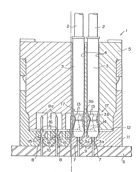
Referring to Fig. 2, a first embodiment of the
invention is shown and generally designated by the
reference numeral 1. The right half of the figure shows
those positions where coaxial pins 3 and signal pins 7
are inserted while the left half shows those positions
where~ground pins 8 are inserted.
The connector 1 comprises a coaxial pin housing 5
provided wlth a number oE deep bores 4. The pins 3
connected to respective coaxial cables 2 are inserted
into the respective bores 4 of~the housing 5. A number
of slgnal plns 7 and ground pins 8 are implanted in and
lS studd~ed on a substrate 6. The signal pins 7 engage with
the~respective plns 3. A ground pin housing ll is formed
with agroup of bores 9 and another group of bores 10 which
recelve the~ pins 7 and the~plns 8, respectlvely. A slngle
; thin plate of metal 12 is held between the houslngs 5 and~
11 and extends substantially perpendicular to the directlon
of insertlon of the pins 3, 7 and 8.
The plate 12 is cut and raised to form resilient
pieces or arms 13 at~those positions of the plate 12 where
the pins~3 inserted in the bores 4 from above intersect
the plate 12. As shown in the figure, the arms 13 extend
in the opposite direction to the direction in whlch the
:~
: : :
. ,.~ ..
~29~
- 6 -
pins 3 are inserted into the bores 4. Each of the pins 3
is formed with circumferential recesses 3b on its outer
periphery. When the pins 3 are received in the boxes 4,
they are individually resiliently retained by the arms 13.
The plate 12 are also formed with openings 14 in the
vicinity of the arms 13 so that the pins 3 are retained
with their tips 3a penetrating the plate 12 through those
openings 14. In this manner, coaxial pin contacts 17 are
formed in one-to-one correspondence with the pins 3.
The diameter of each of the bores 4 is small enough
to allow the pln 3 to be inserted smoothly but closely.
~As shown in the figure, the depth of each of the bores 4
is about four times greater than the height of each of
the arms 13. Such a conflguration causes each of the
pins 3 to be lnserted into between associated ones of the
arms 13 perpendicularly from above as viewed in the figure.
In other words, it prevents the pln 3 from being inserted
; wlth the pln 3 incllned or shifted to the side. As a
result, the arms 13 are safeguarded~against damage in the
event of lnsertion of the~plns 3. When the pins 3 are
inserted into the bores 4,~the pins 3 are brought into
positive contact~with the arms 13 at their outer periphery
while theipins 3 are surely retained by the~arms 13.
The p~ins 7 are inserted lnto the plns 3, whlch are
~received in the~openings 14 and~retained by the arms 13,
through the bores 9 from the tips 3a of the pins 3. This
:
:
.
~ ~ :
:: : :
.,~ .
. ' .
~: ~
Z527
-- 7
provides electrical connection between the signal lines
of the cables 2 and the pins 7.
The pins 8 are inserted into the bores 10
simultaneously with the insertion of the pins 7 into
the bores 9. The plate 12 is cut and raised at those
positions of the plate 12 where the pins 8 penetrate so
as to form resilient arms 15. The arms 15 extend in the
opposite direction to the direction of insertion of the
pins 8. Each of the pins 8 is resiliently retained by
associated ones of the arms 15 to form ground pin contacts
18. In this instance, the tips 8a of the pins 8 penetrate
openings 16 which are defined between the arms 15.
A prerequisite wlth the plate 12 is that the arms 13
and 15 be capable of retaiDing the pins with a sufficient
degree of~resilience and have a sufficient electrical-
conductivity with respect to high frequencies. To meet
this prerequisite, the plate 12 may be implemented by
a pIate of stainless steel plated with gold by way of
example.
As shown in Fig. 3, the contacts 17 and 18 are
located in close proximity to each other so that the
outer surfaces of the pins 3 and those of the ground
pins 8 are electrica]ly interconnected at the shortest
: : :
distance.
In the embodiment, the pins 3a are retained with
their tips 3a penetrating downward the openings 14 of
';~`'`'` ~'
~,:
~'
`~` 12925Z7
-- 8
the plate 12. Alternatively, an arrangement may be madesuch that the pins 7 penetrate the plate 12 upward through
the openings 14 into the pins 3 whose tips 3a are located
above the openings 14. Likewise, the ground pins 8 may
be reduced in length such that their tips 8a are positioned
below the plate 12, in which case the openings 16 are
omissible. Further, the arms 13 and 15 may be raised to
extend in the opposite direction to the direction as shown
in Fig. 2, that is, such that the arms 13 extend in the
same direction as the insertion direction of the pins 3
and the arms 15 extend in the same direction as the
lnSertlon directlon of the plns 8. If desired, the arms
13 and 15 may even be so formed as to extend in the same
direction. In these modiflcations, the configurations
of the two housings 5 and ll, the configurations and
lengths of the respective plns~shoùld be changed in
matching relation to the direction in which the arms 13
` ; and I5 extend. ~ ~ ~
Referring to~Flg.~4, a~general construction of the
connector~l in accordance wlth the present inventlon is
shown~in~a perspective view with the bores 4~ facing upward.
In the~figure, dash-and-dot lines~show that the bores 4
having the~same conflguration~are positioned in arrays.
Coaxial pins are inserted from above into the bores 4
25 ` while, at the same time, the same number of si~nal pins
:
~ ~ ~and ground pins as the coaxial pins are inserted from
:
:: :: ~ : ~: : : : : : :: : :
:
, ' - '
`` `~ lZ~S~7
. g
below into the connector 1, whereby electrical connection
is established as described earlier with reference to
Figs. 2 and 3.
In the specific construction shown in Fig. 4, the
connector l is divided into four blocks I, II, III and IV.
This is to prevent, for example, the coaxial pins from
failing to be inserted between their associated resilient
arma 13 due to errors particular to various kinds of
mac ~ such as forming the housings 5 and 11 and cutting
and raising the plate 12. If the connector 1 is not
` divlded lnto blocks and the plate 12 is implemented by a
single elongate plate, those errors would accumulate to
bring about the above-described insertion failure in a
part of the connector l. In the first embodiment, the
connector l is made up of a plurality of blocks each
~: :
including one short metal plate 12. Dividing the connector
into four blocks as shown and described is only illustrative.
`~ ` The gist is that one block be shorter than a particular
length whlch is detérmlned on the basis of the above-
described errors, a mounting a~ccuracy required and so on.
Referring to Fig. 5, a second embodiment of the
:: : : `
invention is shown which comprises a thin metal plate 112
in place of the thin metal plate 12~of Figs. 2 and 3. As
shown,~the plate 112 is cut and raised to form resilient
arms 113 at its positions for receiving the coaxial pins
3 (Flg. 2). ~A coaxial pin contact 117 is provided for
~: :
. .
, ' ~'
:
.; ' .,.
lZ9Z527
-- 10 ~
interconnecting any of the pins 3 and its associated
signal pin 7 (Fig. 2~ through an opening 114 which is
formed between the arms 113. The plate 112 is also cut
and raised to form another group of resilient arms 115
at its positions for receiving the pins 8 (Fig. 2).
A ground pin contact 118 is provided in which any of
the pins 8 is inserted through an opening 116 of the
plate 112.
In the second embodiment, upper portions of the
resilient arms 113 are further cut and raised to form
pawls 113a. In this configuration, when any of the
pins 3 is inserted into the opening 114, the pawls 113a
~; ~ of the arms 113 snap into the recesses 3b of the pin 3
; and in~the resultlng position prevent the pin 3 from
sllpplng out of~the connector l except when the pin 3
is~intentionally pulled~with~an~extraordinary force.
In~this~manner,~the~pawls 113a help their associated
reslllent~arms 113 surely retain the pin 3 within the
connector l.
2Q~ While~this inventi~on~has~been described in conjunction
wlth~the~preferred embodiments thereof,~it~will now
readi~ly~be~ possible~those~skilled in the~ art to~put thls
nvention into practice in various other manners.
:~ ~` : :
'
. ., ", . .