Note: Descriptions are shown in the official language in which they were submitted.
PRESERVATION OF SURFACE FEATURES
ON SEMICONDUCTOR SURFACES
sackground of the Invention
This invention relates to devices havi ~
surEace features on Group III-V compound semiconductors
and, more particularly, to preserving the integrity of
such features when they are heated.
Surface features on semiconductors (and other
materials) are used to affect the electrical, acoustical
10 or optical properties of devices incorporating the
~emiconductor. Optical gratings, for example, are an
array of parallel grooves formed on the surface of a
semiconductor to reflect or filter light of
predetermined wavelengths. In one specific application,
~ distributed feedback (~B) Group III-V compound
semiconductor laser, an optical grating serves as a
filter which allows the laser to operate in only a
sinqle longitudinal mode (i.e., at a single f~equency).
To this end, the amplitude and periodicity of the
grating are critical. The grating in such lasers is
typically formed on the surface of a substrate or
epitaxial layer and is then subjected to relatively high
temperatures during subsequent growth of epitaxial
layers over the grating. The effect of high
~5 temperatures during epitaxial growth is to deteriorate
the grating shape ~i.e., amplitude, spacing) which of
course degrades the single-frequency performance of the
laser.
Although grating degradation has been couched
in terms of subjecting the grating to the temperatures
of epitaxial growth, even if such growth were not
employed in a particular device application (e.g., in
the case of a grating on the top surface of an optical
3~
waveguide layer), other hlgh temperature processing steps
might also adversely affect the grating's characteristics.
The present invention avoids this problem.
Summary of the Invention
The integrity of surface structural features, such
as optical gratings, on Group III-V compound semiconductors is
preserved during heating by a thin coating which contains a
transition metal. Sub-monolayer coverage has been found
effective with coatings containing Os, Ru or Rh. Where liquid
phase epitaxial (LPE) growth over the grating is employed,
coatings containing Ru or Rh are presently preferred.
In accordance with one aspect of the invention there
is ~rovided a method of manufacturing a device which includes
protecting a surface feature on a Group III-V compound
semiconductor from substantial deterioration during heat
treatment by applying to at least the feature a thin
protective coating containing a transition metal prior to the
treatment.
In accordance with another aspect of the invention
there is provided in a method of fabricating a laser, the
steps comprising providing an InP body, forming an optical
grating on the body, forming a thin protective coating
containing a transition metal on the grating, and epitaxially
growing on the grating a heterostructure which includes a
plurality of layers of InP and/or InGaAsP.
In accordance with yet another aspect of the
invention there is provided a DCPBH laser comprising a Group
III-V compound semiconductor body having a major surface, an
optical grating on said major surface, a thin protective
coating on said grating, said coating including a transition
metal, a base semiconductor heterostructure formed on said
grating and including a pair of channels and a mesa
therebetween, said mesa including a Group III-V compound
semiconductor active layer, an embedding semiconductor
structure which fills said channels and covers said mesa, said
structure being effective to direct the primary flow of
current through said mesa during operation of said laser, and
2 a ~L~9;~S~8
means forming electrical contact to said laser.
Brief Description of the Drawi~
FIG. 1 is a schematic of a DCPBH laser in accordance
with one embodiment of my invention; and
FIG. 2 is a schematic of a portion of the laser of
FIG. 1 prior to LPE regrowth and metalization to show the
grating on the substrate.
Detailed Description
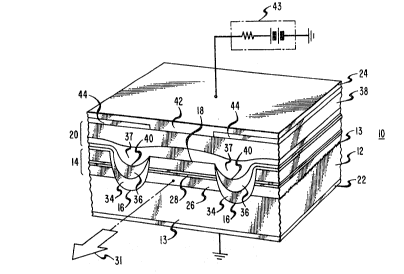
Turning now to FIG. 1, there is shown a double
channel planar buried heterostructure (DCPBH) laser lO
comprising an InP body (e.g., an n-InP (100)-oriented
substrate 12) on which a grating 13 is formed so as to effect
single frequency operation. Alternatively, an n-InP buffer
layer may be grown on the substrate with the grating formed on
the buffer layer. The grating lines run parallel to the (011)
direction, which is also parallel to the laser mirror facets,
and may be formed by any means well known in the art. A
suitable technique includes holographic exposure of
photoresist on the substrate and chemical etching of the
substrate material. A multilayer base structure 14 is grown
by LPE on the grating and a pair of channels 16 are etched in
the base structure 14 so as to form a mesa 18 which includes
the active, light-emitting layer 28 of the laser. Thereafter,
an embedding structure 20 is
_ 3 _ ~29Z5~8
structure 20 is epitaxially grown in the channels and
over the mesa. Metal contacts 22 and 24 are then formed
on the substrate 12 and on the top of the embedding
structure 20, respectively.
The base structure ~IG. 2) illustratively
includes an n-InGaAsP waveguide layer 26 on the
substrate, an undoped (or unintentionally do?ed) InGaAsP
active layer 28, an optional anti-meltback InGaAsP (~ ~
1.3 ,um) layer 30 (used in longer wavelength lasers such
as those operating at ~ ~ 1.5 ~m), and a p-InP cladding
layer 32. The actual wavelength of operation depends on
the composition of active layer 28 and ls generally in
the range of about 1.1 ~m to 1.6 ,um (typical about
1.3 ,um or 1.5,um depending often on the type of optical
- 15 fiber used in conjunction with the laser)~ The bandgap
of the waveguide layer 26 is greater than that of the
active layer 28 so that light generated in the active
layer is coupled to and guided in layer 26.
Alternatively, the anti-meltback layer 30 may also serve
as a waveguide layer.
In one embodiment, the embedding structure 20
(FIG. 1) includes p-InP layers 34 and n-InP layers 36
which confine current to flow predominantly through the
mesa 18, a p-InP layer 37 which covers the channels and
the mesa 18, and a p-InGaAsP or p-InGaAs cap or
contact-facilitating layer 38. The interfaces between
p-type layers 37 and n-type layers 36 form p-n
junctions 40 which are reverse biased when the device is
forward biased during operation. Junctions 40 thus
block substantial current flow around the mesa and cause
most of the pump current from source 43 to flow through
the mesa and hence through the active layer 28. Light
generated in the active layer 28 is coupled into the
wider bandgap, waveguide layer 26 and is emitted as a
beam in the general direction of arrow 31.
- 4 - ~ S~
An alternative to the reverse-biased
junctions 40, which block current flow imper~ectly a
at times inadequately in high speed (bit rate)
applications, is to use metal-organic chemical vapor
deposition (MOCVD) to regrow semi-insulatiny Fe~doped
InP in the channels as discussed in co-pending
application Serial No. 621,071 filed
on June 15, 198~ (Johnston-Long-Wilt 19-3-3).
In the case of either embedding structure, it
may be desirable to configure the top contact 24 in the
form of a stripe to further constrain current to flow
predominantly through the mesa 18. As shown in FIG. l,
the stripe 42 may be delineated by suitable masking via
dielectric layers 44.
In accordance with one embodiment of my
invention, after the grating is formed and before LPE
growth of the base structure thereon, a thin coating
containing a transition metal is formed on the grating.
Sub-monolayers of Ru or Rh are effective to protect the
shape of the grating from significant degradation during
LPE growth processes which typically involve
temperatures in the range of about 550C to 700C.
Other transition metal coatings, such as those
containing Os, also protect the grating from the adverse
effects of high temperatures, but may not have wetting
characteristics as desirable as the Rh or Ru-containing
coatings for LPE growth. Thus, Os-containing coatings
may be used on, for example, the top surface of optical
waveguides where LPE growth thereon is not an issue but
where heating may still cause a grating integrity
problem. Such heating could arise, for example, where
the waveguide is part of an integrated optical circuit
which includes a device that itsel~ involves high
temperature processing (e.g., LPE growth or contact
alloying).
, .
5~1~
- 5 -
A novel process by which the protective
coating can be formed on the grating or other surface
structural feature is now described. An aqueous
solution comprising a transition metal salt dissolved in
an acid is applied to the grating to form the coating
thereon In one embodiment the salts are trichlorides
of os, Rh or Ru and the acid is HCl. However, other
transition metal salts in conjunction with other acids
are expecte~ to be suitable. Moreover, although certain
embodiments and examples of my invention are described
in the context of LPE, t~ transition metal coating can
also be used in conjunction with other epitaxial
techniques such as vapor phase epltaxy. In each case,
after the coating is formed, the grating or other
structural surface feature may be subjected to heating
without experiencing significant degradation.
The lnvention also can be also be employed to
protect structural features on other Group III-V
compounds such as InGaAsP.
The following examples are described by way of
illustration only and, unless otherwise stated, the
specification of various parameters is not intended to
limit the scope of the invention.
Example I
In this example, we used a holograph and
chemical etching to produce second order feedback
gratings having grooves parallel to the (OlI) crystal
direction of InP wafers (substrates). The dimensions of
the grating were: spacing about 0.464,um; height about
0.2 ,um. The nomi ~l surface orientation of the InP was
(lO0) with an accuracy of 0.2 . All wafers were n-type
material with doping ranging from about 3X10l7 to
3Xl0l8/cm3. Wafers fabricated by both a vertical
gradient freeze (Ga~ t) process and a liquid
encapsulated Czochralski (LEC) process were used~ No
dependence upon substrate orientation, doping, or growth
method was observed.
- 6 - ~Z9~
All wafers were cleaned by ~irst boiling in
chloroform, acetone, and methanol to remove organic
contaminants and then etching in 10:1:1 (H2SO4:H2O2:H2O)
at room temperature for one minute~ The wafer was then
thoroughly rinsed in deionized water and dried under a
stream of nitrogen gas. A protective coating was formed
on the grating by application of a few drops of an
aqueous solution of a transition metal salt to fully
cover the wafer surface. After about 5 seconds, this
solution was removed by a thorough deionized water
rinse. The wafer was then blown dry in a stream of
filtered nitrogen, and transferred into an epitaxial
growth reactor for either heat treatment or LPE growth.
Solutions of salts of the transition metal
ions Ru, Rh, and Os were used. Ru and Rh were contained
in 0.1 M solutions of their trichlorides in 0.2 M HCl.
Os was contained in a 0.05 M solution of its trichloride
in 0.2 M HCl.
;In this example, the wafer with its etched
grating and protective coating were subjected to a heat
treatment in an LPE system. The heat treatment cycle,
which simulated the growth of a 1.55,um planar laser
structure for use in making DFB-DCPBH lasers, involved
heating the wafer to 600C for 90 minutes (corresponding
to the conditions which would be used to homogenize the
growth melts) followed by ramping to 580C over a period
of 30 minu~es (corresponding to conditions which would
;be used to grow the double heterostructure). Duri~
heating, the wafer was protected from thermal
degradation by an overpressure of phosphorus supplied
from a solution of InP, Sn, and InAs, in a chamber of
the type described by P. 8esomi et al in
U.S. Patent No. 4,48~,423 issued on November 13, lY~.
As a result of the protective coating,
essentially no deformation of the grating etched surface
through the heat treatment occurred, while a control
sample with a grating having no coating exhibited
.
- 7 ~ Z S ~
.. ~
significant degradation. Similar results were o~tained
for gratings on wafers coated from solutions of Ru, Rh
or Os.
Examp_ II_
The procedures of Example I were repeated to
form a Ru-containing protective coating on the grating
etched in the InP wafers, but this time the base
structure 14 of a DCPBH laser was grown by LPE over the
grating-etched wafers. The base structure, as shown in
FIG. 2, comprised a 0.20 ~m thick (average thickness)
InGaAsP (~ - 1.3 ~m) wavequide layer 26 doped n-type
with Sn to about 7X10¹⁷/cm3, a 0.20,um thick InGaAsP
(~ _ 1.55,um) active layer 28 (unintentionally doped),
and a 0.68 ~m thick InP cladding layer 32 doped p-type
with Zn to about lX1018/cm3. In this particular example,
the p-type anti-meltback layer was not grown, although
our later experience found it to be desirable. After
suitable masking, channels 16 were etched to form
mesa 18 which was about O.9,um wide at the top and 2.6
,um deep at the bottom of the channels. LPE regrowth was
then used to form the embedding structure 20 which
included 0.6 ,um thick InP layers 34 doped p-type with Zn
to about lxlO18/cm3, 0.5 ,um thick InP layers 36 doped
n-type with Sn to about lX1018/cm3, a 2.6 ,um thick InP
layer 37 doped p-type with Zn to about lX1018/cm3, and a
1.0 ~m thick InGaAs
1.65 ~m) contact-facilitating layer 38 doped p-type
with Zn to about ~X1018/cm3. The thicknesses of the
layers of the embedding structure were measured in the
planar region outside the channels. Electrical contacts
22 and 24 were then deposited as described earlier, and
the wafers were cleaved into individual DFB-DCPBH laser
chips.
X-ray photoelectron spectroscopy (XPS) showed
that the content of the coating had about 1.3 atomic
percent Ru, and the coating's coverage of the wafer
surface was about 0.06 monolayers or less. Less than
_ - 8 ~ ~?~9 Z S'~
complete coverage of the grating surface may be
important to LPE growth which generally requires a
significant portion of the semiconductor to be exposed
in order to obtain adequate wetting of the LPE melt.
The threshold currents of the lasers
fabricated from these wafers were essentially identical
to those fabricated without the Ru coating, which
indicates that the small amount of transition metal
present in the structure does not degrade the material
10 .or device quality.
Example III
The procedures of Example II were repeated to
the exten-t that the base structure was grown, but in
this case a Rh-containing protective coating was formed
on the grating~ XPS showed that the content of the
coating had about 0.5 atomic percent Rh, and the
coating's coverage of the wafer surface was about 0.06
monolayers or less.
The base structures were optically pumped with
a Nd:YAG laser (1.06,um) so that the active layer 28
lased in a single longitudinal mode. This experiment
demonstrated that the base structure was suitable for
incorporation into a single-frequency laser.
Example IV
~5 The procedures of Example II were repeated in
an attempt to grow a base structure, but in this case an
Os-containing protective coating was formed on the
grating. XPS showed that the content of the coating had
about 3.0 atomic percent Os and the coating's coverage
of the wafer surface was about 0.15 monolayers.
With the Os coating, the grating was preserved
well in heat treatment, but the wafer surface would no
longer adequately wet with the epitaxial growth melts.
The resulting wafer was covered uniformly with islands
of epitaxial growth, typically 1 ~m in size, suggesting
that too much coverage by the Os coating layer either
reduces the density of growth nucleation centers or
9 ~ 5~8
impedes the coalescence of nucleated islands dur ing
growth ~