Note: Descriptions are shown in the official language in which they were submitted.
~ 2~ 7 RCA 84,983
VIDEO DISPLAY DRIVER_APP RATUS
This invention concerns a display driver
amplifier and output signal coupling network ~or providing
a high level video output signal to an image display
device. In particular, this invention concerns such
apparatus with increased high frequency response.
In a television receiver a video output display
driver amplifier provides a high level video output signal
to an image display device such as a kinescope. The video
output signal is conveyed via an output signal coupling
path to a signal input electrode of the kinescope, e.g., a
cathode electrode. The kinescope signal input electrode
can exhibit a capacitance which is large enough ~o impair
the high frequency response of the video signal developed
at the output of the driver amplifier. Thus it is
desirable to reduce the effect of the kinescope capacitance
upon the driver amplifier output signal, thereby preventing
degraded video signal high frequency response and degraded
image resolution.
This objective is achieved by means of a video
output signal coupling path in accordance with the
principles of the present invention. In an illustrated
preferred embodiment of the invention, the video output
signal coupling path conveys a video signal from the output
of the display driver amplifier to the input of the
kinescope by means of first and second cascaded emitter
follower transistors of opposite conductivity type. The
follower transistors respectively isolate the display
driver output from the kinescope capacitance in the
presence of positive and negative video signal amplitude
excursions. First and second unilateral current conducting
devices, such as diodes, are respectively connected across
the base-emitter junctions of each transistor and are poled
for forward current conduction in a direction opposite to
that of the associated base-emitter junction.
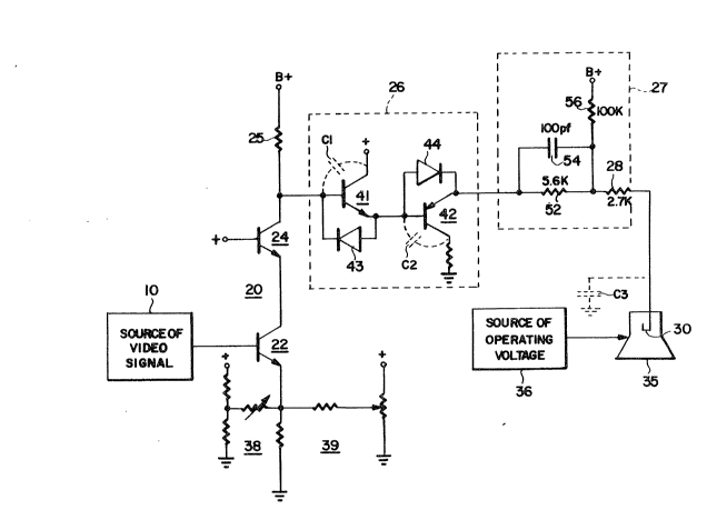
The sole figure of the drawing illustrates a
portion of a television receiver including a video output
s~
`- -2- RCA 84,983
signal coupling network in accordance with the principles
of the present invention.
A low level video signal from a source 10 is
applied to a kinescope driver stage 20 including an input
low voltage common emitter amplifier transistor 22 arranged
in a cascode video amplifier configuration with an output
high voltage common base amplifier transistor 24. A hi~h
level amplified video signal with a magnitude suitable for
driving a signal input cathode electrode 30 of a kinescope
35 is developed in a collector output circuit of transistor
24, including a load resistor 25 coupled to a high
operating voltage B+ (e.g., +230 volts). An amplified
video output signal developed across resistor 25 is coupled
to cathode electrode 30 via a network 26, a frequ~ency
compensated drive level compensation network 27 in
accordance with the principles of the present invention,
and a kinescope arc current limiting resistor 28, commonly
referred to as a "flashover" resistor, operatively
associated with network 27. The signal gain and the DC
bias of driver stage 20 are respectively adjusted by means
of a variable resistor 38 and a potentiometer 39 in the
emitter circuit of transistor 22. Operating voltages for
kinescope 35 are provided by a source 36.
A capacitance C3 represents parasitic kinescope
and wiring capacitance associated with kinescope cathode
electrode 30. The value of this capacitance is
approximately 9 picofarads and can result in significant
high frequency degradation if it is permitted to influence
the video signal developed across resistor 25 in the output
circuit of transistor 24. Network 26 is arranged to reduce
or eliminate such high frequency degradation by decoupling
such capacitance from the collector output circuit of
transistor 24.
Coupling network 26 includes an NPN emitter
follower transistor 41 with a low impedance emitter output
electrode and a PNP emitter follower transistor 42 with a
low impedance emitter output electrode arranged in cascade
in the output signal path from the collector output circuit
~ ''325is~7
-3- RCA 84, 983
of transistor 24 to kinescope 30. Parasitic collector-base
capacitances Cl and C2, e.g., 2 picofarads, are
respectively associated with transistors 41 and 42 and
include stray wiring and layout capacitances. Diodes 43
and 44 are coupled across the base-emitter junctions of
transistors 41 and 42, respectively, and are poled for
forwaxd current conduction in a direction opposite to the
forward current conduction direction of the associated
base-emitter junction.
A rapid positive amplitude transition, which
contains significant high frequency image detail
information, is conveyed to kinescope 35 via conductive
transistor 41 and conductive diode 44. Diode 43 and
transistor 42 are reverse biased (nonconductive)~at this
time.
In the case of a rapid positive-going video
signal amplitude transition at the collector output of
transistor 24, the capacitance presented to the collector
output of transistor 24 iS substantially equal to
C1 + C2/~41 + C3/~41 (1)
where capacitances Cl, C2 and C3 are as discussed above and
~41 is the forward current gain (Beta) of transistor 41,
typically lO0 minimum. Thus at the collector of driver
transistor 24 the value of kinescope capacitance C3 is
greatly reduced by the Beta (~) of transistor 41, and the
value of relatively small capacitance C2 is reduced further
by the Beta of transistor 41. Resistor 28 assists to
isolate the kinescope capacitance from the output circuit
of driver transistor 24, ~ut the effect of such action is
much less than that produced by network 26.
Rapid negative amplitude transitions, which also
contain significant high frequency image detail
information, are conveyed to kinescope 35 via conductive
diode 43 and transistor 42. Transistor 41 and diode 44 are
reverse biased at this time. For rapid negative-going video
signal amplitude transitions at the collector output of
transistor 24, the capacitance presented to the collector
output of transistor 24 is substantially equal to
557
-4- RCA 84, 983
Cl ~ C2 + C3/,B42 ( 2 )
where ~42 is the forward current gain of transistor 42,
typically 100 minimum. Thus the relatively large value of
kinescope capacitance C3 is greatly reduced by the Beta o~
transistor 42 at the collector of driver transistor 24.
A relatively large bypass capacitor 54 ~hunting a
resistor 52 in network 27, as will be discussed
subsequently, has a negligible effect upon the value of
capacitance given by expressions (1) and (2) above since
the value of capacitance presented to the emitter of
transistor 42 is dominated by capacitance C3.
Note that the base-emitter junctions of
transistors 41 and 42 are not bypassed by capacitors. Such
bypassing of one or both of these transistors would defeat
the purpose of isolating the output circuit of transistor
24 from capacitances such as kinescope capacitance c3 and
capacitor 54 in this example, in the presence of positive
or negative signal amplitude transients or both.
A display driver stage including coupling network
26 has been found to exhibit a significant improvement in
high frequency response due to decoupling kinescope
capacitance C3 from the output circuit of transistor 24, as
well as a substantially symmetrical positive and negative
transient response. In the latter regard it is noted that
expressions (l) and (2) above contain different values of
capacitance for positive and negative amplitude transients.
The difference is small, however, and transistor 24 can
more easily drive a capacitive load when exhibiting
increasing current conduction and an associated decreasing
collector impedance in response to negative signal
amplitude excursions, compared to driving a capacitance
when exhibiting decreasing conduction and increasing
collector impedance in response to positive amplitude
excursions.
Network 26 can assume configurations other than
that shown. For example, when a PNP transistor is employed
for driver 24 the positions of transistors 41 and 42 with
associated diodes 43 and 44 should be interchanged.
.. . .
~Z~57
-5- RCA 84,983
With the disclosed arrangement the value of
collector load resistor 25 can be lowered in value because
the kinescope does not directly load the collector circuit
of transistor 24, i.e., the collector circuit is buffered
via follower transistors 41 and 42. A lower value of
collector load resistance advantageously enhances high
frequency response since a smaller resistance value
produces less of a lowpass filtering effect together with
parasitic collector circuit capacitances.
Network 27 includes a series coupling resistor 52
and a frequency compensation capacitor 54 arranged in
parallel as shown, together with flashover resistor 28. A
resistor 56 is coupled between an operating voltage (B+)
and a point in the signal path to which capacitor~ 54 is
coupled.
Network 27 compensates for the tendency of an
image display device such as kinescope 35 to "bloom", or
conduct excessive current, when driven by a large magnitude
video signal from a low impedance source such as the
emitter output of PNP follower transistor 42. To this end
resistor 28 and resistor 52 do not develop a significant
voltage drop for kinescope current conduction in response
to a video signal of low to moderate magnitude. However,
resistors 52 and 28 develop a significant voltage drop for
kinescope current conduction in response to a large
magnitude video signal, e.g., representative of a bright
image. This voltage drop reduces the signal drive to
kinescope cathode electrode 30, thereby reducing or
eliminating the likelihood that the kinescope will "bloom"
under large signal conditions. The values of resistors 52
and 28 and capacitor 54 are chosen to yïeld a desired
display drive impedance, particularly at low through middle
video signal drive levels which determine image brightness
and intensity, so as to maintain kinescope current
conduction in accordance with a gamma correction function
as is known. The values of resistors 52 and 28 can be
tailored to provide a desired amount of gamma correction
557
-6- RCA 84,983
depending on the type of kinescope and its current
conduction characteristics.
Capacitor 54 is a high frequency bypass element
to compensate for a high frequency loss associated with a
lowpass filtering effect produced by the coaction of
kinescope capacitance C3 with resistors 28 and 52. The
high frequency compensation provided by network 27 begins
at approximately 500 KHz, which is well within the DC to
4.2 MHz video signal band according to NTSC standards. The
amount of high frequency compensation, including high
frequency boost, is a function of the values of capacitor
54, resistors 52 and 28, capacitance C3 and the impedance
of kinescope cathode 30. The impedance of cathode 30 is a
function of the current conduction level of catho~de 30. In
this example, more high frequency compensation is provided
at higher cathode current levels.
Capacitor 54 could be coupled across resistor 28
instead of across resistor 28 as illustrated. However, it
is preferred that the non-bypassed resistor be located as
close to the kinescope as possible to minimize the damage
to circuit boards and associated circuit elements due to
kinescope arcing. Placing bypass capacitor 54 across both
resistors 52 and 28 would defeat the intended arc current
protection since such a capacitor coupling would provide an
arc current path circumventing the current limiting effect
of resistor 28 in this case.
Resistor 56 provides a bias for kinescope cathode
30 to assure that the kinescope is blanked during retrace
intervals. Resistor 56 also assists capacitor 54 in
providing the desired high frequency compensation at
various signal drive levels. Specifically, resistor 56
helps to stabilize the effective impedance presented to the
network including resistor 52 and capacitor 54, in the
presence of kinescope impedance variations associated with
changes in the level of kinescope current conduction due to
changes in the drive signal level.