Note: Descriptions are shown in the official language in which they were submitted.
i2~Z770
Description
Apparatus and Method
For Controlling A
Force Commutated Inverter
Technical Field
This invention relates to force commutated
inverters and more particularly to a method for
generating gating signals for the switches in the
output stage of such an inverter in order to produce a
variable frequency pulse-width modulated (PWM) output
waveform with the appropriate percent fundamental
voltage. In the case of an inverter connected to a
utility line the correct phase relationship to the
line is maintained.
Background Art
Control of an independent inverter's output
voltage is required or, in the case of an inverter
operating in parallel with a grid, control of the
output phase and voltage is reauired to achieve,
respectively, a desired real and reactive power
operating point. Such an inverter controller may be
thought of, in simplified form, as being responsive to
a voltage command or to separate, externally supplied
real and reactive power command signal levels which
may, of course, change depending on operating
conditions.
Such a control (for the case of an inverter
operating on a grid) is described in U. S. Patent No.
4,251,735 entitled DUAL SPEED CO~TROL CIRCUIT FOR
C-1517
~29Z770
POWER FLOW THROUGH AN INVERTER, issued to Allen K.
Coleman on February 17, 1981 and assigned to the
assignee of this patent. There, a control circuit
varies the real power component and the reactive power
component of the electrical energy flowing between a
DC source and a utility power grid. Independent
control of the magnitude of both the real and reactive
components is disclosed in both U. S. Patent No.
4,251,735 and in another patent, U. S. Patent No.
4,2Sl,736, issued to the same inventor on the same
date and also assigned to the assignee of this patent.
Thus, it is now known that real and reactive power
components may be varied substantially independently
using separate reactive and real power command signals
input to a controller.
In addition, U. S. Patent No. 4,251,735 discloses
a look-up table for storing pulse width modulated
waveform patterns for use in a switching waveform
generator. The switching waveform generator responds
to a voltage controller to select one of the stored
switching waveform patterns for switching the inverter
output stage main switching elements, normally
thyristors or other solid-state switches, such that
the output voltage waveform has a certain effective
fundamental voltage. This controls the reactive power
component. Also, the particular pattern is phase
offset in proportion to the signal presented to the
switching waveform generator from a phase controller
to the switching waveform generator in order to
control the real power component. Coleman discloses
one embodiment of a switching waveform generator which
~Z~?Z770
includes a look-up table responsive to an eight line
digital data bus from the voltage controller. The
look-up table stores, in digital format, the
predetermined width of various notches in the
switching pattern waveform at which the thyristors of
each bridge in the output stage of the inverter should
be transitioned to create a voltage output waveform
having the particular desired effective voltage
magnitude. As recorded information is addressed by
the eight bit input words, an output is presented to a
digital comparator which is also responsive to a phase
shift signal. The comparator digitally combines the
signal from the look-up table indicating the pulse
width modulation information with the phase
displacement information and provides a switching
waveform for use by the output stage switches of the
inverter. In accordance with this switching waveform
pattern, the individual switching elements in the
inverter are transitioned between the conducting and
the nonconducting states and the power output has the
desired real and reactive components.
Fig. 4 of U. S. Patent No. 4,251,735 illustrates
an inverter output waveform having a selected number
of transitions per cycle. There, a technique known as
"end notching" is shown whereby the end of each half
cycle is pulse width varied. This causes a change in
the effective magnitude of the fundamental component
out of the inverter. A desired fundamental component
compatible with that of the power grid is often used
by those skilled in the art to describe the voltage
magnitude provided by the inverter output. As
lZ92770
mentioned, the magnitude of the percent fundamental
component controls the reactive power component and
is directly proportional to the reactive power
command signal magnitude. A feature of the Coleman
invention was that the switching waveform generator
can linearize voltage controller feedback so that the
effective voltage out of the inverter decreases as
the width of the notch increases in a linear manner.
This is done by means of a multiplier in a feedback
loop of the voltage controller.
In the prior art, as described above, the
methods used to generate varying PWM waveforms used
continuous modification of a fixed switching fre-
quency pattern over a modulation range. With this
method, it is possible to optimize harmonic cancel-
lation at only one reactive power operating point.
Disclosure of The Invention
The object of the present invention is to
provide a method which provides the designer with the
flexibility required to select advantageous harmonic
cancellation at a plurality of fundamental voltages.
In accordance with the invention there is
provided a method for controlling the conduction
states of an inverter's output stage switches for
controlling the voltage output of the inverter
according to the magnitude of a voltage command
signal. The method includes the steps of stori,ng a
plurality of digital signal groups, each group having
a selected number of timing count words, each word
indicative of a particular time interval between
successive potential changes in the conduction states
of the inverter's output stage switches. Each group
also has a polarity word indicative of which of said
successive potential changes will actually result in
a change in the conduction states of the inverter's
lZ92~'70
- 4a -
output stage switches. The method also includes the
step of retrieving a stored signal group according to
the magnitude of the voltage command signal, and
successively counting to the magnitudes of each of
the timing word counts in the retrieved group and, at
the end of each count, determining from the polarity
word whether a conduction state change is indicated
and providing a switch signal for each such indica-
tion.
The invention also relates to a method for
controlling the conduction states of an inverter's
output stage switches for controlling the real and
reactive power output components of the inverter
according to the respective magnitudes of real and
reactive power command signals. The method includes
the steps of storing a plurality of sequences of
transition initiating signals for initiating transi-
tions in the states of the inverter output stage
switches. Each sequence effects a selected number of
inverter output current reversals. Each sequence is
related to a particular one of a plurality of groups
of stored sequences by having the same number of
transition initiating signals within its sequence as
every other sequence within the particular related
group. A reactive power command signal is responded
to by selecting a stored sequence and providing a
timed sequence of inverter output current reversals
which in turn effects the commanded reactive power
output component. A real power command signal is
responded to by time shifting the selected sequence
to effect the commanded real power output component.
~ he invention also relates to apparatus for
controlling the conduction states of an inverter's
output stage switches for controlling the voltage
output ~f the inverter according to the magnitude of
1~927~'0
- 4b -
a voltage command signal. The apparatus includes
memory means for stori.ng a plurality of digital
signal groups. Each group has a selected number of
timing count words, each word being indicative of a
particular time interval between successive possible
changes i.n the conduction states of the inverter's
output stage switches. Each group also has a polar-
ity word indicative of whether each of the successive
possible changes will actually result in a change in
the conduction states of the inverter's output stage
switches. A central processing means retrieves a
stored signal group according to the magnitude of the
voltage command signal for successively counting to
the magnitudes of each of the timing word counts in
the retrieved group. At the end of each word count,
it is determined from the pol.arity word whether a
conduction state change is indicated and a switch
signal is provi.ded for each such indication.
Also, in accordance with the invention, there
i.s provided apparatus for controlling the conduction
states of an inverter's output stage swi.tches for
control.ling the real and reactive power output
components of the inverter according to the respec-
tive magnitudes of real and reactive power command
signals. The apparatus includes memory means for
storing a plurality of sequences of transition
i.nitiating signals for i.nitiating transitions in the
states of the inverter output stage switches. Each
sequence effects a selected number of i.nverter output
current reversals, and each sequence is related to a
particular one of a plurality of groups of stored
sequences by having the same number of transiti.on
ini.ti.ating signals within its sequence as every other
sequence within the particular related group. Cen-
tral processing means are responsive to a reaetive
lZ9Z7'~0
power command signal for selecting a stored sequencefor providing a timed sequence of inverter output
current reversals for in turn providing the commanded
reactive power output component. The central pro-
cessing means is also responsive to a real powercommand signal for time shifting the selected se-
quence for providing the commanded real power output
component.
According to the present invention, there is
provided a method for varying both the number of
notches and their width, such that a plurality of
variable frequency "pulse width modulated" (PWM)
output waveform patterns are provided. Individual
patterns for every operating point are stored in a
memory. As mentioned, patterns may have different
numbers of notches, i.e., may be of different
"frequencies". Patterns may be grouped by
"frequency" and the separate patterns within a
125~Z~o
frequency group will have different pulse widths.
With this method, different frequency patterns can be
designed for selection during operation over the
entire modulation range for more advantageous harmonic
cancellation.
In further accord with the present invention, for
the case of inverters used in parallel with other
energy sources, for lagging reactive power command
signals, a stored pattern having a high number of
transitions, or notches, i.e., a high "frequency," is
selected and, for leading reactive power command
signals, a low frequency pattern having a low number
of transitions or notches is selected. A similar
principle is used for the case of inverters used for
independently supplying a load, except that there is
only a voltage command. I.e., a high frquency is used
for lower voltage commands while a lower frequency is
used for higher voltage commands.
In still further accord with the present
invention, for the case of an inverter in parallel
with a utility grid, the notching of the various
stored patterns is generally such that for leading
reactive power command signals the pulse widths or
notch magnitudes tend to be smaller in most cases. In
some cases larger notches will exist for lower
commands but these will tend to be nearer to zero
crossover points. Similarly, for lagging reactive
power command signals the pulse widths or notch
magnitudes tend to become higher. In other words, the
portion of a positive half cvcle in which positive
current is flowing is greater for leading reactive
lZ~Z7'70
-- 6 --
power command signals and smaller for lagging reactive
power command signals. This is accomplished with
smaller notches for leading commands and larger
notches for lagging commands. For the case of an
inverter which independently supplies a load, a
similar principle applies except there is only a
voltage command signal, as described above.
With this method or apparatus, each waveform
pattern over the entire moduation range can be
carefully selected for the desired percent fundamental
by the designer for an advantageous harmonic
cancellation.
These and other objects, features and advantages
of the present invention will become more apparent in
light of the detailed description of an embodiment
thereof, as illustrated in the accompanying drawing.
Brief Description Of The Drawing
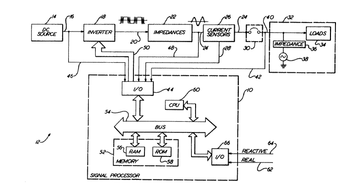
Fig. 1 is a simplified block diagram illustration
of a force commutated inverter controlled by a signal
processor controller, according to the present
invention;
Fig. 2 is a simplified illustration of the basic
principle involved in all inverters;
Fig. 3 is an illustration of the load current
flowing through the load resistor of Fig. 2;
Fig. 4A is a simplieied illustration of a full
wave three-phase inverter, which is shown delivering
alternating currant to a three phase load;
Fig. 4B is a simplified illustration of a
six-device inverter utilizing an isolating three-phase
transformer;
lZ9Z7 ~0
Fig. 5 is a simplified illustration of an
individual commutation circuit;
Fig. 6 is an illustration of a two-bridge
inverter which may employ one or more inverter
controllers according to the present invention;
Fig. 7 is an illustration of a possible waveform
pattern for initiating inverter output stage switch
transitions and also showing the relationship of the
transition initiating signals to the inverter output
current
Fig. 8 is an illustration of several waveforms
illustrating a transition initiating signal for a 540
hertz waveform pattern and the resulting output
currents;
Fig. 9 illustrates five pairs of transition
initiating signals, each pair representing the first
and last waveform from the five frequency groups of
Table I;
Fig. 10 is an illustration of a basic inverter
control, according to the present invention;
Fig. 11 is a data map for storing a one quarter
wave pattern:
Fig. 12 is an illustration of a line
synchronization and phase shift timing diagram for a
three-phase system;
Fig. 13 is a simplified flowchart illustration of
the logical steps executed by a signal processor in
order to provide the half wave sync pulses illustrated
in Fig. 12, according to the present invention;
lZ9Z7 ,0
-- 8 --
Fig. 14 is a simplified flowchart illustration of
a control flowchart for controlling the inverter
output stage switches, according to the present
invention; and
Fig. 15 is a simplified flowchart illustration of
the "GATES~ subroutine referred to in Fig. 14.
Best Mode ~or Carrying Out The Invention
Fig. 1 is an illustration of a controller 10,
according to the present invention, for controlling an
inverter system 12 which includes a DC source 14
supplying DC on a line 16 to a force commutated
inverter 18 which, in turn, provides a
quasi-squarewave output on a line 20 to a paralleling
impedance 22. A quasi-sinusoidal output waveform is
lS provided on a line 24 to a current sensor 26 which
provides an output signal on a line 28 indicative of
the magnitude of the current on line 24. The output
current continues on through the current sensor 26 on
line 24 to a circuit breaker 30 which may be opened or
closed in order to connect the outPut of the inverter
to a utility grid 32 which includes various loads 34,
an impedance 36 and a generalized source 38. The
voltage of the utility buss on a line 40 is sensed on
a line 42 and provided to an input/output (I/O) port
44 within the controller 10, which may be a signal
processor. Control of the breaker may be effected in
- the controller 10, or may be cffected elsewhere and is
not described herein as it is not relevant to the
invention. The I/O port 44 is also responsive to a
signal on a line 46 which senses the DC output voltage
lZ9Z7~0
from the DC source and to a signal on a line 48 which
senses the voltage and phase of the quasi-sinusoidal
waveform on the line 24. The output port 44 also
provides a plurality of transition initiating signals
on a line 50 for initiating transitions in the output
stage switches of the inverter 18. The disclosed
method and apparatus 10 for controlling the timing of
these signals 50 is the subject matter of the present
invention.
It will be understood that although the
illustration of Fig. 1 shows an inverter in parallel
with a utility grid, such that real and reactive power
levels are of concern, the principles taught herein
are equally applicable to the case of an inverter
acting as the sole source for a load in which case
voltage control alone is of concern. Although much of
the discussion contained herein is directed to the
case of an inverter supplying a grid, it should be
understood that the notching techniques and storage of
patterns described herein for controlling reactive
power are also applicable for simply controllinq
voltage for the case where a real power command signal
is absent, i.e., for independent inverter operation.
The signal processor 10 includes a memory 52
which communicates with a data and control buss 54.
The memory 52 may include random access memory 56
(RAM) and read only memory 58 (ROM). Of course, it
will be understood that the memory units may be
external to the signal processor. However, many
microcomputers now have PROMs internally. A central
processing unit 60 (CPU) also communicates with the
lZ.'3Z770
-- 10 --
data and control buss 54 and contains the necessary
hardware for executing program steps stored in ROM 58
and RAM 56. The signal processor 10 is also
responsive to a real power component command signal on
a line 62 and a reactive power component command
signal on a line 64 at an input/output port 66 (I/O).
These two signals may be thought of as externally
provided command signals which may be constant or of
varying magnitudes depending on operating conditions
on the utility grid 32. As described above, for
independent inverters these signals would be replaced
by a single voltage or percent fundamental command
signal. The signal processor 10 responds to the
reactive and real power command signals 62, 64 by
providing the proper switching sequences on the
signals on the lines 50. Of course, it will be
understood that these two signals could be provided
over a single communication link which may be analog
or digital in format.
Fig. 2 is a simplified illustration showin~ a
basic inverter including a DC source 70 which provides
direct current through a load resistor 72 in one
direction when a first switch 74 and a second switch
76 are closed and which provides current in the other
direction when the first and second switches are open
and a third switch 78 and a fourth switch 80 are
closed. Of course, the third and ~ourth switches 78,
80 are open whenever the first and second switches 74,
76 are closed. The current through the load resistor
72 is illustrated in Fig. 3 and is seen to be an
alternating current having a zero avecage. With
lZ927, 0
suitable "end notching" and filtering the squarewave
can be made to approximate a sinusoid suitable for
supplying the utility grid 32 of Fig. 1.
Fig. 4A illustrates the principle of Fig. 2 for a
three-phase inverter using twelve thyristors or SCRs
(high power semiconductor gate controlled switches) as
the output stage switches. The inverter switches
shown in Fig. 4A are of the force commutated type but
the commutation method is not disclosed in detail in
Fig. 4A for simplicity (but see Fig. 5). In any
event, the illustration of Fig. 4A shows six series
pairs of gate controlled switches, two of which are
used for each full wave bridge per phase. For
example, a pair of switches 86, 88 correspond to the
first and second switches 74, 76 of Fig. 2 and conduct
current as shown by the solid arrows through an
associated one of the primaries of three single phase
transformers connected for a three phase output during
one half of an output cycle. Similarly, switches 92,
94 correspond to the switches 78, 80 of Fig. 2 and
conduct current in the opposite direction through the
same primary, as shown by the dashed arrows, during
the other half of the cycle. The illustration of Fig.
4A shows an ungrounded system while that of Fig. 1
implies a grounded system. The only difference is the
number of switching elements required but the
principIes are basically the same and the present
invention is broadly applicable to either type. This
circuit's output contains triplens or multiples of 3
times the fundamental which do not exist on a 3-phase
transformer. While special modulation techniques make
~Z92770
- 12 -
it possible to use a 3-phase transformer, it is
advisable to use an isolating three phase transformer.
Such a circuit is shown in Fig. 4B. This circuit
avoids the triplen problem of the circuit of Fig. 4A.
A more detailed circuit diagram of an individual
commutation circuit is shown in Fig. 5. Such a
circuit will exist for pairs of thyristors such as
thyristors 88, 92 of Fig. 4A and has been more fully
disclosed and claimed in U. S. Patent No. 4,358,820
entitled INVERTER WITH INDIVIDUAL COMMUTATION CIRCUIT,
issued to Kenneth Lipman on November 9, 1982 and
assigned to the assignee of this patent. Suffice it
to say that in order to turn-off a conducting
thyristor, e.g., thyristor 92 in Fig. 5, a commutation
capacitor 100 is precharged to approximately the
magnitude and polarity of the DC buss. When a
commutation thyristor 102 is turned on to initiate
turn-off of thyristor 92, the capacitor 100 and an
inductor 104 ring around for up to one period of the
circuit time constant. During the first half-cycle
the capacitor voltage is reversed. As the second
half-cycle begins, current flows through an
anti-parallel diode 106 and through a load 90a until
the combination commutation current is above the load
current, at which point the main thyristor 92 is
reverse biased and turned off with excess current
flowing through the diode.
Fig. 6 is an illustration of a two-bridge
inverter as is well known in the art. Both Bridge l
and ~ridge 2 contain a three-phase bridge consisting
of circuitry similar to that illustrated in Fig. 4B,
lZ9Z770
- 13 -
whether grounded or ungrounded. A first 8ridge 110
provides an output sinusoid current arbitrarily
assigned a phase position of zero degrees. This
current feeds a series impedance 112 and a
wye-configured transformer primary 114. A second
Bridge 116 produces an output sinusoid current which
is displaced with respect to the output current of
Bridge 1 by 30. This displaced current feeds a
series impedance 118 and also a delta connected
transformer primary 120. The primaries 114, 120 are
transformed on a secondary 122 which is wye-connected.
The transformed Bridge 1 current appearing in the
secondary is not shifted while the Bridge 2 current is
shifted by 30. The total current on any one phase of
the secondary output is a combination of these two
currents. As known to those skilled in the art, if
two signals (current or voltage) are added to each
other at an angle D the nth harmonic of each signal
are displaced from each other by n x D and will cancel
if the amplitudes of each are equal and n x D = 180~.
If pairs of signals are added from two sets of P phase
signals this angle becomes 360/2PN=180/PN, or 60/N
for a three-phase system. This relationship is used
in providing harmonic cancellation in a two-bridge
three-phase inverter as disclosed by Udo H. Meier in
U. S. Patent No. 3,792,286, where various
interconnection arrangements are il1u.strated for two
phase displaced bridges driving two equally displaced
load windings, to provide cancellation of the fifth
and seventh harmonics of the output fundamental. In
the Meier patent, as in Fig. 6, the corresponding
lZgZ770
phase outputs of the two bridges are relatively phase
displaced by 30 (360/2PN, where P=3, N-2) and the
load windings are similarly displaced to provide a
unity power factor fundamental signal to the load.
Cancellation of the fifth and seventh harmonics
occurs, in a three-phase reactor connected to the
phase outputs of each bridge, as a direct result of
the summation of two (N=2) sets of three (P=3) phase
corresponding fundamental signals separated relatively
10 displaced in phase by the angle 360/2PN=30.
Cancellation for only two-bridges is disclosed by
Meier since his teaching can be extended to cases in
which the number of bridges must be limited to powers
of two to allow for successive addition of pairs. In
15 U. S. Patent No. 4,204,264 entitled HARMONIC
CANCELLATION FOR MULTI-BRIDGE, THREE-PHASE CONVERTERS,
inventor Kenneth Lipman disclosed a method of
cancelling these fundamental harmonics, as well as
others, in a three, five, six, or seven bridge
20 inverter system. See also U. S. Patent No. 3,876,923,
to A. J. Humphrey et al which provides an extension of
the Meier teaching. It will be realized that the two
bridge format illustrated in Fig. 6 is merely one of
many possible inverter architectures which may be
employed with the present invention.
Fig. 7 is an illustration of an inverter output
stage switch transition initiating signal waveform 130
pattern juxtaposed with an inverter output waveform
132 which is caused by the inverter output stage
switch transitions initiated by waveform 130.
Referring first to waveform 130, it will be observed
1~9~7~0
that the arbitrarily selected zero degree mark is
preceeded by six negative phase angles marked at equal
intervals between zero and -90~ degrees. Similarly,
for the positive quarter wave between zero and 90
there are marked out six equally spaced positive
angles. The left-hand quarter wave is the inverted
mirror image of the right-hand quarter wave in
waveform 130. It will be observed that all of the
selected angles coincide with actual transitions in
the transition initiating signal waveform pattern 130
except for plus or minus ~6. In accordance with one
embodiment of the present invention, for each quarter
wave in a cycle, an opportunity is presented to the
designer to provide one or more output transitions in
a particular pattern such as are illustrated in
waveform 132 up to a maximum number of transitions
such as seven per quarter wave. The illustration of
Fig. 7 shows only six transitions per quarter wave
(including zero degrees) since the option has been
made, in that case, not to make a transition at the
plus or minus ~6 angles. It will be understood, in
accordance with the present invention, that although
the spacing between angles is shown to be equal, the
normal design process will result in a wide variety of
spacings between transitions according to the
particular harmonics a particular designer wishes to
minimize at a given operating point. Similarly,
although the illustrated waveform 130 o~ Fi~. 7 shows
transitions occurring at each angle from ~1 through ~5
and not at ~6~ there could be selected any combination
of transitions or non-transitions for any particular
lZ9Z7~0
- 16 -
angle in combination with any of the other angles
illustrated, as will be more fully disclosed below in
connection with Figs. 8 and 9 and Table I.
Waveform 132 of Fig. 7 represents the current
flowing in any one of the output phases of either of
the Bridges 110, 116 of Fig. 6, e.g., the current on a
line 134 in Fig. 6. It will be observed that the
current from -90 to zero degrees is also the inverted
mirror image of the current from zero degrees to +90.
The transitions are equally spaced, as in waveform 130
but, as will be subsequently disclosed in connection
with Figs. 8 and 9 and Table I, the pulse widths of
the pulses shown in waveform 132 will also be varied
according to designer's choice in minimizing selected
harmonics. The present invention teaches that a
transition initiating signal waveform such as waveform
130 which, fundamentally, varies at a 60 hertz rate
(or at the rate of a utility grid which may be any
frequency), may be characterized, for example, as a
660 hertz signal, or any other frequency higher than
the frequency of the grid which is a multiple of the
number of transitions during that cycle. Continuing
the example of Fig. 7, the waveform 130 is
characterized as a 660 hertz signal because there are
eleven transitions per half cycle which, when
multiplied by the frequency of the inverter output
(corresponding to the utility frequency) yields 60 x
11 which equals 660 hertz.
It will also be observed from Fig. 7 that the
inverted mirror images shown in waveform 132 may be
characterized as sequences of successive mirror image
lZgZ7'~0
time periods. In Fig. 7, there is a transition at the
end of each time period except for the end of period
number seven corresponding to negative ~6 in the
left-hand quarter wave and at the end of period number
six corresponding to positive ~6 in the right-hand
quarter wave. Although time periods 6 and 7 are
arbitrarily indicated in Fig. 7, the reason for
selection of successive time periods will become
apparent in connection with Fig. 11.
Fig. ~(a) shows a transition initiating waveform
134 similar to waveform 130 of Fig. 7 except that the
number of transitions in a half wave has been reduced
to nine. This results in a "frequency" of 540 hertz,
assuming a 60 hertz utility grid. It will be observed
in Fig. 8 that only four transition angles are used
per quarter wave and that the spacing between angles
is not the same, unlike those appearing in Fig. 7. If
one were to apply the voltage represented by the
waveform 134 to the gates of thyristors 86, 88 of Fig.
4 and the inverse of waveform 134a to the gates of
thyristors 92, 94, the resulting load current through
the corresponding phase resistor 90 would ideally
appear as shown in Fig. 8~b) as waveform 134b. The
horizontal axis of Fig. 8(b) has been converted into
time which is easily done using the relation
t=~/21600, as known. Fig. 8(c) shows a more realistic
load current as waveform 134c which has some ringing
at the switch points. The output waveform 134c of
Fig. 8(c) represents the current on a line 134 of Fig.
6, i.e., from one of the phases of one of the ~ridges
110 or 116. (Similar waveforms would appear on each
~Z~Z7~70
- 18 -
of the other phases of each of the bridges except
shifted in time). If one were to assume that the
negative side of the DC source of Fig. 6 is grounded,
Fig. 8(d) represents, in a waveform 140, the voltage
which would appear from line 134 to ground. A
waveform 142 in Fig. 8(d) represents the voltage which
appears on a line 144 in Fig. 6.
lZ9Z7~0
-- 19 --
TABLE I
TRANSITION INITIATING SIGNAL TIMING
(EXPRESSED FOR A QUARTER WAVE) FOR
VARIOUS NORMALIZED REACTIVE POWER COMMAND
SIGNAL LEVELS FOR FIVE "FREQUENCY" GROUPS
ANGLE IN DEGREES
STEPREAC nFREQ~01 02 03 04 05 06
PWR
1~ .956 3003~2 12~5
2~ .947 30011.4 17.5
3~ .935 30015.7 21.5
4. ~924 30018.2 24.25
5. .912 3~019~8 26~25
6~ .912 4209.1 24.828.8
7. .899 4209~5 24.929.5
8. ~878 42010.0 24~930~5
9~ ~867 42010.3 24~831.0
10. ~853 42010.6 24.631.5
846 42010.8 24.631.8
12. .839 42010.9 24.532.0
13~ .832 54010.9 19.431.4 36.0
14~ ~823 54010.8 19~ 31~3 36~2
15~ ~812 54010~7 20~131~3 36~5
16~ ~800 54010.6 20~431~2 36~8
17~ .790 54010~6 20.731.1 37.0
18~ .782 54010.5 20.931. 1 37.1
19. .772 54010.4 21.231.0 37.4
20~ .763 54010.3 21.530.9 37.6
21. .754 54010~2 21.830.9 37.8
22~ .743 54010.1 22.030.8 38.0
23~ ~734 5409.9 22~330~8 38.1
24~ ~725 5409.8 22.630~7 38.3
25. ~716 5409.7 22.930.7 38.5
26~ .707 5409~6 23.130.6 38.6
27~ .698 5409.5 23~430.6 38.8
28~ .689 5409~4 23~730.6 39~0
29~ ~680 5409.2 24.130.5 39.2
30. ~671 5409.1 24.330.5 39.4
lZ~Z7~0
- 20 -
TABLE I ( cont ' d )
31. .664 5409.0 24.5 30.5 39.5
32. .653 5408.8 24.9 30.5 39.7
33. .654 66011.9 23.3 31.2 46.9 52.0
34. .646 66012.3 23.2 31.6 45.9 52.3
35. .638 66012.4 23.2 31.8 45.6 52.4
36. .631 66012.5 23.2 31.9 45.6 52.5
37. .622 66012.6 23.2 32.0 45.6 52.6
38. .613 66012.7 23.1 32.2 45.8 52.7
39. .606 66012.8 23.1 32.3 45.4 52.8
40. .599 66012.9 23.0 32.4 45.9 52.9
41. .591 66013.0 23.1 32.5 45.3 53.0
42. .583 66013.1 23.0 32.6 45.2 53.1
43. .576 66013.2 23.0 32.7 45.2 53.2
44. .569 66013.3 23.0 32.8 45.1 53.3
45. .561 66013.4 23.0 32.9 45.1 53.4
46. .555 66013.5 23.0 33.0 45.0 53.5
47. .547 66013.6 22.9 33.1 44.9 53.6
48. .541 66013.6 22.9 33.2 44.9 53.7
49. .541 7806.6 18.0 26.9 35.9 46.5 54.3
50. .534 7806.6 18.1 26.8 35.9 46.4 54.4
51. .527 7806.5 18.1 26.8 36.0 46.4 54.5
52. .520 7806.5 18.2 26.7 36.1 46.3 54.6
53. .514 7806.4 18.3 26.7 36.2 46.2 54.6
54. .507 7806.4 18.3 26.6 36.2 46.2 54.7
55. .500 7806.3 18.4 26.6 36.3 46.1 54.8
56. .495 7806.3 18.4 26.5 36.4 46.0 54.8
57. .488 7806.2 18.5 26.5 36.4 46.0 54.9
58. .481 7806.2 18.5 26.4 36.5 46. 55.0
59. .474 7806.1 18.6 26.4 36.6 45.9 55.1
60. .470 7806.1 18.6 26.4 36.6 45.8 55.1
l;Z9Z770
Table I shows 60 separate patterns grouped in
five separate frequency groups ranging from 300 to 780
hertz. The patterns are arranged in steps numbered
from l through 60, each corresponding to a particular
reactive power command signal level. Of course, for
an inverter operating independently then would be
simply a voltage command and no reactive power command
and, of course, no real power command. The reactive
power command signal levels in Table I are normalized
- lO in the table and are proportional to the "percent
fundamental n in the output. Percent fundamental is
defined as 4~r ~ times the peak voltage. For leading
reactive power command signal levels, lower
frequencies are used. This is due to less "notching"
producing leading voltages.
It has been the practice in the prior art, as
disclosed by Coleman in U. S. Patent No. 4,251,735, to
store the predetermined width of each notch in the
switching pattern in a digital format which is
confined to a single "frequency." It is a central
teaching of the present invention, on the other hand,
to provide a whole range of groups of stored variable
pulse width patterns, each group having a different
frequency. The lower frequency groups are used for
leading reactive power command signals while the
higher frequency groups are used for lagging reactive
power command signals. Within any particular group,
the pulse widths will be varied in order to provide
more or less positive voltage during positive
half-cycles and similarly provide more or less
,to
- 22 -
negative output voltage during negative half-cycles
depending on the type and level of reactive power
commanded.
The particular angles selected depends on the
designer's choice for reducing particular harmonics
for a particular hardware design. In the case
illustrated in Table I, a two-bridge inverter similar
to that illustrated in Fig. 6 was used, the
paralleling impedances 112, 11~ having particular
values and the output transformers 114, 120, 122
having a particular configuration, all of which were
taken into account in selecting the angles
illustrated. Therefore, it will be understood that
the angles disclosed are of no general significance
except to show the result of one particular designer's
choices using the flexibility provided by the
teachings of the present invention.
Of prime importance in selecting the angles
illustrated in Table I, in addition to the impedance
values and structure of the components, was the effect
the particular selected angles had in reducing
undesirable harmonic content in the output wave
appearing on line 144 of Fig. 6 and on the other
output lines as well. The approach which may be taken
by a designer using the teachings disclosed herein
would be to decide what would be the maximum number of
transitions necessary to achieve the desired harmonic
reductions and to set aside sufficient space within
the signal processor memory to store the desired
number of groups of patterns at the selected
frequencies and to then go through the mathematical
~szr,~
- 23 -
analysis required to achieve the reduction of the
selected harmonics. There are of course an infinite
variety of possible numbers of angles and spacings
therebetween which may be selected freely according to
the particular design dictates and the present
invention provides the flexibility to do just that.
Fig. 9 is an illustration of some of the
transition initiating signal patterns contained in
Table I. Specifically, the first and last waveform
patterns from each group are shown in pairs. For
example, Fig. 9ta) and Fig. 9(b) represent the first
and fifth steps illustrated in Table I, being the
first and last patterns in the 300 hertz group. It
will be observed by examining the reactive power
column for that first group that the first step, which
corresponds to a higher level of reactive power, will
result in a smaller magnitude output sinusoid at the
output of the inverter. Although there appears to be
a greater degree of positive voltage duration during
the positive half-cycle of Fig. 9(b) the positioning
of the notches between Figs. 9(a) and (b) heavily
influence the magnitude of the output sinusoid. Thus,
although the magnitude of the notch of Fig. 9(a) is
wider than that of Fig. 9(b), the narrower notch of
Fig. 9(b) causes more of a reduction in the total
overall magr tude of the output sinusoid than the
notch of Fig. 9(a) because the notch of Fig. 9(a) is
- nearer to the zero crossover point and therefore has a
lesser effect on the output voltage magnitude. I.e.,
it has a lesser effect for the same magnitude notch
than it would if positioned further away from the zero
lZ~Z7'70
crossover point. In general, however, it may be said
that wider notches tend to decrease output voltage,
all other things being equal.
Fig. 10 is an illustration of a signal processor
controller such as illustrated in Fig. 1 except that a
plurality of central processing units are used as
embodied in separate microprocessors. These include a
line synchronization and phase shift microprocessor
160, and three separate waveform generator
10 microprocessors 162, 164, 166 for each output phase of
the three-phase output of the inverter. A phase
locked loop 168 is also provided. The function of
each waveform generator is to produce the sequence of
thyristor switch commands required for the inverter to
generate a pulse width modulated waveform pattern
which has the proper percent fundamental voltage and
also has the proper phase relationship with respect to
the utility line to produce, respectively, the
required reactive and real power output.
Upon receipt of an external synchronization pulse
on a line 170, the waveform generator begins to
generate an output pattern in accordance with the
algorithm of Fig. 14. First, it selects a particular
fixed half-cycle waveform pattern from a set of sixty
stored patterns by reading the reactive power command
or percent fundamental input data provided on a line
172. Then it determines the required starting
polarity of the waveform. If the polarity is negative
it inverts the stored pattern since the negative
half-cycle of the PWM pattern will become the mirror
image of the positive half-cycle after reversal.
1ZS~27 ,~o
Each waveform pattern is stored as a table of
eight values as depicted in Fig. 11. The first value
is stored as seven bits of a byte 174 which represents
polarities of the seven switch points in the pattern.
A zero may be used to indicate a negative thyristor
polarity switch ~e.g., switch 88 of Fig. 4) point in a
pattern at a particular time and a one to indicate a
positive thyristor polarity switch (e.g., switch 86 of
Fig. 4) point. The succeeding values stored in the
remaining seven bytes contain the time duration
between switch points. When each time duration has
completed, the corresponding switch point polarity is
determined from byte 174 and an output switch sequence
then takes place if there is to be a change in
polarity (see Fig. 15 where no transition initiating
signals are provided unless there is a change in
polarity).
The stored waveform pattern represents only 90
or one half of the half-cycle since the second quarter
wave of the half-cycle is the mirror image of the
first quarter wave (reversed and inverted).
Therefore, at the completion of the seven switch
points the pattern is reversed and inverted and the
sequence is then repeated, in accordance with the
flowchart of Fig. 14. At the end of the two quarter
wave sequences the algorithm of Fig. 14 repeats itself
by returning to the beginning where it waits for the
next synchronizing pulse.
Referring back to Fig. 10, the function of the
line sync and phase shift microprocessor 160 i5 to
provide each of the thre,e waveform generator
12SZ77(~ -
-- 26 --
microprocessors 162, 164, 166 with two signals, twice
each cycle (six signals total). The first signal sent
to each waveform generator is the halfwave sync pulse
on the line 170. Line 170 is shown as a plurality of
lines between the line sync processor and each of the
waveform processors but may be single lines between
the line sync processor and each of the waveform
processors. A similar statement can be made for line
176. The second signal sent is a polarity signal on a
line 176 indicating the polarity of the output
waveform for that half-cycle. The phase displacement
between the signals sent to each microprocessor is
fixed at 120.
Another function of the line sync and phase shift
microprocessor is to synchronize the three halfwave
sync pulses described above with a 60 hertz input
squarewave provided on a line 178 and which is slaved
to the utility line. Still another function of the
line sync and phase shift microprocessor 160 is to
shift the synchronized halfwav,e sync pulses on the
line 170 with respect to the input 60 cycle
synchronization signal on the line 178 in response to
an eight bit phase shift data input on a line 180 from
an external interface microprocessor. This phase
shift of the output waveforms produced by the waveform
generators controls the real power component delivered
by the inverter.
The line s,~Mnc and phase shift microprocessor 160
may be an Intel 8749 Microcomput~,~ and the phase
locked loop 168 may be a Motorola MC 140468. As
discussed, the inputs to the line sync and phase shift
lZ9Z770
- 27 -
microprocessor include a 60 hertz synchronization
pulse on a line 178. This is a squarewave which is
synchronized to the line voltage from phase A to
neutral. This si~nal must lag the phase A line
S voltage by 30 because the basic inverter control
output in the illustrated case, e.g., for ~ridge 2 of
Fig. 6 has a net 30 lead which must be cancelled so
that the thyristor switch outputs of the waveform
microprocessors will be in phase with the line.
Another input is the phase shift data on line 180
which is an eight bit signed number representing a
phase shift of pulse or minus 15 at l/8th degree per
bit. A value of zero to +127 equals a leading phase
shift and zero to -127 equals a lagging phase shift.
Another input receives a 180 KHz squarewave input
signal on a line 182 from the phase locked loop (PLL).
The PLL 168 synchronizes the 60 hertz line pulse on
line 178 with a 60 hertz feedbac~ squarewave output on
a line 184 from the microprocessor 160 by varying the
180 KHertz squarewave frequency on the line 182 which
in turn functions as a timer clock for microprocessor
160 and also for the three waveform generator
microprocessors 162, 164, 166.
The sync pulses provided on line 170 are provided
at the rate of one "halfwave sync pulse" every
half-cycle (180). A succession of three pulses are
separately sent per cycle to the three waveform
microprocessors 162, 164, 166 (separated by 120) to
synchronize the waveforms producsd by the
microprocessors to the thyristors in order that the
output of the inverter will be in sync with the three
l;~9Z7'70
- 28 -
phase utility line. As mentioned, each synchronizing
pulse associated with a particular phase is kept at a
fixed 120 relationship with respect to each of the
other two sync pulses for the other two phases. Note,
as disclosed below in connection with Fig. 12, that
each group of three pulses on the line 170 generated
in response to a line sync pulse on the line 178 are
given an additional S0~ lag by the processor 160.
Since the waveform generator microprocessor 160
imparts a 90 phase lead (by virtue of the stored
waveform pattern (see Fig. 7) starting at -90)to the
incoming sync pulses, the output to the gate drives of
the respective phases have a 30 phase lead. This is
why the sync input is shifted by a lagging 30 so that
the thyristor switch outputs of the waveform
microcomputers will be in phase with the line phases.
Each of the three waveform generator
microprocessors 162, 164, 166 is sent a polarity pulse
on the line 176, along with the synchronization pulse
on the line 170, in order to define the polarity of
the half-cycle started by the synchronizing pulse.
The generation of the halfwave sync pulses and the
accompanying polarity signals will now be discussed in
detail.
Referring now to Figs. 12 and 13, each successive
360 cycle is accompanied by an external 60 hertz sync
pulse on a line 178 which starts a timing sequence
- whose output is six evenly spaced synchronization
pulses and associated waveÇorm polarity signals. Note
in Fig. 12 that the first synchronization pulse for
phase A lags the external sync input provided on line
12~}Z7~0
- 29 -
178 in Fig. 10 by 60, as described above. The timing
sequence consists of six repetitions of a timer
internal to the line sync and phase shift
microprocessor 160 which counts "up~ to a count and
produces an output pulse on line 170 and then counts
down. There is a short fixed delay between each timer
count up/count down sequence to allow the
microprocessor program to perform "housekeeping"
functions. In order to assure that the timing
sequence of six pulses is exactly 360 in duration,
the internal timer's clock is externally produced by a
phase locked loop 168 running at an even multiple Oe
60 hertz. The phase locked loop synchronizes the 60
hertz input synchronization signal on the line 178 to
a feedback signal on the line 184 produced by the
processor 160 at the end of its timing sequence. The
phase locked loop 168 of Fig. 10 was selected to run
at 180 KHz which results in 3,000 timer counts in the
360 interval shown in Fig. 12. Each count thus
represents approximately 1/8th degree.
Phase shifting for real power control of the six
output sync and polarity signals on the lines 170, 176
is accomplished by adding a variable "count" to the
count up timer and subtracting the same "count" from
the count down timer. In this way the total count
remains the same but the timing of the pulses is
shifted. The value of the variable count is
determined ~rom the eight bit phase shift data input
on the line 180 to the microprocessor 160 from an
external interface microprocessor (not shown). The
phase shift can be either lagging or leading depending
129Z7~0
- 30 -
on whether the value on the eight bit phase shift data
input is positive or negative. The phase data is an
eight bit signed number so that the timer value can be
increased or decreased by 127 counts, representing a
plus or minus 15 1/4 phase change since each count
represents approximately l/8th degree.
Referring now to Fig. 13, after the external
fullwave sync on the line 178 has arrived as
determined by a decision step 200, a fixed delay (lX)
of 100 counts is loaded in a step 202 which allows the
microprocessor to perform "housekeeping. n A step 204
is next executed in which the magnitude of the real
power command signal on line 62 of Fig. 1 is input.
This provides the necessary phase data represented on
line 180 of Fig. 10 as an eight bit digital si~nal.
Of course, at some point an analog-to-digital
conversion process must take place if the real input
signal is analog in form. A step 206 is next executed
in which the count up and count down times are
computed according to the value of the real power
command signal input in step 204. The fixed time
delay previously loaded in step 202 is next started in
a step 208. Of course, it will be understood that the
fixed timer could have been started as soon as it was
loaded in step 202. It will also be understood that
the precise sequence of many other steps disclosed in
this Fig. 13 and in the flowcharts of Figs. 14 and 15
can easily be rearranged to obtain similar results.
After completion of the initial delay, as determined
in a decision step 210, the count up timer is started
in a step 212. After completion of the count up, as
lZ9Z7'~0
- 31 -
determined in a step 214, a phase's halfwave sync
pulse is output on the line 170. This would include
the polarity signal on the line 176 as well. The
count down timer is immediately started in a step 218
and then times out as determined by a step 220. A
step 222 next determines if six timer cycles have been
completed since the fullwave sync pulse first arrived.
If not, a fixed time delay is started in a step 224.
After the fixed delay of step 224 has timed out as
determined in a step 226, a repetitive sequence of
count up, output pulse, count down and fixed ~2X) time
delays (e.g., 200 counts) is repeated six times.
Additional housekeeping functions may be executed
during the (2X) time delay between count ups and
counts downs. At the end of the six delays the phase
lock loop feedback pulse is output as indicated by a
step 228 and the processor next loads a time delay
e~ual to that loaded in step 202 in a step 230. The
time delay is started in step 232 and the processor
waits in a step 234 until time out. After time out,
the processor next reexecutes step 200 and waits for a
fullwave sync pulse to arrive on line 178 of Fig. 10.
8ecause of the Qlightly frequency varying nature of
the utility grid, the sync pulse may actually occur
exactly at the end of this delay or slightly sooner.
If this occurs, the phase lock loop will correct the
timer f~equency so that the program starts looking for
the external sync pulse somewhat sooner.
Referring back to Fig. 10, as mentioned, the
function of each of the waveform yenerators is to
produce the sequence of thyristor switch commands
129Z7 ~0
required for the inverter to generate a pulse width
modulated waveform pattern which has the proper
percent fundamental voltage and also has the proper
phase relationship with respect to the utility line to
produce, respectively, the required reactive and real
power output components.
Referring now to Fig. 14, a series of steps are
there illustrated which generally show the manner in
which the waveform generators 162, 164, 166 of Fig. 10
are controlled. Upon entering the group of steps
shown in Fig. 14 in a step 200, a step 202 is next
executed in which the present value of the reactive
power command signal on the line 172 in Fig. 10 is
input to the individual waveform generators and
stored. A step 204 is next executed in which a
determination is made as to whether or not a halfwave
sync signal has arrived on an associated line 170 as
shown in Fig. 10. If not, the question is repeatedly
posed until an affirmative answer is obtained. once a
halfwave sync signal has arrived, a step 205 is next
executed in which a fixèd time delay is started. This
is the time from the -90 sync pulse to the first
switchpoint. This fixed delay allows the
microprocessor to perform "housekeeping." Then a step
206 is next executed in which the polarity of the next
halfwave is determined by reference to the value of
the halfwave polarity signal on the line 176 in Fig.
10. Next, a stored sequence of transition inititating
signals is fetched in a step 208. These correspond to
the magnitude of the stored reactive power command
signal input in step 202. There are 60 patterns
12~27 ~0
stored and the eight bit reactive power command signal
input specifies one of the patterns. Each pattern is
stored as a table of eight values (bytes). Seven bits
of the first value 174 specify the polarity of the
seven switch points in the pattern (see Fig. 11). The
next seven bytes contain seven values corresponding to
time durations between each switch point. The number
stored corresponds to a value loaded into a timer
counter running at 180 KHz; thus, each "count~
corresponds to 5.5 microseconds and the maximum count
(corresponds to the maximum width between switch
points) is 1.4 milliseconds or 30. The Intel 8749
Microprocessor stores program data in "pages" of 256
byte length. Two pages are thus required to store
sixty-four waveform patterns. The retrieval of the
correct waveform pattern from memory involves
determining which page the data is stored in and then
relocating that data to a temporary storage register
for rapid access during program execution. The first
30 patterns are stored in one page and the last 30 in
another page.
A step 210 next determines whether the halfwave
polarity signal indicates that the next half-cycle is
to be positive or negative. If negative, a step 212
is executed in which the ~etched quarterwave sequence
is inverted and stored for immediate use and a step
214 is next executed in which a switch point counter
is set up. The switch point pointer serves as both
pointer for a specific switch point polarity bit and
as counter for the number of repetitions of the
present switch sequence. After pattern retrieval in
~Z~Z7 ~0
step 208, the input polarity bit is checked in step
210 to determine if this is a positive or negative
half-cycle. I.e., the pattern polarity data stored in
byte one is complemented. At the same time (not
shown) a pole voltage status flag i5 also complemented
(this flag may be used, although not shown, in the
subroutine of Fig. 15 during a thyristor switch
sequence to determine if the polarity of the previous
switch point is the same as the polarity of the
previous switch point, i.e., whether a change in pole
voltage is necessary). A timer pointer is next set-up
in a step 216. If the halfwave polarity had been
found to be positive in step 210, step 214 is exeucted
directly without inverting the fetched quar~erwave
sequence.
The microprocessor will be ready to begin
~enerating the waveform pattern once the fixed delay
to the first switchpoint is completed. The switch
point counter set-up in step 214 permits repetition of
the steps about to be described seven times
corresponding to the seven switch points. A data
pointer is also set-up to retrieve successive timer
values through the seven repetitions. As mentioned,
note that the switch point counter serves a dual
purpose. It is actually a "mask" bit whose position
is shifted on each repetition to "point" at the
correct polarity bit in the PWM pattern byte (see the
thyristor switch sequence subroutine of Fiq. 15).
When this bit is finally shifted past the most
lZ~Z7~0
significant bit of the pattern byte the "counter"
value becomes zero which indicates the all seven
pattern bits have been used.
When the fixed delay is completed, a step 218 is
next executed in which the next time delay is loaded
from the stored sequence of transition initiating
signals according to which byte the timer pointer is
presently indicating. On the first pass through, the
timer pointer is pointing to the second byte i.e., the
first byte after the PWM polarity byte and the next
(subsequent) time delay obtained in step 218 i5 from
the third byte. The next time delay is stored in a
temporary location and the present time delay is
started in a step 220. The next time delay obtained
in step 218 is held in readiness since it must be
immediately started after the present time delay
expires. A step 222 next calls the "GATES" subroutine
illustrated in Fig. 15.
Referring now to Fig. 15, the first step of the
GATES subroutine, after entering at a step 224, is to
get the present switch polarity bit in a step 226 from
the switch point counter. A determination is made in
a step 228 as to whether to not this present polarity
bit is positive or not. If so, a determination is
made in a step 230 as to whether the last polarity bit
(the present switch state) was also positive. If so,
no transition is required and a step 231 is next
executed in which the processor waits for the present
time delay to expire and then starts the next time
delay loaded in step 218. A return is then made in
step 232 to the flowchart o~ Fig. 14 at the point of
l~9Z770
- 36 -
departure so that execution may be picked up where it
was left off. If the last polarity bit was not
positive the processor execute a step 238 to turn-off
the conducting output switch (negative switch; lower
main), turn-on the negative switch commutation
thyristor and, as indicated in a step 240, 240a, wait
for a fixed interval corresponding to the commutation
time. Next, a step 241 is executed in which the
commutation thyristor is turned off and the positive
switch is turned on to cause positive current be
conducted. The polarity status is then complimented
in a step 242 to indicate the new switch state. A
return is then made via step 232 to the routine of
Fig. 14.
If step 228 in Fig. 15 had determined that the
present polarity bit was not positive a determination
would be made in a step 240 as to whether the last
polarity bit was also negative. If so, step 231 would
be executed and a return made as after step 230, as
explained above. If not, a step 243 is next executed
in which the positive power switch is turned off and
the commutation thyristor is turned on. A fixed time
delay corresponding to the commutation interval is
then loaded and executed in steps 245, 245a. After
the fixed time delay has elasped, the commutation
thyristor is turned off and the negative power switch
(lower main) is turned on in a step 246 which cause
negative current to be conducted. The polarity status
is changed to reflect the new switch state in a step
247 and a return is then made in step 232 to the steps
of Fig. 14.
lZ~27~0
Referring back to Fig. 14, upon return from the
GATES subroutine, the switch counter is incremented in
a step 250 and then checked to see if the seventh
switch point is completed. If not, the sequence is
S repeated as indicated by a step 252. If it is
completed, the second 90 sequence is begun by setting
up the switch point counter again in a step 254 and
reversing and complementing the PWM polarity bits in a
step 256 (because the seond quarterwave is the mirror
image of the first). The switch point counter reset
in step 254 points at the seventh switch polarity bit.
The timer pointer is already pointing at the correct
value since the first switch time of the second
quarterwave is the same as the last switch time of the
first quarterwave due to the waveform symmetry.
During the period in which steps 254 and 256 are being
executed the last timer from the previous quarterwave
is still timing out. While waiting for the last time
delay to time out, the next time delay is fetched from
the stored quarterwave sequence as indicated in a step
258. Waiting continues in a ste~ 260 until the last
time delay times out at which point the GATES
subroutine is recalled in a step 262. After returning
from the GATBS subroutine, the switch point counter
and timer pointer are decremented in a step 264. A
step 266 is next executed in order to determine
whether the seven switch points are completed. If not
the loop consisting of steps 258-266 is reexecuted
repeatedly until all seven switch poin~s are completed
at which point a return is made in a step 268.
lZ9Z770
- 3a -
Although the invention has been shown and
described with respect to a best mode embodiment
thereof, it should be understood by those skilled in
the art that the foregoing and various other changes,
omissions, and additions in the form and detail
thereof may be made therein without departing from the
spirit and scope of the invention.