Note: Descriptions are shown in the official language in which they were submitted.
~ 9Z786
-- 1 --
FILTERING ELECTRICAL CONNECTOR
BACKGROUND OF THE INVENTION
1. Field of the Invention
This invention relates to a multi-pin electrical connector
with built-in electromagnetic interference (EMI) filtering
capability.
2. Description of the Prior Art
Filtering multi-pin electrical connectors to combat EMI
problems, are known. It is usual to make these connectors
with ceramic capacitors and inductors, the elements of which
are brittle and SQ fragile that they do not provide the
desired reliability. Also prior filter connectors are
deficient in electrical continuity of the filter circuits and
in provision of good attenuation. Arcing between inductors is
a problem in some of these.
Obiects
It is an object of this invention to provide a multi-pin
filter connector that possesses internal electrical integrity.
Another object is the provision of a connector that
resists EMI coupling through connector part interfaces and
accessory interfaces.
Yet another object is the provision of such a connector
that is ruggedly constructed.
A ~
1~927~6
-- 2
Still another object is to eliminate arcing between
inductors or inductors and capacitors in a filtering
electrical conductor.
Other objects will become evident from the detailed
description of the invention.
SUMMARY OF THE INVENTION
Thus, the present invention is directed to a multi-pin
electrical connector providing EMI filtering, for as many as
desired of the electrical pins in the connector. The filter
connector comprises a multiplicity of electrical pins and a
first non-conductive grommet seal provided with openings for
such pins. The grommet is positioned at the outer surface of
a dielectric body having openings corresponding to the pins.
A first planar ceramic capacitor array is provided, also
having openings corresponding to the pins. Ferrite inductor
beads are mounted on and around each of the pins which are
desired to be filtered and a non-conductive elastomer body is
provided with openings to accept each of the ferrite/pin
assemblies and the non-filter pins, and to insulate the
ferrite beads from each other and from the first capacitor,
the elastomer body being positioned against the first
capacitor array. A non-conductive interface seal, provided
with openings for the pins, is positioned against the outer
face of the elastomer body. A second planar ceramic capacitor
array has openings corresponding to the pins and a second
non-conductive grommet seal, provided with openings for the
pins, is positioned at the outer face of the second
_ 3 _ 1 ~ Z 786
capacitor. A second non-conductive interface seal, provided
with openings for the pins, is positioned at the outer face of
the second grommet. A conductive grounding encircles the
second grommet/first capacitor group of elements and also a
portion of said dielectric body, the cylinder being capable of
being placed into electrical contact therewith. A conductive
shell is provided for housing the pin array, and supported
within the shell, a conductive ring element provides a
multiplicity of resilient contact fingers for making
electrical contact with the grounding cylinder and provides an
electrical grounding path from the pin array to said shell.
Desirably, each of the two capacitor arrays and each of the
pins are soldered together. To further ensure shielding
effectiveness at a connector mounting hole, a conductive ring,
such as an O-ring, is positioned on and around the shell.
BRIEF DESCRIPTION OF THE DRAWINGS
Fig. 1 is a plan view of the blank from which the
electrical ground cylinder is formed for use in the filtering
connector of the invention.
Fig. 2 is a side view of the cylinder blank of Fig. 1.
Fig. 3 is a top plan view of the formed cylinder.
Fig. 4 is a side, elevational, partially sectional, view
of the filtering connector of the invention.
DETAILED DESCRIPTION
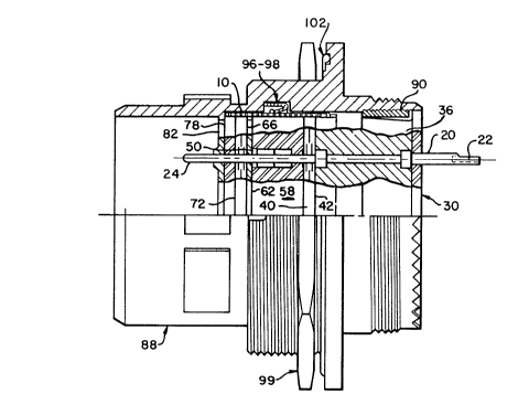
Figs. 1 - 3 show the details of the grounding cylinder 10
of the filter connector of the invention. Cylinder 10 is
1~9Z7~6
-- 4 --
formed from a conductive strip 12 provided with a number of
tabs 14 along top and bottom edges and a number of fastener
holes 16. The tabs 14 in this embodiment conform to the
configuration of the outer surface of the "pin array" -
namely, the electrical connector contact pins with filteringelements to be described.
Fig. 2 shows that cylinder 10 is formed from a blank
consisting of a foil thickness, which thickness is only that
necessary to provide support strength to the pin array as will
be described.
Fig. 3 shows the cylinder 10 in its formed configuration
for encircling a hereinafter defined pin array not only to
strengthen the pin array but also to permit the conductive
strip 12 being placed into electrical contact therewith. In
this embodiment, cylinder 10 is made from a beryllium copper
alloy having a foil thickness such that the formed cylinder is
strong enough to support the more fragile elements of the pin
array, as well as pass to ground stray electrical currents
induced in the shell of the connector.
Fig. 4 shows in partial section one embodiment of the
multi-pin electrical filtering connector of the invention.
This embodiment is a circular, jam nut style configuration,
although the invention is not limited to this configuration.
The filtering connector typically comprises a
multiplicity of electrical pins (only one pin 20 is shown in
Fig. 4), each having a pin contact end 22 and an opposite end
24. It is to be understood that it is not necessary that all
of the pins 20 be filtered. A mix of filtered pins and
l~Z~786
-- 5
non-filtered pins may fit predetermined certain needs,
although, on occasion, all pins may be filtered.
Positioned near the contact end 22 of pin 20 is a first
non-conductive grommet seal 30, provided with openings for
pins 20 to pass through. The grommet 30 may be made from
electrically non-conductive elastomeric material, such as
fluorosilicone rubber, for example. As used herein,
"non-conductive" and "dielectric" are synonyms.
A dielectric body 36 having openings corresponding to
pins 20 is located after said grommet 30. The dielectric body
36, also referred to as a "first insert", is preferably made
from an epoxy molding compound, such as Epiall* or Fiberite*,
to enclose a portion of said pins 20 and to cushion against
physical shocks.
Positioned in contact with the interior face 42 of insert
36, is a first planar ceramic capacitor array 40 having
openings corresponding to said pins 20. These monolithic
ceramic planar capacitor arrays, either circular or
rectangular, are available commercially, such as MIL-C-38999
circular Planar Capacitor Array series of AVX.
Ferrite inductor beads 50 are mounted on and around each
of the pins 20 which are desired to be filtered. These
ferrite beads are available commercially from several sources.
A non-conductive elastomer body or second insert 58 is
provided with openings to accept each of said ferrite beads 50
mounted on a pin 20 and any non-filtered pins. The second
insert 58 separates physically and insulates the ferrite beads
50 one from another and also from the first capacitor 40.
* Trade Mark
1~9278{~
-- 6
This insulation eliminates arcing between beads or
beads/capacitor.
The elastomer body 58 has positioned against its outer
face 62 a non-conductive interface seal 66, provided with
openings for receiving the pins 20.
Positioned against the face of seal 66 is a second planar
ceramic capacitor array 72, having openings corresponding to
the pins 20.
Positioned against the outer face of the second capacitor
72, provided with openings for the pins 20, is a second
non-conductive grommet seal 78.
After the second grommet 78 there is positioned a second
non-conductive interface seal 82, provided with openings for
the pins 20.
lS A conductive grounding cylinder 10 encircles the elements
depicted in Fig. 4 extending from second grommet 78 to the
first capacitor 40 and beyond to include a portion of the
dielectric body 36. Grounding cylinder 10 unitarily supports
the various elements, as well as providing an electrical path
from the pin array to a shell to be described hereinafter.
The filtering connector includes outer conductive shell
88 for housing the pin array. A retaining ring 90 inside
shell 88 and interior of grommet 30 holds insert 36 within the
shell.
There is supported within shell 88 a conductive ring
element 96 providing a multiplicity of resilient contact
fingers 98 for making electrical contact with the grounding
cylinder 10 and also providing an electrical grounding path
_ 7 _ 1 Z9 ~78~
from the pin array to the shell 88. These rings with spring
contact fingers are available commercially. One such example
is beryllium copper design Q, 97-252:255, of Instrument
Specialties Co., Inc., Delaware Water Gap, PA 18327.
Superior results are obtained when the pin array and the
two capacitors are further bound together. Preferably, each
capacitor and each of said pins are soldered together.
Desirably this is done using a Phase Four Model 1214* Vapor
Phase Soldering System of Dynapert HTE--Emhart, Concord, MA
01742.
In jam nut 99 installations, apertures may permit entry
of stray EMI at the mounting interface. To further ensure
shielding effectiveness at the connector mounting opening,
shell 88 has positioned on and around it a conductive ring
102. Typically ring 102 is a conductive elastomer O-ring.
EXEMPLARY
Six specimens of the filter connector of the invention,
including the vapor phase soldering, were subjected to sine
20 wave vibration in accord with a standard military test.
Visual inspection at the conclusion of each testing revealed
no damage to any specimen.
Specimens were tested and found to be acceptable for
military usage of filter connectors of the invention,
25 including vapor phase soldering, having receptacle shell
sizes: 11, 13, 15, 17, 19, 21, 23, and 25; Mount type: box
mount, wall mount, jam nut; Pin size: 22D and 20; the Filter
Circuit was low-pass Pi-section.
A * Trade Mark
- 8 - ~ ~Z7~6
These specimens displayed:
CAPACITANCE 5000 pf to 15000 pf Q lKHz and +25C
WORKING VOLTAGE 50V, 100V, 200V
5 CURRENT RATING 5 Amps., 7.5 Amps.
R.F. CURRENT CAPACITY 3.0 Amps.
INSULATION RESISTANCE 10,000 Megohms Q +25C.
DIELECTRIC WITHSTANDING
VOLTAGE 300VDC, 500VDC ~ +25C.
10 OPERATING TEMPERATURE -55C to +125C.
ATTENUATION 18dB minimum at 10 MHz.
65 dB minimum at 100 MHz.
, .