Note: Descriptions are shown in the official language in which they were submitted.
~29Z7~8
.
BACKGROUND OF THE INVENTION
The present invention relates to a
semiconductor laser module of the dual in-line package
type suited to be used as a transmitting light source of
a high-speed transmission system having a transmission
rate of 1 Gb/sec or more.
In a conventional semiconductor laser module of
the dual in-line package type, as described in the NEC
technical Report (Vol. 38, No. 2,1985, pages 84 through
89), an input terminal connected to a semiconductor laser
is formed of one of airtight terminals of the dual in-
line type. Such a structure is advantageous in that the
semiconductor laser module can be readily mounted on a
printed board or the like, but has a drawback that it is
difficult to make short the length of the input terminal.
Accordingly, the radiation leakage of a high-frequency
signal is generated at the input terminal, and thus the
frequency of an input signal applied to the semiconductor
laser is limited. In other words, the conventional
semiconduct~r laser module of the dual in-line package
type pays no attention to the connection of the input
terminal to a drive circuit which generates a high-
frequency signal in the order of 1 Gb/sec (that is, in
the giga bit band). Accordingly, the operation of the
2S semiconductor laser module is not
- 1 -
~Z~Z798
satisfactory in the giga bit band.
SUMMARY OF THE INVENTION
It is an object of the present invention to
provide a semiconductor laser module of the dual in-line
package type which is readily applied with a high
frequency signal and can perform a high-speed operation
in the giga bit band, while keeping an advantage that a
dual in-line package can be readily mounted on a printed
board.
In order to attain the above object, according
to the present invention, a semiconductor laser module of
the dual in-line package type comprising: a semiconductor
laser disposed within a dual in-line package; an optical
fiber coupled optically with the semiconductor laser and
extended to the outside of the package; an airtight
terminal connected electrically with the semiconductor
laser; and a coaxial-type high-frequency connector fixed
to the package and connected electrically with the
airtight terminal. Thus, a high-frequency signal in the
giga bit band can be readily applied to the semiconductor
laser through the coaxial-type high-frequency connector,
without degrading the air tightness of the dual in-line
package.
BRIEF DESCRIPTION OF THE DRAWINGS
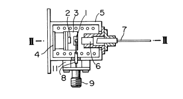
Fig. 1 is a plan view of an embodiment of a
semiconductor laser module of the dual in-line package
type according to the present invention, with parts cut
away.
-- 2
. ' ~
129Z798
1 Fig. 2 is a sectional view taken along the line
II-II of Fig. 1.
Fig. 3 is a plan view of another embodiment of a
semiconductor laser module of the dual in-line package
type according to the present invention.
DESCRIPTION OF THE PREFERRED EMBODIMENTS
Now, explanation will be made of embodiments of
a semiconductor laser module of the dual in-line package
type according to the present invention, with reference to
Figs. 1 to 3.
Fig. 1 is a plan view of one of the embodiments,
with parts cut away, and Fig. 2 is a sectional view taken
along the line II-II of Fig. 1.
Referring to Figs. 1 and 2, a semiconductor laser
1 is mounted on a stem 3 made of oxygen-free copper,
together with a monitoring photodiode 2 and a thermistor
(not shown) for temperature detection. The stem 3 is
fixedly mounted on an electronic cooling element 4 which
is fixed to the inner wall surface of a dual in-line
package 5. The terminals of parts which are not required
to perform a high-speed operation, such as the monitoring
photodiode 2, the thermistor for temperature detection,
and the electronic cooling element 4 are connected to dual
in-line terminals 10. One of the positive and negative
electrodes of the semiconductor laser 1 is bonded, by the
wire bonding method, to an airtight terminal 8 which
penetrates the wall of the dual in-line package 5.
lZ9Z79B
1 The other electrode of the semiconductor laser 1 is
connected to the stem 3. That portion of the wall surface
of the dual in-line package 5 where the airtight terminal
8 exists, has a protrusion 11 for fixing a coaxial-type
high-frequency connector 9 (for example, an SAM-type
connector). The connector 9 is fixed to the protrusion
11 so that the insulated conductor of the connector 9 is
connected with the airtight terminal 8. The stem 3 is
connected to the dual in-line package proper.
According to the present embodiment, a high-
frequency signal can be readily applied to the semiconductor
laser 1 through the coaxial-type high-frequency connector
9. That is, the high-frequency signal is applied to the
semiconductor laser 1 without passing through any one of
the dual in-line terminals 10. Thus, the parasitic
reactance of input terminal and the radiation leakage of
high-frequency signal due to the electrical length of
input terminal are both reduced so as to be out of the
question. Accordingly, the present embodiment can readily
perform a high-speed operation in the giga bit band.
That is, according to the present embodiment, frequency
response characteristics having a cutoff frequency more
than 5 GHz are obtained, and moreover airtightness having
a leakage rate less than 1 x 10 8 atm cc/sec is obtained
which is required to make reliable the operations of the
semiconductor laser 1, the monitoring photodiode 2 and
others.
In the present embodiment, the semiconductor
~Z9Z79B
1 laser 1 is optically coupled with an optical fiber 7 by
means of a focusing rod lens 6. Alternatively, an
optical fiber which is formed with a spherical shape so
as to function as an optical lens may be substituted for
the optical fiber 7, or one of a spherical lens, a convex
lens and a combination of plural lens may be disposed
between the semiconductor laser 1 and the optical fiber 7.
Further, in the present embodiment, the SMA-type connector
is used as the coaxial-type high-frequency connector 9.
However, the coaxial-type high-frequency connector 9 is
not limited to the SAM-type connector, but coaxial-type
high-frequency connectors such as a BNC-type connector,
an N-type connector and an APC-7 type connector may be
used in place of the SAM-type connector. Further, a
coaxial cable may be fixed to the protrusion 11 and
connected to the airtight terminal 8, in place of the
connector 9.
Fig. 3 shows another one of the embodiments.
In the present embodiment, an impedance matching circuit
or a tip resistor 12 having a resistance of 43 ohms and
serving as an impedance matching line is inserted and
connected between the airtight terminal 8 and the coaxial-
type high-frequency connector 9 to obtain the impedance
matching between the semiconductor laser 1 and a drive
circuit connected to the coaxial-type high-frequency
connector 9. Thus, the reflection of input signal from
the semiconductor laser 1 is suppressed, and a favorable
result is obtained. In Fig. 3, the tip resistor 12 is
-- 5
~Z9Z798
1 used as the impedance matching means for the sake of
simplicity. The tip resistor 12 may be replaced by a
circuit or transmission line having a desired impedance.
In this case, also, the present embodiment can perform
an excellent high-speed operation in the giga bit band.
As has been explained in the foregoing, a
semiconductor laser module of the dual in-line package
type according to the present invention can readily perform
a high-speed operation in the giga bit band while keeping
advantages that a dual in-line package is excellent in
airtightness and can be readily mounted on a desired board
or substrate.