Note: Descriptions are shown in the official language in which they were submitted.
~92~02
-- 1 --
PERSON~L r~lEMORY CARD
sackground of the Invention
. _
This invention relates to smart cards and more
particular to a smart card which interacts in a
communication or processing system through a contactless
interface.
2. Description of the Prior Art
The use of credit cards for purchases and for
banking and other transactions has become so popular
that most travelers today do so with very little cash.
The card, typically made of plastic embossed with an
account number and the name of the account owner, serves
solely to identify an authorized account at a bank or
credit house to be charged for a transaction. A
magnetic stripe on the back of some cards contains the
same information, but is machine-readable to speed the
transaction. ~11 accounting information is stored at
the bank or credit house.
In that transactions generally occur at a
location remote from the bank or credit house, it is
easy for a person to use a misappropriated card, or for
a legitimate owner to inadvertently exceed his credit
limit. Most merchants, therefore, require that before
purchases above a relatively modest amount such as
$50.00 are completed, the authorization must be verified
with the bank or credit house as appropriate. Even with
automatic telephone dialing, the procedure is cumbersome
and time-consuming. Furthermore, a separate card is
needed for each account.
With the advent of recent advances in
microelectronics, however, it is now possible to put a
vast amount of computing power and memory right in the
card to produce a "smart card" or "personal memory
card". The card could, therefore, carry personal
identification data to virtually eliminate Eraudulent
use -- such data as personal characteristics, driver
~
- lZ~ 02
license, social security number, personal identification
numbers, and even a voice print. ~!he card could also
carry the account numbers of all of the owner's charge
accounts, the balances of all of the accounts, the
credit limits of all of the accounts, and other such
personal data as, for exanple, the sizes of family
members for clothing purchases, personal telephone
directories, etc. The types of personal data are
li.nited only by one's imagination.
The technology for putting all of this on the
standard size card is here. What is holding up this
very convenient card, however, is what at first appears
to be the mundane problem of a suitable interface for
supplying operating power to the card and reliably
coupling data to and from the card.
Smart cards known in the art are being read
and written into by various contact methods. One
problem that arises if metallic contacts are used,
however, is increased ohmic resistance due to the
oxidation that takes place over time on the contact
surfaces. This is of concern since the accuracy of the
data transfer between a card and a reader or writer
device decreases as the ohmic resistance of these
contacts increases. In addition, the contacts, while in
the exposed position, allow air-borne particles to
deposit on the surfaces decreasing the contact area and
causing intermittent connections. Inasmuch as operating
power for reading and writing into a card is also
transferred from an associated station in a system to
the card via these contacts, there is a loss in the
amount of energy transferred after some time of use,
rendering the card inoperative.
A second problem associated with the use of
metallic contacts in providing operating power and data
onto the smart cards is the possibility of electrostatic
discharge (ESD) occurring which can damage the
microelectronics on the card. High voltages that build
122~0Z
up on a person or card or that are inadvertently coupled
thereto from other sources may very easily be coupled
directly to the electronics on the card when metallic
contacts are used. Clamping diodes employed at the
various inputs of a card provide some measure of
protection, but are not capable of protecting against
some of the higher voltage levels a card might
occasionally encounter during normal use in its expected
environment.
Summary of the Invention
In accordance with the invention, a personal
memory card typically the size of a standard plastic
credit card may be used in a variety of applications,
from custom repertory dialing to storage of individual
medical and/or banking records. Although the card looks
and feels much like an ordinary credit card, the
personal memory card includes a computer, an
electrically erasable field programmable read-only
memory, and also circuitry for receiving a combined
power and timing signal and for receiving and
transmitting data signals between the card and a
reader/writer located in an associated station. No
direct ohmic electrical contact is made between the card
and the reader/writer for transferring power to the card
or data to and from the card. Power to the card and
data to and from the card are therefore reliably
transferred even after some time of use. In addition,
the potential of damage from electrostatic discharges to
electronics in the card is minimized since an insulator
in the form of a dielectric is provided between the
conductors on the card and any sources from which this
discharge might occur. The personal memory card is also
selectively reprogrammable by an authorized user at the
associated station with new and different data as
desired.
~9a~
In accordance with one aspect of the invention there
is provided a portable data card including memory means for
storing data and processor means for processing data, the data
card comprising: input/output means for communicating with at
least one reader/writer station, the input/output means
including capacitive coupling means for transferring data from
the reader/writer station to the data card and from the data
card to the reader/writer station; energy coupling means for
receiving magnetic energy transmitted from the reader/writer
station and for converting the magnetic energy into electric
energy for energizing the memory means and the processor
means; and the capacitive coupling means and the energy
coupling means providing in combination a complete
communication interface between the data card and the
reader/writer station.
.~
~9~0Z
Brief Description of the Drawing
The invention and its mode of operation will
be ~ore clearly understood from the following detailed
description when read with the appended drawing in
which:
FI~. 1 is a functional block representation of
a personal memory card and a reader/writer operative in
accordance with the principles of the present invention;
FIG. 2 shows the basic structure of the
personal memory card and the placement of the major
components thereon in accordance with the principles of
the present invention;
FIG. 3 shows a schematic diagram illustrating
in greater detail the major functional components of the
analog interface circuit depicted in the memory card of
FIG l; and
FIG. 4 shows a schematic diagram illustrating
in greater detail the major functional components of the
reader/writer of FIG 1.
Throughout the drawings, the same elements
when shown in more than one figure are designated by the
same reference numerals.
Detailed Description
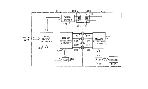
Referring now to FIG. 1, there is shown a
block diagram of a portable data or personal memory
card 10 being employed with a card reader/writer 15 in
accordance with the invention. Some of the principle
components located in the card 10 are a
microcomputer 110, an electrically erasable programmable
read-only memory (EEPRO~) 115, an analog interface
circuit 300, the secondary winding 121 of a transformer
120, and capacitive plates 125 through 128.
The microcomputer 110 includes a central
processing unit and memory units in the form of random-
access memory and read-only memory. A microcomputer
available from Intel Corporation as Part No. 80C51 may
be used for microcomputer 110 with the proper
- ~28V2
programming. Operating under firmware control provided
by its internal read-only memory, the microcomputer 110
formats data to the EEPRO~ 115 and to the reader/writer
15 via the analog interface circuit 300. The
microcomputer 110 also interprets commands from the
reader/writer received through the analog interface 300.
In addition, the microcomputer 110 checks for errors in
reading and writing data to the EEPROM 115 and in
transmissions to and from the reader/writer 15.
~y employing EEPRO~ 115 in the card 10, an
authorized user has the ability to reprogram certain
sections of the card while at an authorized associated
application station with new and different data as
desired. Such a memory is available from a number of
suppliers, many of whom are mentioned in an article
entitled "Are EEPROMS Finally Ready To Take Off?" by J.
Robert Lineback, Electronics, Vol. 59, No. 7,
(February 17, 1986), pp. 40-41. Data may be written to
and read or erased from an EEPROM repeatedly while
operating power is being applied. When operating power
is removed, any changes made to the data in the EEPROM
remain and is retrievable whenever the card 10 is again
powered.
The analog interface circuit 300 provides a
means for interfacing the memory card 10 to the
reader/writer 15. This interface performs a multitude
of functions including providing operating power from
magnetic energy coupled from the reader/writer 15 to the
card 10, and also coupling data between the
reader/writer 15 and the microcomputer 110 in the
card 10. Power to the card lO is provided from the
reader/writer 15 to the analog interface circuit 300 via
an inductive interface provided by the secondary
winding 121 of a transformer 120. This transformer is
formed when this secondary winding in the card 10 is
mated to a primary winding 122 in the reader/writer 15.
lZ~2~z
The transformer 120 may advantayeously include a
ferrite core 123 in the reader/writer for increased coupling
between the transformer primary winding 122 and secondary winding
121. A second such core 124 may also be included in the
transformer 120 and associated with the secondary winding 121 in
the card for a further increase in coupling efficiency. In those
arrangements where ample power is available and efficiency is not
a consideration, one or both of these cores may be omitted. The
use of a transformer for coupling power into a credit card was
proposed by R.L. Billings in U.S. Patent No. 4,692,604 which
issued on September 8, 1987.
Data reception to and data transmission from the card
10 are provided to the analog interface 300 by a capacitive
interface comprising four capacitors formed when electrodes or
plates 125 through 128 on the memory card 10 are mated with
corresponding electrodes or plates 155 through 158 in the
reader/writer 15. Two of these capacitors are used to tra,nsfer
data to the memory card 10 from the reader/writer 15 and the
remaining two are used to transfer data to the reader/writer 15
from the card 10. The combination of the inductive interface and
the capacitive interface provides the complete communication
interface between the reader/writer 15 and the memory card 10.
The analog interface circuit 300 is shown in greater detail in
FIG. 3 and further described in the accompanying description
later herein.
The organization of some of the components in the
reader/writer 15 functionally mirror those in the card. Such
components are, for example, an analog interface circuit 400 and
a microcomputer 410. In addition, the reader/writer 15 also
includes a power supply 162 and an input/output interface 160.
The power supply 162 is used to provide power and also to couple
a clock signal from the reader/writer 15 to the card 10
()2
through the transformer 120. The input/output
interface 160 is principally a universal asynchronous
receiver transmitter (VART) and may be advantageously
included in the microcomputer 410. This VART used for
externally communicating with a suitably configured
application station.
With reference to FIG. 2, there is shown the
basic structure of the card 10 and the relative
placement of the principal components thereon. The card
generally comprises a laminated structure including a
0.005 inch thick single or double sided printed wiring
board 201. Capacitive plates 125 through 128 are shown
deployed on the top side of this printing wiring board,
but it is understood that it is well within the
capabilities of one skilled in the art to deploy these
plates on the bottom or opposite side of the board as
long as they are covered by a suitable insulator or
dielectric sheet. Pads for bonding the analog interface
circuit 300, microcomputer 110~ EEPROM 115, transformer
secondary 121 and surface-mounted capacitors 302 and 315
are located on the top side of board 201. The
intergrated circuits, i. e., the microcomputer 110,
EEPROM 115 and analog interface circuit 300, are wire
bonded and the capacitors are conductively epoxied to
the printed wiring board 201. It is to be understood
that other means of electrically connecting the
integrated circuits to the printed wiring board 201 are
known to those skilled in the art. Tape automated
bonding is an example of one such means.
In the construction of the card 10, the
printed wiring board 201 has laminated to it a
structural member 202 which is approximately 0.020
inches thick. This structural member has multiple
openings 203 to accommodate the physical size of the
above mentioned components which are mounted to the
printing wiring board 201. A potting material is
subsequently applied in sufficient quantity in the
VZ
-- 8
openings 203 of the structural member 202 to cover the
components located therein and build up the slightly
depressed upper surface of each of these components to
align with the topmost surface of the structural
member 202.
A top cover sheet 204 is laminated to the
structural member 202. To this cover sheet an
appropriate label and logos are either affixed thereto
or embedded therein. A dielectric sheet is also
laminated to the bottom side of the double sided printed
wiring board 201 thereby covering up the conductor leads
(and possibly conductive plates) located on the lower
side of this board that would otherwise be exposed. It
is this lower exterior side of the card that generally
has instructions and also a magnetic stripe and
signature panel as desired.
Referring next to FIG. 3, there is shown in
greater detail the analog interface circuit 300 of
FIG. 1. A number of functions for the memory card 10
are provided by this interface circuit, such as power
rectification and regulation, transmitting data to and
receiving data from the reader/writer lS, obtaining a
clock signal from the transformer secondary 121 for
operation of the microcomputer 110 and also providing a
power reset operation for resetting this microcomputer
whenever power is removed and then reapplied to the
memory card 10.
Magnetically coupled from the reader/writer 15
through the transformer 120 to the secondary winding 121
is an approximate 1.8 megahertz AC signal. The output
of this secondary winding 121 is applied to a full wave
bridge rectifier 301. The DC voltage generated by the
bridge rectifier 301 is filtered by a capacitor 302 and
then coupled into a two-part regulator 303 which has a
shunt regulator section on the front end and a series
pass regulator on the back end.
lZ~Z~il02
g
The shunt regulator serves to keep the current
drawn out of the transfonner secondary winding 121
fairly constant and thereby insures operation in an
optimal area on the power transfer curve of
transformer 120. This is desirable, since if the power
demand in the card 10 decreases, the shunt regulator
section dissipates the extra power to keep the load
constant on the reader/writer 15 and on the transformer
secondary winding 121 which is receiving the AC p~wer.
And if the power demand goes up in the card because an
operation that requires greater power is occurring, the
shunt regulator section reduces its power dissipation
when it detects the voltage decreasing. The current
then passes through the series-pass voltage regulator
and provides operating power for all of the other
circuitry in the card. Capacitor 315 provides
additional filtering to the DC output of the shunt and
series pass regulator 303.
A clock recovery circuit 304 is coupled to the
secondary winding 121 of the transformer 120 for
providing a clock signal suitable for operation of the
microcomputer 110. This circuit 304 comprises a
comparator which differentially compares one side of the
secondary winding 121 of the transformer 120 relative to
the ground node of bridge rectifier 301. The pulses
that are provided are shaped by the comparator giving
relative fast turn-on and turn-off times suitable for
driving the microcomputer 110.
A reset circuit 305, comprising a voltage
reference 306, a comparator 307 and a monostable
multivibrator 308, monitors the regulated output of the
shunt and series pass regulator 303. This circuit
inhibits the operation of the microcomputer 110 if the
supply voltage at the output of the shunt and series
pass regulator 303 is not within a predetermined
operating range.
1;~9~802
-- 10 --
A resistor string comprising resistors 309 and
310 form a divider circuit which reduces the voltage
coupled to the comparator 307 from the regulator 303.
And the voltage reference 306 sets a threshold voltage
level corresponding to the minimum allowable of the
required operating level which is then compared with the
voltage from the resistor string in comparator 307. In
operation, as the voltage from the shunt and series-pass
regulator 303 rises from zero, the voltage provided to
the comparator 307 from the voltage reference 306 is
higher than the voltage provided to the comparator from
the resistor string and the microcomputer remains reset.
When the voltage from the shunt and series-pass
regulator 303 rises above the minimum operating voltage,
the output of the resistor string becomes higher that
the voltage reference. The comparator 307 then switches
states and the monostable multivibrator 308 provides a
pulse of approximately 200 milliseconds in length to the
microcomputer 110 which is enabled thereby and a
processor contained therein starts running.
If some time after reaching the required
operating level, the regulated voltage happens to dip
below the threshold voltage level, the reset circuit 305
detects this decrease and again inhibits the
microcomputer 110. This insures against extraneous
operations which might occur and in some way affect the
data in the EEPROM 115. The reset circuit 305 thus
causes the microcomputer 110 to be inhibited whenever
the voltage is less than the predetermined operating
voltage and therefore guards against improper operation
of the card 10 in such low voltage state.
Such an incorrect voltage could occur possibly
because the card 10 is not fully seated into the
reader/writer 15 or if there is too much of a gap
between the surface of the card 10 and the mating
surface in the reader/writer 15 because of some
obstruction lodged on either surface. And since any
l2~2~n2
interruption of the voltage to the card also causes the
reset circuit 305 to be activated, occurrences such as
an interruption of AC power to the reader/writer 15, or
a user pu]ling the card 10 out of the reader/writer 15
at an inappropriate time will also cause the
microcomputer 110 to be inhibited. Operation of the
microcomputer 110 is resumed once the supply voltage
returns to the proper operating level.
~ data out drive circuit 311, comprising
driver amplifiers 312 and 313, receive serial data from
the microcomputer 110 and differentially drive the
capacitive plates 125 and 126 which, respectively,
interface with the capacitive plates 155 and 156 in the
reader/writer 15. These drivers 312 and 313 convert the
serial data from the microcomputer 110, which is of one
polarity, into a differential polarity such that for
each transition of the signal from the
microcomputer 110, one of the drivers goes positive,
while the other goes negative.
~ data receive circuit 320 is comprised of a
differential amplifier and is used in receiving
differential data coupled to the capacitive plates 127
and 128 from capacitive plates 157 and ]5~3 in the
reader/writer 15. This data from the reader/writer 15
25 is coupled to the microcomputer 110 in the card 10 Eor
the appropriate processing. Hysteresis is built into
the data receive circuit 320 such that a differential
pulse greater than the hysteresis is all that is
required to switch the output of the amplifier from a
high state to a low state or from a low state to a high
state. The hysteresis aids in preventing noise from
causing false triggering of the data receive circuit by
ignoring small differential noise signals and switching
only on large differential data signals. Thus once the
data receive circuit switches states, if there is no
further input, it will remain in whatever state it is
then switched into and not drift back to the other
1~9Z~OZ
- 12 -
state.
Although ESD problems are minimized with a
contactless card, the addition of protective diodes to
clamp the voltage on the outputs of data drive circuits
311 and the inputs of data receive circuit 320 may be
designed and included in the card circuitry. The design
of such clamping circuits for clamping and also
integrating voltages to safe levels is well known and
within the capability of those skilled in the art.
Referring next to FIG. 4, there is shown a
schematic diagram illustrating in greater detail the
major functional components of the reader writer 15
shown in FIG. 1. The memory card 10, shown
schematically in FIG. 1 and graphically in FIG. 2, is
shown in FIG. 4 in operable contact with the data and
power couping components of the reader/writer 15. Power
to the card is provided from the reader/writer 15 via
the primary winding 122 of the transformer 120 formed
when the secondary winding 121 in the card 10 is mated
to the primary winding 122 in the reader/writer.
As earlier indicated, the transfer of data
between the reader/writer 15 and the card 10 is provided
by a capacitive interface formed when plates 125 through
128 on the card are mated with corresponding plates 155
through 158 in the reader/writer 15. The reader/writer
15 has a number of components comparable in operation to
those found in the memory card 10. Like the card 10,
the reader/writer 15 includes a data-out drive circuit
comprising non-inverting driver amplifier 401 and
inverting driver amplifier 402. These amplifiers
receive serial data from a UART 403 and differentially
drive the capacitive plates 157 and 158 which interface
with the capacitive plates 127 and 128 in the card 10.
Data for the memory card ]0 is transmitted to the UART
in parallel arrangement over an 8-bit bus 411 from a
microcomputer 410.
12~2~0Z
- 13 -
The reader/writer 15 also includes a data
receive circuit 404 which is comprised of a differential
amplifier and is used by the reader/writer 15 in
receiving data coupled to the capacitive plates 155 and
156 from the capacitive plates 125 and 126 in the card
lQ. This serial data from the card 10 is coupled to the
VART 403 where it is reformatted into parallel data and
then coupled to the microcomputer 410 over the 8-bit
data bus 411. The microcomputer 410, through use of an
internal U~RT reconverts the data into a serial format
with start and stop bits before coupling the data to a
particular application station 440 with which the
card 10 and reader/writer 15 are configured to
communicate.
The application station may comprise a number
of confiqurations. It may be configured as a factory
editing station, an office editing station, an issuer
editing station, public telephone station, or any other
station suitably configured for interacting with the
card 10.
Circuitry for efficiently controlling the
transfer of power into the card 10 is advantageously
included in the reader/writer 15. ~ power driver 420
controls the power level that is transmitted into the
primary winding 122 of the transformer 120. The power
provided to the card 10 via the transformer secondary
winding 121 is proportional to the current in this
transformer primary winding 122. The amount of power
being provided to the card 10 at any given time by the
driver 420 is sampled in the transformer winding 122 and
the information is provided to the analog-to digital
converter 421. This converter provides to the
microcomputer 410 a digital signal equivalent of the
sampled analog power level. The microcomputer 410, in
turn, adjusts the power going to the card 10 to the
desired drive level with a signal provided to a
digital-to-analog converter 422. The output of this
Z~Z~302
- 14 -
digital-to-analog converter is coupled to a voltage
regulator A23 which provides continually corrected drive
power for the card 10 into the power driver 420. In
this way, power into the card 10 is controlled to within
the desired range for proper and efficient operation.
Using a card with the reader/writer 15
requires inserting the card in an accomrodating slot in
the reader/writer 15. In order to insure proper mating
between the card 10 and the interface components within
the reader/writer 15 and also to insure correct turn-on
of the reader/writer circuitry, proximity sensors are
located in the slot in the reader/writer 15. .~ card-in
sensor 425 is located approximately half way in the card
slot. This is an optical sensor with illuminating and
detecting elements. A mechanical arm is arran~ed to
interrupt an optical beam generated by the illuminating
element and being detected by the detecting element as
the card progresses approximately half-way into the
slot. This card-in sensor g25 provides a signal to the
microcomputer 410 once a card is at the halfway point on
its way in or on its way out of the station.
A card fully-in sensor 426 is comparable to
the card-in sensor in operation, but is located in the
innermost part of the card slot. This sensor informs
the microcomputer 410 when the card is fully seated in
the card slot.
The reader/writer 15 is conveniently designed
to accommodate not only personal memory cards with
reprogrammable microelectronics therein, but also cards
that have only a magnetic stripe affixed thereto. Once
a card is fully seated, a test is performed to determine
if the card is a contactless personal memory card or a
card having only a magnetic stripe. This test is
initiated by having the microcomputer 410 apply power to
the power driver 420. If power is drawn from the
transformer primary winding 122, the reader/writer 15
assumes a memory card is in the slot. Otherwise, the
1~9Z~02
- 15 -
reader/writer assumes that a magnetic stripe card
occupies the slot.
Once the card is fully inserted and if
determined to be a memory card based on the current
drawn by the transformer primary 122, a solenoid 427 is
activated by the microcomputer 410 in order to bring the
communication interface in the reader/writer 15 in
contact with the inserted card. The capacitive plates
155 through 158 and transformer primary 122 comprising
this interface are mounted on a platen for deflectably
positioning against the card by this solenoid in order
to get the best capacitive and inductive coupling with
the card. If the card fully-in sensor 426 is ever
tripped because the card is partially pulled out, the
solenoid 427 releases immediately so that the card can
be easily withdrawn.
If the test for a memory card proves negative,
the microcomputer 410 decides that the card just
inserted is a magnetic stripe only card. The
microcomputer 410 then provides an audible or visual
signal to the user to remove the card. AS the card is
pulled from the slot, data on the magnetic stripe is
read by a magnetic head 430, amplified by an
amplifier 431 and then coupled into a serial port on the
microcomputer 4]0.
Included in the reader/writer 15 is an
oscillator section 435. This section provides a clock
signal for the microcomputer 410 and also provides an
approximate 1.8 megahertz signal for the power
driver 420. It is this signal that is detected by the
clock recovery circuit 304 in FIG. 3 in order to provide
a clock signal suitable for operating the
microcomputer 110 in FIG. 1.
A clock signal for the data transfer circuitry
is also provided by the oscillator section 435 to the
UART 403. This signal sets the data transfer rate
between the card 10 and the reader/writer 15 at 19.2
--\
12~2~02
- l6 -
kilobits per second. Such a data rate keeps the
capacitive plates properly biased during the intervals
between data bit transitions and thereby minimizes the
susceptibility to noise in the communication interface
between the card and the reader/writer due to voltage
drift.
The microcomputer 410 has additional memory in
the form of an external random access memory (RAM)
section 437 and an external read only memory (ROM)
section 436. For ease of updating or reprogramming, the
ROM section may be easily replaced or augmented with an
EEPROM section. Such an EEPROM section in the
reader/writer 15 and/or in the station 440 is easily
reprogrammed by data contained in a card when the card
is brought in operable contact with the
reader/writer 15.
As earlier indicated, the microcomputer 410
communicates with the outside world via a serial data
path to the station 440. This data path includes a
transmit lead 441 and a receive lead 442. It also has
an attention lead 443 which is activated by the card
fully-in sensor 426. Finally, it also includes a reset
lead 444 which enables the station 440 to reset the
reader/writer 15 and initialize it into a known state.
Power to the reader/writer 15 is also supplied by the
station 440.
Many other modifications of this memory card
are possible and may obviously be implemented by those
skilled in the art without departing from the spirit and
scope of the invention. An example of such a
modification is a memory card operating in a system
wherein data is communicated only from the memory card
to a card reader. The memory card and/or an associated
card reader are configured to have the minimal
communication interface and microelectronics necessary
to establish and maintain the flow of data from the card
to the card reader. It is therefore to be understood
lZ92~
- 17 -
that within the scope of the appended claims the
invention may be practiced otherwise than as
specifically described.