Note: Descriptions are shown in the official language in which they were submitted.
i ~9~5
MOSFET FULL~RIDGE SWI~CHING REGULATOR H~VING TRANSFORMER
COUPLED MOSFET DRIVE CIRCUIT
BACKGROUND OF THE INVENTION
.
PIE~D OP THE INVENT~ON
.
Thi~ in~ention relates to power supplies and more
particularly to a voltage regula~or having an FET inverter
stage and an improved driver circuit for that stage.
PR~O~ AR~ .
One typ~ o~ ~wltching regulator which is well known in
the prior art employs a full bridge topology for the
inverter switche~, with each of the four switching devices
being driven by an iqolated ~ignal. The use of ~OSFETS for
thes~ main ~wltches allows lower drive power, but due to the
do~irably fast switching speeds and unavoidably relatively
largc input capacitance, gatc volt~ge ringing can be a
problemO Moreover, power ~witching circuit~ are often
drivan by tran8~ur.~er5 t~ pr~id~ i~olatt~ ~r th~ hi~
voltages ~t r~a~on3bI cost. These transformers introduce
~dditional inductanca~ that.make control o~ gate voltage
v~ry dif~lcult. Als~, the use o~ transformer coupling
batwcen the driver and inverter stages is accompanied by the
well-known problem of transformer core "walking", that is
saturation of the core due to asymmetrical operation
thereof. Prior art solutions to these problems iDclude .
compromi~e~ between switching Prequency and the ~ost of
special magnetic3 designed to r~duce voltage spike , and
anti-walking sche~es which reduce efficiency, increase cost,
or carry with the~ resident problems G~ their own.
KI986-015 ~
'~ :
::
'
.
~:~3~
SUMMARY OF TIIE INVENTION
It is a general object of the invention to provide an
improved power supply having topological ~eatures which
overcome the aforede~cribed problems of the prior art in a
rellable and economical manner.
The3e and other objects of the invention are achieved
by a power supply which provides a transformer coupled drive
system for an FET Bridge Regulator that -horts the
transform~r primary during OFF ~ime of the main switches of
the regulator. Thi~ shorting removes the effects of the
large magnetizing lnauctance and the associated energy fro~
the secondary clrcuit of the trlnsformer. with ~he
trans~ormer shorted, the secondary L/C circuit, consisting
of the main switch gate capacitances and the transformer
leakage and wiring inductances, is much more easily damped.
The drive circuit operates from two, interleaved input
signals provided by regulator control circuits of the power
supply. ~hese signals may have duty cycles ranging from O
to nearly 50~. Each lnput pulse produce~ positive gate
signals to one diagonal pair of main switches and negative
gate signals to the other palr. When both inputs are O~P,
all main ~witchea arn biased OFF.
Accor~in~ t~ on~ aspect ~f ~h~ i~vention, a~ FE~
brid~e regulator has a ariving transform~r for the gates of
the power FETs of th~ requlator, and a driving circuit for
the primary o~ the driving transformer, the driving circuit
comprising a full bridge formed by first and second sets o~
drlving FETs, which include diodes for revexse, drain-source
conduction, each qQ~ c~mpri~ing a complementary pair of FET5
ana being connected across the transformer primary, one FET
of each ~et being driven ON to together form a conducting
path connecting a voltag~ source across the primary o~ the
transformer and in the ab~ence of driving signals one
. .
.
R~986-015 - 2 -
I .
. ~ .. . . . . . . ., , .. .... ... . ~ . . . ..... .
1~93~95
transistor of each pair conducts forwardly and one conducts
rever~ely to e~tt~lish a short circuit across the primary.
According to still another aspect of the invention, the
voltage supply for the driving FETS in the driving circuits
of the primary of the driving trans~ormer includes a
resistance across which there is developed a voltage
proportional to the current drawn by the driving transformer
primary in each half cycle of ita operation, whereby the
voltage applied to that primary is reduced asymmetrically in
a corrective direction when the currents drawn during the
respective half cycles are not equal.
The fosegoing and other objects, features and
advantages of the invention will be apparent from the
following speci~ication and the drawings forming a part
thereof.
BRIEF DESCRIPTION OF THE DRAWINGS
Fig. 1 is a block diagram of a power system including
driver and inverter stage~ in accordance with the inventlon~
Fig. 2 i8 a ~implified circuit diagram of the driver
and inverter stage~ of the power system of Flg. 1.
Fig. 3 i a set of curves representing drive circuit
~olta~e wa~ shap~s ~LLustrati~ o~ the ope~atLnn ~ the
dxiver stage shown in Fig. 2.
Fig. 4 is a ~et of curves representative of current
~aveshapes in the operation o~ the drlver stage of Fig. 1,
for time periods corresponding to those of FigO 3.
Fig3. Sa thru Sd, show paths of control current and
load current during periods "In- through "IV" of the
operation as shown in Figs. 3 and 4.
Fig. 6 shows a simplified equivalent circuit
representative o~ principles i~volved in the operation of
the ~irc~it of Fig. 2.
~I986-015 - 3 -
` ~
~ .
~93~5
Fig. 7 shows ~ set of curves illustrative of the
"walking" pro~le~.b solved in accordance with an aspect of the
invention.
Fig. 8 shows a fragmentary detail showing an
alternative embodiment of the damping network connected to
the gate drives o~ the main switch scheme of Fig. 2.
DETAILED DESC~IPTION
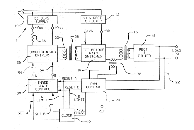
Fig. l shows a power supply system which in gross
aspects ls similar to many conventional power supply
-~ystems. That is, energy derived from an A.C. Source 10 is
rectified and filtered at 12 and the resulting D.C~ i.s
chopped by switche~ 14 into pulses which are delivered via
power transformer 16. to a recti~ier and filter arrangement
18 which deliver~ regulated and smoothed D.C.. to the useful
load 20. Typlcally, in .~uch a system, regulation is
achieved by a feed~ack loop 22 including a pul~e width
modulation control 24 by which the driver circuits 26 of the
main ~witches 14 are operated in such manner as to vary the
width of the pulses delivered to 16 in a manner to
compensate for error detected by the loop 22 at the terminal
~upplying the load 20.
In th~ By~tem shown, the main ~witches .camprise a
br~d~e arran~ement o~ ~ield effcct-tra~sist~rs~P~5J driven
v~a a transformer 28, and the dr~ver3 26 are arranged in a
cl~cuit whereby they respond to a three-s~ate control 30 in
accordance with the invention to drive the primary 32 of
transformer 28 in opposite directions with deadtimes
therebetween during which the primary 32 is short-circuited.
Also, in accordance with the invention, ~he complemen~ary
drivers 26 are .energized via a source 34 which includes
means such as a resi.~tor 36 operable to apply voltages to
the drivers in accordance with an inverse func~ion of their
respective current loadq.
.
~ .
KI986-015 - 4 ~
. ., , .~ ~ ... . ..... ... ., ~ .. . . . ... . . ... ... . . ... .. .... ... ... ... . . . ......
~2932~
The pulse width modulation control 24 in the
illustrated embod:ment utilizes a ramp signal derived from a
curren~ transformer 38 in series with ~he primary of the
power transformer 16. The ramp signal is compared with an
error signal, developed by comparing the output DC voltage
detected by 22, to yield a Reset A or Reset B signal as
determined by an ~/~ phase signal emitted by a clock unit
40. Clock 40 al~o pro~ides A Limit and B Limit signals
which act as supplementary A Reset and s ~eset controls.
Clock 40 also proYides Set A and Set B signals to the three
Sta~e Control 30. That Control 30 comprises latches which
are set and reset ~o yield signals A and ~ as will be
de~cribed.
Fig. 2 shows simpllfied circuit diagrams iilustrative
of a preferred embodiment of ~he driver 26 and main switch
14 sections of the power supply of Fig. l.
The circuit arrangem~nt shown in ~ig. 2 uses four
small, low voltage MOS~ET's M5, M6, M7, MB, the sin~le drive
transformer 28, and ~ive resistor~ 78, 80, 82, 84, and 36 to
achie~e the overall function when operated by the signals A
and ~ from the three state control 30 o~ Fig. l.
Transistor M5 i9 a P-channel device the source S of
which i5 re~renced ~ia canductor 50 t~ + Vcc }e~ any drop
acras~ rosi~tor 3~, and transistar M7 is an N channel device
thc ~ource S of which is referenced to -Vcc via conductor
52_ the gates G of transistors M5 and M7 are connected
tog~ther and via conductor 54 to control input A O r the
three state control 30 (Fig. 1). The drains D of
transistors M5 and M7 are connected .together and to one
termina7 56 of the pr~mary 32 of the driver transformer 28.
~ he control signal applied at terminal A by the three
state ~ontrol 30 is referenced to a "zero" volt le~el equal
to -Vcc so that when the signal at terminal A is up
XI986-015 - 5 -
.
: .- . - . ..........
~?3;~9~
~positive) transistor M5 is OFF and transistor M7 is 0~,
thereby disconn^~ting terminal 56 from conductor 50 and +vcc
and connecting terminal 56 to conductor 52 and -Vcc.
Transistor M6 is a P channel device the source S of
which is referenced via conductor 60 to IVcc less any drop
acros3 resis~or 34, and transistor M8 is an N channel device
the ~ource S of which is referencea to -Vcc via conductor
62. The gates G of transistors M6 and M8 are connected
together and via conductor 64 to control input B of the
three state control 30 (FigO 1). The drains D of
transistors M6 and M~ are connected together and ~o the
other terminal 66 of the primary 32 of the. .driver.
transformer 280
The control signal appl~ed at terminal B by the three
state control 30 i referenced to the same ~zero" level
e~ual to -Vcc as i~ the above described "A" signal, so that
when the signal at terminal ~ is up tpositive) transistor ;~6
i3 OFF and transistor M8 i3 on, thereby disconnecting
terminal 66 from conductor 60 and +Vcc and connecting
terminal 66 to conductor 62 and -Vcc.
When the slgnal at terminal A is down ~zero), ~he gate
G of transistor M5 is at -Vcc turning M5 ON, and the gate G
of trAn~istor ~7 is at approximately the ~ame potential as
its sourc~ S, depr~in~ . sate.. drive an~ turning
transistQr M7 OPF. 5imilarlyr when the signal at t~rminal B
1Y down, transistor M6 is ON. and transistor M8 is OFF.
Figure 2 al80 shows a basic embodiment of the main
witch .~tage 14 in accordance with the invention. Four
MOSFET tr.ansistors Q1, Q2, Q3, Q4 are connected in a full
bridge ~onfiguration to gate pulses of current from the ~VB
terminal o~ bulk DC source 12 to the main power transformer
16. Gate drive for the main switch transistors Ql, Q2, Q3,
Q4 is provided by respective secondaries 70, 7~, 74~ 76 of
driver transformer 28 in response to energization of primary
KI986-015 - 6 -
.... . _ ... . ..... _ .... ... ............ .. . .. .
.... .... ,.... ~ .... .. ~ .. . . . ... .. .
~Z93~2~5
32 of that transformer, as will be described. Addition~lly,
resistor~ 78, 8..~, 82, 8~ are provided across the respective
drive secondaries 70, 72, 74, 76; tha~ is, between the
source and gate terminals o~ the respective main transistor
switches Ql, Q2, Q3, Q4.
Circuit operation will now be described with the aid of
waveshapes shown in Fig. 3 and 4, and the current paths
.illustrated in Figs. 5a through 5d~ Inputs V(a) a~d V(b)
are the signals from the control circuït terminals A and B,
Figs 1 an~ 2. These signals are alternately ON positive,
have essentially equal ON times and equal timing between the
beginning of each pulse. When V(a) 1~ positive, as shown a~
100, Fig. 3, drive switch M7, Fig. 2, is-ON and MS is OPF.
M6 will be ON due to the zero level of V(b) which is
negative relati~e to the source terminal S of M6. .This
result$ ~n a positive primary voltage v(p) at terminal 66
relative to terminal 56, and positive ga~e signals to main
switch transistor3 Q1 and Q4. The other two main switches
tQ2 and Q3) will have negative gate voltages as indicated by
the dotting on -qecondaries 72 and 74, and hence will be OFF.
The drive transformer 28 will have a primary current I(p),
~igs. 2 and 4, as a result of re~lected load current in
re~istor3 7~, 80~ a2, a4, and due to magnetizin~ curre~t in
tra~rs~ormer 2~_
When V~a) return~ to zero, as shown at 102, Fig. 3, ~7
w$11 turn OFF and MS will turn ON. M6 remains ON. V~p) and
~11 main gate signalq from secondarie~ 70, 72, 74, 76 now
drop to zero, stopping conduct~on in all main switches Q1,
Q2, Q3, Q4. The magnetizing current established in
trans~ormer 28 during the ON time must continue to flow.
This current, shown at 104, Flg. 4, will flow through
transistors M5 and M6 resulting in an effective
short-cixcuit on the primary winding 32. This shorted
primary condition is reflected to the secondasies 70, 72,
KI986 015 - 7 -
......... .... . ,. .. ... , ~ .. ~ ..... , ...... .. ..... ~ . ... ... . . . ........ .. .. . . .
3 ~32~
7~, 78 as a low impedance across al~ gate-source terminals
of the main swi~ches Ql, Q2, Q3, Q4, holding them OFF.
When V(b) at terminal s, Figs. 1 and 2, goes positive
as shown at 110, Pig. 3, circuit operation is reversed. M6
turns off, M8 turns on, V(p) is negative an i(p) through
primary 32 reverseY as shown at llZ, Fig. 4. Main switches
Q2 and Q3 now conductO The magnetizing current in 28
decreases and reverses. When v(b) returns to zero, as shown
at 114, Fig. 3, M8 turns OPF, M6 turns ON, and the reversed
magnetizing current, shown at 116, Fig. 4, flows in M5 and
"backwards" through M6. The shorted primary condition is
established again and alI main switches Ql, Q2, Q3, Q4 are
held o~fO
Figs. Sa-5d trace the current flow in portion I, II,
III ! ~V of the above de~cribed cycle of operation. These
fiqures relate to the voltage and current curves of Figs. 3
and 4 in accordance with the portions I, II, III, IV
delineated thereon.
If the ON (i.e., up) tlmes of V(a) and V~b) are equal,
the magnetizing current and core flux of drive transformer
28 will center around zero. nence, the peak fl-lx in
transformer 28 will be one half of the total flux excursion.
If the A and B signals from the control circuits do not hav~
exactly thQ ~am~ ON ti~e, ~cor~-walki~g-n or asymm~tricaI
magnetLc cycling of the core of transformer 28 may result,
leading to non-symmetrical magnetizing current. Under these
condlti~ns~ the ~oltage drop across resistor 36, Figs. 1 and
2, durlng the ON time3 of signals A and ~ will be different,
tending t~ reduce the voltage on primary 32 of transforDer
28 during the longer ON time and t-o increase the primarv
voltage or the shorter ON time. Volt-time unbalance on
tran former 28 i~ thu3 li~ited by the drop acro~s resistor
36. Resistox 36 also serves to limit the peak current in the
drive switches which occurs when M5 and M7 (or M6 and M8)
XI986-015 - 8 -
~3Z~g~
conduct simultaneously during the transitions of v(a) (or
V(b)). Althougk the internal resi.stances of ~5, M6, M7 and
M8 also con~ribute to the pea~ current limiting and
transformer anti-walking, the external resistor 36, which
has a value significantly greate~ than the operating
internal resi3tance of the MOSFETS M5 through 8,
predominates in thi effect and does not limit the
magnetizing currents 104, 116 durin$ OFF times of ~he drive
control.
Figs. 6 ana 7 summari~e the op~ration of dri~er section
26 of Figs. l and 2. Transi=tors M5, M6, M7, and M8 of Fig.
2 are represented ~y a double pole, triple ~hrow switch lZO,
each pole havinq three positions 1, 2, 3. Position
correspond~ to the ~, not B input condition position 2 to
not A, not ~ condition~ and position 3 to the B, not A
condition. In the position 1 shown, conventional current
flows fro~ +Vcc through balancing resistor 36' to primary
32' terminal 66', through 32' to primary terminal 56', to
-Vcc. This state is represented at portion I of the family
of curve~ of Fig. 7. Switch position 2 corresponds to
portion~ II and lV o f Fig. 7, and switch position 3
corresponds to portlon III of Fig. 7.
As sh~w~ in ~ d l~ne in FigO 7 durinq state Qr cur~e
port~ns ~ an~ . Irr c~rr~nt ip through prtmary 32' shouId be
~irror images of each oth~r. Core 28' "walks", i~ a shift,
delta t, occurs in Vp and ip as shown in dotted line.
However, this undesirable condition is corrected by the
d~fferential voltage drop in balancing resistor 36'. When
the primary current during operation portion I starts to
exceed its norm, a~ shown at delta i, curve portion I, the
drop across resistor 36' reduces Vp by delta i times the
resistance va~ue of 36', thereby reducing vp durin~ that
portion I of the operation s~ as to bring the operation back
XI986-015 - 9 -
1~3~
into balance or at least restrain it from further drift from
balance. ~
The values o~ resistors 78, 80, 82, 84 are dictated by
the amount of damping required in the secondary circuits
driven by transformer 28. The critical time occurs at the
end of the ON time when gate signals of two of the main
switches Q1, Q4 or Q2, Q3 fall, initiating turn-off. Gate
signals to the other main switches go from a negative
voltage to zero and, in fact, overshoot positive due to
leakage inductance of transformer 28 and gate capacitance of
the main switche~ Ql-Q4. If turn-off of the ON main
switche~ Q1, Q4 o~ Q2, Q3 is slow and tha positive ove~shoot
exceed~ ~he thxeshold voltage on the OF~ devices, both main
switches Ql, Q3 or ~2, Q4 on one "leg" of the bridge conduct
forming a short circuit across v(b). The values of
resistors 78, 80, 82, 84 must be reduced to limit this
overshoot to voltages less than the main switch turn-on
~hreshold voltage.
Reducing the values of 78, 80, 82, 84, however,
~ncrea~es the prim~ry current and power dissipation in drive
sw~tche~ MS, M6, M7, M8 and all resistor~. An alternative
approach to provide damping of the maln gate signals is to
introduce series resi3tor3 130 as ~hown in Fig. 8. For the
usual ran~ ~f leakag~ inductanc~ a~d sate- ca~cita~ce
encountered, small value~ of ~eries resista~ce have a major
impact on circuit damping. Henae, the positive overshoot
probl~m can be c~ntrolled without sig~ificant increase in
primary current and overall power dissipation.
The drive circuit must also contend with transient
voltages produced by drain voltage excursions of the main
switche~ Ql-Q4. Of particular interest is the negative
excursion on the dsain of a main switch caused by switching
of the other device in the same leg. ~his occurs at nearly
the same time as the positive overshoot discussed above.
~I986-015 - lO -
.
~Z~3~9~i
.,
The effect is to produce a negative "spike" on the gate due
to coupling tl.rough the drain-gate capacitance. The
amplitude of this spike must be limited to values less than
the gateosource voltage rating. ~educing the values of
resi3tors 78, 80, 82, 84, will reduce the amplitude of this
spike but at the same ~cost" as above - i.e., increased
primary current and overall power dissipation. Note that
the introduction of the series resistors alone will increase
the spike amplitude.
Also shown in Fig. 8 are additional elements co~prising
an alternative circuit to 11mit the spike voltage. A
clipping networ~ composed of a diode 132, resistor 134 and
zener diode 136 may be added to each main switch gate
circuit (Q1 i5 shown~ which wiil ~clip" the negative spike
at approximately the zener voltage. This voltage would be
selected to be greater than the normal drive voltages bnt
well below the gate-source voltage rating. During positive
gate pulses, diode ~32 blocks. During negative gate pulses;
diode 132 conducts, allowing zener diode 136 to clip the
volt~ge.
Speclfic deslgns may, or may not, require the series
resi~or and/or clipping circuitry, dependent on transformer
lea~age, ~OSFET gate characteristics, and wirinq parasitLcs
or t~ade-~ff'~ ~ circuit complexity ~. co~trol bias power
and overall power ~i~sip~tio~ may fa~or the use o~ one or
both o~ these alternative circuits.
In the foregoing, a current mode control of the ON
times of the A and ~ signals is achieved by use o ramp
signals derived by means of the current transformer 38 from
the current in the primary of the power transformer 16, in
other words, the main switch current rises as energy is
delivered to inductance in the output filter of section 18
during the A and ~ ON times. Alternatively, this ramp
fu~c~io~ could be provided by a saw tooth generator in the
~I98S-015 - 11 -
.
lZ~325~S
control 24. Both control schemes are well-known. Moreover,
the drive circui~ 26 may be adapted to provide the drive
function in other regulator topologies such as dual switch,
half bridge, and push-pull configurations. Also, alternate
connection of the P and N channel drive switches is possible
and still achieve equivalent operation. Accordingly,
although one main embodiment of the invention has been shown
and described in detail, it will be apparent that the
invention is not limited thereto~ but could be otherwise
embodied within ~he cpirit of the invention and the scope of
the appended claims.
,
.
.
RI988-015 - 12 -
t