Note: Descriptions are shown in the official language in which they were submitted.
-- 1 --
The present invention relates to thyristors
(including a light-activated thyristor) with an over-
voltage self-protection function of punchthrough type
and, more particularly, to a thyristor manufacturing
method which can precisely realize the breakover voltage
at which the punchthrough occurs and is particularly
used for manufacturing thyristors used for a high-
voltage conversion application in direct-current power
transmission.
In the field of high-power thyristors used for
high-voltage converting applications, thyristors with
overvoltage self-protection function have been develop-
ed. Many of the thyristors with overvoltag~ protection
are of the avalanche type. This type of thyristor is
described in "Controlled Turn-on Thyristors", by VICTOR
A. K. TEMPLE, IEEE, Trans. Electron Devices, ED-30, pp.
816-824 (1983) GE.
In the case of this avalanche type, formed ln a
part of the P gate-base layer of a thyristor of PNPN
structure ls a region in whlch avalanche breakdown is
; more likely to occur than other parts. In the operation
of ovérvoltage~protection, the avalanche-breakdown first
occurs in the region by means of a transient voltage at
; the rise of an overvo1tage and thus a nondestructive
current flows through the region with the result that a
~: :
; pilot thyristor is turned on and subsequently a main
thyristor is turned on~to decay the overvoltage, thereby
::
~Z9~33~
protecting the tllyristor.
In an intermediate process oE Ina[lufacture of
avalanche -type devices a gate-base region for avalanche
breakdown is formed. ~l~len co~nplet~d, therefore, tile
devices will hav~ varying breakov~r voltages because
of variations in Inaterial or irl process. Since the
avalanclle volt~ge has positive t~lnperature dependency,
the breakover voltage naturally has temperature
dependency. ~rhis Ineans tllat the breakover vol-tage is
higher at room temperature than at higl1 temperature,
making it difficult to design thyrlstor devices,
particularly in the respects of their withstanding
voltages and dl~dt ratings.
~ thyrlstor with overvoltage self-protection of
punchthrough -type ls dlsclosed in a paper entitled
"LASER TRIMMING OF TEIYRISTORS TO ADD AM OVERVOLTAGE
~ SELF-PROTECTED TURN-ON FE~TURE" by J. X. Przybysz, IEEE
; l9a5, pp. 463 - ~68.
: In the discussion of the prior art, reference will
,~ :
; ~ be made to the accompanying drawings, in which:-
Figs. l~ through lE show principal manuEac~uring
processes for a punchthrough type thyristor;embodying
the~present lnvention, more speci1cally, Fig. lA s~o~s
a state of the thyristor prior to the formation of a
recess 20, Fig.~lB shows a state after tlle formation of
; ~ recess 20, Pig. lC shows the state ln ~ ich~a prede;ter-
mined amount of boron ions is implanted in-to the bottom
;~ 20a of recess;20~, and Fig. lE shows a sectional
structure o~ the complete punchthrough type thyristor;
"~
~::: : :
- 2~ Z~33~
Figs. 2~ t,hlougll 2C are reference diagrams for
theoretically exp]aining th~ ground for the present
:I.nventiorl;
Fig. 3 is a sectional view of a thyristor which
corresponds to tlle thyristor ShOWII in Fig. lE and is
manufactured without the use of the rnarl~lfacturing method
of the present invention;
Fig. 4~ shows a sectional structure model of the
punchthrough type thyristor;
Fig. 4B is a graph showing the relationship be-tween
-the breakover voltage Vbo and the distance WpB from
recess bottom 20a to ~unction 11 of the model of
Flg. 4A; and
Fig. 5 shows a modification of the thyristor of
Fig. lE in which the recess 20 has the shape of the
letter "V" in section.
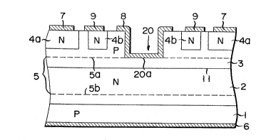
~ Fiy. 3 shows a modification of a punchthrough type
thyristor illus-tra-ted in Fig. 2 on page ~6~ oE the above
paper, to which the present invention is not applied,
This device comprises a main thyristor having a four-
layer structure comprised of a P emitter layer 1, an N
base layer 2, a P gate-base layer 2 and N emitter layers
4a; a pilot thyristor having a four-layer structure
comprised oE P emitter layer 1, N base layer 2 and P
~ga-te-base layer 3 whiFh are all co~mon to the main
: ~ :
"
: `
: :
334
-- 3 --
thyristor, and N emitter layers 4b surrounded with N
emitter layers 4a; and a recess 20 of a gate portion
surrounded with the pilot thyristor. Reference numeral
6 denotes an anode electrode, 7 a cathode electrode, 8 a
gate electrode, and 9 an amplifying gate electrode (a
cathode electrode of the pilot thyristor).
In this punchthrough type, a space-charge layer 5
(the region between broken lines 5a, 5b) is formed in a
junction 11 between P gate-base layer 3 and N base
layer 2 by a forward voltage applied to the thyristor,
and this region 5 extends with an increase in the
forward voltage. When the forward voltage is increased
to the breakover voltage (hereinafter referred to as the
self-protection breakover voltage) at which the self-
protective operation starts, the boundary 5a of space-
charge layer 5 reaches bottom 20a of the recess of P
gate-base layer 3 so that the punchthrough occurs.
Consequently, the current flowing through junction ll
acts as a gate current of the pilot thyristor ll, 2, 3,
4bj to turn it on. Immediately after the pilot thyris-
tor is turned on, the main thyristor ~1, 2, 3, 4a) is
.
safely turned on, thereby protecting the main
thyristor.
Space-charge layer 5 extending to P gate-base
25~ region 3 becomes narrow because the impurity
concentration of layer 3 is much higher than that of
N base~2. Although being possible in the stage of
3~3~
-- d,. _
laboratory, therefore, the precise control of the self-
protection breakover voltage is very difficult to attain
from the viewpoint of mass productivity.
Fig. 4A shows a structure model of a punchthrough
type thyristor, while Fig. ~B is a graph showing the
relationship between a distance WpB from bottom 20a of
the recess to junction 11 and a breakover voltage Vbo at
which the punchthrough occurs in P gate-source layer 3.
As can been seen from Fig. 4B, the breakover voltage Vbo
varies greatly as the distance WpB varies slightly. It
will thus be Eound that the precise control of the self-
protection breakover voltage is difficult to attain.
(It is to be noted that, in Fig. 4B, WpB is represented
by the linear scale, while Vbo is represented by the
logar1thmic scale.) The distance WpB varies with the
profile of the impurity concentratlon of the P gate-base
layer.
To solve the above problems, it is required to
determine the depth of the recess for each of thyristor
pellets, for example, by monitoring them with a
~voltmeter~ in order for the P gate-base layer below the
recess to accurately cause the punchthrough at a self-
;protection breakover voltage.
As described above, the problems with the conven-
tional method of manufacturing thyristors wikhovervoltagc self-protection are that: it is difficult to
determine the self-protectlon breakover voltage with
:
1~93~34
precision in intermediate processes of manufacture; and thus
the co~plete devices have great variations in their breakover
voltage. The method utilizing the voltmeter for monitor can
solve the above problems, but is not suitable for mass
production because many manufacturiny processes are involved.
It is accordingly an ob~ect of the present invention to
provide a thyristor manufacturing method which can mass-
produce a thyristor, in which variations in the self-
protection breakover voltage are small, at substantially the
same manufacturing yield and cost as in the case of
production of an ordinary thyristor.
The invention will now be described in more detail, by way of
example only, with reference to the accompanying drawings
introduced above.
Accordingly therefore the present invention provides a method
of manufacturing a semiconductor device with overvoltage
self-protection, comprising a four-layer structure extendiny
from a top surface to a bottom surface of a semiconductor
substrate and including an emitter layer of one conductivity
type, a gate-base layer of an opposite conductivity type.
base layer of said one conductivity type and another emitter
layer of said opposite conductivity type, said method
comprising the steps of: a first step of making a recess in
said gate-base layer from its surface exposed to the top
~5 surface of said substrate, the depth of said recess being
such that the bottom o~ said recess reaches at least a space-
charge layer produced in said gate-base layer when a
predetermined forward voltage is applied to said
semiconductor device, and further extends close to a junction
between said base layer and said gate-base layer a second
step of doping said semiconductor substrate with impurities
of said opposite conductivity type from the bottom of said
recess to form a region under said recess having an impurity
- 5 -
33~4
concentration lower tllall said gate-base layer, the amount of
said ;mpurities being substantially equal to ND X 1
(atoms/cm2) which is the product of the depth 1 (cm) of the
space-charge layer produced in said base layer when the
forward voltage is applied to said semiconductor device and a
concentration ND(atoms/cm3) of impurities of said one
conductivity type in said base layer; and a third step of
forming an electrode on the surface of said recess.
For a better understanding of the present invention, a method
for attaining the above object will be described with
reference to an embodiment of Fig. 1 in which one
conductivity type is N type, while an opposite conductivity
type is P type.
The present invention is directed to a method of
manufacturing a semiconductor device with overvoltage self-
protection of punchthrough type. The method comprises the
following steps in manufacturing a thyristor having a four-
layer structure of N emitter layers 4a, 4b, a P gate-base
layer 3, an N base layer 2 and a P emitter layer 1.
(a) A step of making a recess 20 in P gate-base layer 3 from
its surface exposed to the top surface of
~ - 5a -
3~
-- 6 --
a substrate. In this step, recess 20 is formed to the
depth in which a space-charge layer produced in gate-
base layer 3 when a predetermined breakover voltage Vbo
for self-protection is applied to the thyristor reaches
at least bottom 20a of the recess, and bottom 20a of the
recess extends close to the junction between gate-base
layer 3 and emitter layer 2.
~b) ~ step of introducing P type impurities from
bottom 20a of the recess to gate-base layer 3 to form a
region 3x of low impurity concentration just under
bottom 20a of the recess. The amount (atoms/cm2) of the
P type impurities is substantially equal to ND X ~ which
is the product of the depth ~ (cm) of the space-charge
layer produced in the N base layer when the breakover
voltage is applied to the thyristor and the impurity
concentration ND ( atoms/cm3) of N base layer 2.
(c) A step of forming an electrode 18 on the
surface of recess 20a.
The amount (atoms/cm2) of the P type impurities
~20 introduced from the bottom of the recess is defined
as the amount per unit area (cm2) of the junction
surface.
The present invention utilizes the following
functlons of a thyristor.
when a predetermined forward voltage Vbo equal
to a self-protection voltage is applied to a thyristor,
a re~erse voltage that is substantially equal to the
~: :
~ ~3 ~3~
forward voltage is applied across junction 11 between P
gate-base layer 3 and N base layer 2 whereby space-
charge region 5 is formed to extend on either side of
junction 11. The product ND x ~ (atoms/cm2) of the
depth ~ (cm) and the impurity concentration ND
(atoms/cm3) of the space-charge layer on the side of N
base layer 2, that is, the amount (atoms/cm2) of
impurities per square centimeter of the space-charge
layer on the side of the N base layer becomes equal to
the corresponding amount (atoms/cm2) of impurities of
the space-charge layer on the P gate-base layer. In
addition, if the forward voltage Vbo and ND are deter-
mined, then ND X ~ will be found from theoretical
calculation. Hence, it is possible in mass-producin~
processes to make the amount of the P-type impurities in
the P~-type ~ate-base layer 3x extending from bottom 20a
of the recess (on the surface of which electrode 18 is
formed) to a portion of ~unctlon ll that is ~ust under
: : ~ the recess substantially equal to the ND X ~. In such
a thyristor, the punchthrough occurs in P~-ga~e-base
Iayer 3x under bottom 20a of the recess at the forward
voltage Vbo. ~ ~
~: In the present invention, the bottom 20a of recess
20 is formed near to junction 11 between base layers 2
: ~ 2s and 3. That is, the recess is formed so that its bottom
~: :
20a may reach a region, within a transition re~ion in
which the conductivity type changes from P type to N
:
3333~
type, in which the amount (atoms/cm2) of impurities per
unit area of ~unction 11 under bottom 20a of the recess
becomes negligibly small as compared to ND x ~. In the
present invention, therefore, the self-protection
breakover voltage Vbo at which the punchthrough occurs
is determined by the amount of impurities per unit area
of junction 11, which are introduced from the bottom 20a
of the recess. The depth of recess 20 has no direct
effect on the breakover voltage Vbo. The amount of
impurities to be introduced is precisely controlled by
the use of an ion implantation technique, for example.
Th~s the variations in the self-protection breakover
voltage can be reduced significantly.
The ground for the inventlon will be described.
Figs. 2A and 2B show the density of electric charge p
and electrlc field E in a PN stacked ~unction with
reverse bias. Fig. 2C shows the position X0 of the PN
junction, the end X1 of a space-charge layer on the side
of P-type layer and the end X2 of the space-charge layer
,
~ ~ 20 on the side of N-type layer. The axis of abscissa
:
represents the distance X in the direction normal to the
:: : :
plane of the junction. In Fig. 2A, Xp and Xn represent
the partial widths of the space-charge layer (depletion
layer) in the P- and N-type layers of the ~unctlon~
~respectiveLy, and hence the total width of the space-
charge layer is W = Xp ~ Xn. The electric-char~e
denslty p is given by the product of the charge q
~333~
g
(absolute value) of an electron and the impurity
concentration. Thus, the p-type and N-type layers have
an impurity concentration of ~qNA and qND, respectively.
The electric charges qNA x xp and qND x Xn of the P and
N layers per unit area of the ~unction in the space-
charge layer are equal to each other. Fig. 2B shows the
distribution of the elactric field which is obtained by
integrating the distribution of the electric charge in
Fig. 2A. The width of the space-charge layer obtained
when a predetermined reverse voltage is applied can be
found on the basis of the distribution of the electric
field.
It is required that the amount of impurities ~P~)
under bottom 20a of the recess be negligibly small as
compared to the amount of P-type impurities of ND x Xn
(atoms/cm2) which are introduced after the formation of
recess 20 shown in Fig. 2C, so that a p~ layer 3x of
very low impurity concentration may be formed. More-
over, taking NA ND into conslderation, recess 20 must
~e formed to the depth very close to PN junction 11 in a
transition region from P type to N type.
In usual thyristors, a portlon of an N-type
substrate is used for the N base layer, and the P gate-
base layer is formed by diffusing impurities from the
ma~or surface o~f the su~strate. Hence such an ideal
abrupt ~unction~as shown in Fig. 2A cannot be formed.
~The P and N layers are equal to each other in the amount
:: :
~a333~
-- 10 --
oE electric charges per unit area ln the space-charge
layer so -that q~l~Xp = q~l~X~I. IE the self-protection
voltage Vbo is determilled, then ~I~Yp tiill be found
from -theoretical calcu].ation. Xn can tllus be calculated
from Vbo and ~ID as X~ Xp/~lD. Tlle alllount (qNDXn) oE
electric charges per Ulli.t area of P~ ~.ayer 3x under -the
bottom of the recess in the space-charge layer can also
be found.
This invention will llOW be descri.bed in more
detail, by way of example only, with reference to the
drawinys introduced above.
~ :::
; ~ :
~ : :
3~3~
~ s sho~n in Fig . 1~, P-type impuritles are diffused
in an N-type semiconduc-tor substrate 2 Erom its ma~or
surfaces (the upper and lo~er surfaces in the Figure) to
form a P emi-tter layer 1 and a P gate-base layer 3.
Furthermore, N-type impurlties are selectlvely diEfused
in P gate-base layer 3 using a mask not shown to form N
emitter layers 4a for a maln thyristor and N emltter
layers for a pilot thyristor. Thus, a our-layer struc-
ture of MPNP in ~hich a portion of N-type substra-te 2 is
used as N base layer 2 is obtained.
Subsequen-tly, as shown in Fig. lB, a layer 12 of
oxide (sio2) is formed over the ma~or surface ~the upper
surface of the Figure) o~ the substrate on the side of a
cathode and then a recess 20 is formed by the use of the
oxide layer as a mask. The formation of recess 20 may
be performed by a laser processlng technique, a wet
:
~333~
- 12 -
etching technique, a dry etching technique such as CDE,
a grindstone processing technique or a combination
thereof. In this embodiment, recess 20 can be formed by
the grindstone cutting and subsequent light wet etching.
The depth d of recess 20 is such that its bottom 20a
reaches a space-charge layer 5 produced in P gate-base
layer 3 when the self-protection breakover voltage vbo
is applied to the thyristor. Moreover, the bottom 20a
of the recess is at a position, within a transition
region (3x~ o conductivity type from P type to N type,
the impurity concentration at which is negligibly low as
compared wlth the amount of impurities, such as boron
ions, introduced by a subsequent process, for example,
below 1ol5 atoms~cm3. If this requirement is met, the
bottom 20a of recess 20 may go under junction 11.
Further, if this requirement is met, recess 20 may be of
a V shape in section as shown in Fig. 5.
Next, the amount (atoms/cm2~ of P type impurities
13, which is;equal to the product ND x ~ (atoms/cm2) of
the impurity concentration Nd (atoms/cm3) of N base
layer 2 and the depth ~ (cm) of space-charge layer 5
produced in N base layer 2 when the self-protection
::
voltage is applied to the thyristor as shown in Fig. ~B,
~ is introduced into the bottom of the recess as shown in
Flg. lC. It is desired that the amount of impurities be
precisely controlled by the use of an ion implantation
technique. The impurities 14 may be any of P-type
: ~ :
:~
3~
impuritie~ such as boron ox garium.
Subsequently, as shown in Fig. lD, the activation
and diffusion of the implanted ions of boron are
performed by heat treatment to form a desired PN
junction 21.
Next, as shown in Fig. lE, after the surface of
recess 20 is covered with a layer 17 of molybdenum
silicide (MoSi2), an anode electrode 6, a cathode
electrode 7, an amplifying gate electrode 9 and a gate
electrode 18, which are all made of aluminum, are formed
by a conventional method. Aluminum is usually used for
the gate electrode.
In order to provide good ohmic contact between
aluminum and silicon, if aluminum is sintered at a high
temperature to produce a layer of alloy A~-Si, the
amount of impurities under bottom 20a of recess 20 which
has been precisely controlled would differ because of
th~ layer of alloy. For this reason, it is desired that
a metal such as molybdenum silicide (MoSi2), which does
not make a layer of alloy with sllicon at a sintering
temperature of alumlnum, be formed on the surface~of
recess 20 before the evaporation of aluminum. Instead of
:: : : ~:
MoSi2, a sllicide of Ti, Ni, or V may be used.
When a forward overvoltage is applied to a thyris-
~ tor manufactured as described above, and a transient
voltage occurring at the rise of the overvoltage reaches
the sel~-protectlon breakover voltage Vbo, the
:: :
:: : :
:: :
punch-through occurs in the recess 20. As a result, a
current resulting from the punchthrough flows into the
gate of the pilot thyristor (1, 2, 3, 4b3 to turn it on,
and the main thyristor (l, 2, 3, 4a) is subsequently
turned on, so that the thyristor is protected from the
overvoltage.
The manufacturing method of the present invention
may be applied to thyristors having no pilot thyristor
structure, ordinary electrically-activated thyristors
and light-activated thyristors.
The conventional manufacturing method for thyris-
tors with overvoltage self-protection of punchthrough
type has dif~iculty in precisely determining the self-
protection breakover voltage vbo in an intermediate
process of manufacture, or is not suitable for mass-
production of thyristors because of the necessity of
monitoring the breakover voltage for each of thyristor
:~ pellets to form recess 20. However, according to the
~: ~ manufacturing method of the present invention, if the
amount:of impurities introduced in the P~ layer of low
:
:impurity concentration under~bottom 20a of the:recess is
: : only controlled, the self-protection breakover voltage
~: : wlth little variation can readily be obtained. Fu~ther,
the amount of impurities introduced from bottom 20a:of
: ~ :
2s : the recess can easily be controlled: by the use of an ion
implantation technique, for example. The manufacturing
~:mPthod of the present invention is suitable for
~333~
- 15 -
mass-productivity and can utilize existing techniques.
Consequently, the present invention can provide a
manufacturing method which can mass-produce thyristors
with little variations in the self-protection breakdown
voltage at the same yield and cost as in the case of
ordinary thyristors.
The use of a thyristor according to the present
invention will save the need of an overvoltage protec~
tion circuit which is provided in conventional equipment
lo and thus decrease the bulk of the equipment. This
provides advantages of cost down and high reliability.
The self-protection breakdown voltage has no temperature
dependency, easing the design of equipment.
~: :
.