Note: Descriptions are shown in the official language in which they were submitted.
3~
70471-6
ACKGROUND OF T~IE INVENTION
The present invention relates, in general, to a test
fixture f0r high speed and power TAB (Tape Automated Bonding) type
semiconductor circuits or devices.
TAB circuits or devices are formed by attaching a
semiconductor circuit die to a supporting film having a plurality
of conductor leads etched thereon. The film contains sprocket
holes similar to those found on a reel of 35 mm film. The circuit
dies or devices are centrally located on the film, and are mechani-
cally and electrically secured to the etched conductor leaas which
fan out to bonding pads along the outside edges of the film.
The testing of semiconductor circuits in TAB type
form presents a combination of formidable engineering problems.
Each of the circuits tested must be subjected to a wide range of
temperatures to insure that they will operate properly over their
full specified range. In addition, electrical connections and
controlled impedance paths to each of the circuits must be provided
~so that all of thelr functions can be properly tested.
The present invention seeks to provide a test fix-
ture which meets these criteria.
SUl~MARY OF THE INVENTION
It is therefore the object of the present invention
to provlde a test fixture for semiconductor circuits, particularly
but not exclusively TAB type high power semiconductor circuits or
devices which provides adequate electrical connections and con-
trolled impedance signal paths to the circuits under test, and can
.
~; :
" ~2~3~31~i
70471-6
control the temperature to which the circuits are exposed over
a wide range.
According to a broad aspect, the invention pro~ides
a test fixture for semiconductor circuits comprising: means to
receive a circuit to be tested; transmission line means having a
controlled impedance to supply power and control signals to a
recei~ed circuit; said transmission line means comprising: a first
circuit board having a characteristic impedance established by a
plurality of conductive paths disposed therein; a plurality of
vertically extending test pins soldered to said first circuit board
and electrically connected to said plurality of conductive paths,
and, a second circuit board disposed on said first circuit board
which includes:
(a) a plurality of vertically extending holes for
reception of said test pins;
(b) a conductive layer plated on a plurality of edges
of said second circuit board to establish a reference plane for
said test pins, and extending along a top surface of said second
circuit board; and,
20 ~ (c) a dlelectric layer disposed on said~top surface
: ~so that;when a received circuit having horizontally disposed con-
ductora is placed on top of said second circuit board, said
conductive:iayer extending along said top surface will establish a
reference plane for the hori ontally disposed conductors of a
received circuit so that the characteristic impedance of the con-
duc~tors is:controlled; means to electrically contact said
- 2 -
::
:: ~::: :: : : : : :
.
~3~3~
70471-6
transmission line means to circuit leads of a received circuit and,
means to vary the temperature to which a received circuit is
exposed.
For use with a TAB type circuit, the ^test fixture
includes in a particular embodiment special circuit boards for
maintaining a 50 ohm transmission line to the '~AB inner lead bond
connections of the circuit, and a thermoelectric heat pump for
controllably varying the operating temperature of the circuit.
The test fixture receives a film slide type carrier
which holds the TAB type semiconductor circuit to be tested. An
anvil is utilized to apply weight on the top side of the TAB film
through a window in the slide carrier to insure that a good elec-
trical connection is made between test pads on the TAB film, and a
plurality of test pins that project vertically from a test fixture
main circuit board disposed beneath the slide carrier.
To maintain a 50 ohm transmission line to the cir-
cuit under test, the main circuit board is provided with a
conventional microstrip design tG supply signals and power to the
test pins. A second smaller special circuit board is provided
to maintain the 50 ohm signal path from the test pins to the inner
lead bond area of the TAB circuit. The circuit board includes
holes for reception of the test pins, and has its edges rnetal
plated to provide a constant voltage reference plane for the pins.
This reference plane also extends along the top surface of the
special circuit board, and runs parallel to the circuit conductors
that are etched in the TAB film from the test pads to the die bond
~ ~ .
- 3 -
~333~
70471-6
connections of the circuit die. A thin dielectric sheet separates
the TAB film conductors from the reference plane. Both of these
reference planes serve to maintain the desired 50 ohm impedance
all the way to the TAs inner lead bond connections of the circuit
under test.
The thermoelectric heat pump is provided to enablé
the circuit under test to be subjected to a complete range of
temperatures to insure that it operates properly over the entire
range. A copper thermal chuck is utilized to provide a thermal
path between the heat pump and the circuit under test, and a large
heat sink is attached to the pump. Through the use of a program-
mable power supply for the heat pump, the circuit under test can
automatically be subjected to a full range of operating tempera-
tures.
The invention may be summarized, insofar as its use
with a TAB circuit is concerned, as a test fixture for TAB semi-
conductor circuits comprising: means to receive a TAB circuit for
testing; transmission line means to supply power and test signals
to a received circuit, said transmission line means including
means to maintai~ a controlled impedance tothe inner lead bond
areas of a received TAB circuit, and comprising:
~(a) a first horizontally disposed circuit board hav-
ing embedded conductors disposed therein for supplying power and
signals to a received circuit, said embedded conductors establish-
ing a characteristic lmpedance for said first circuit board;
(b~ a plurality of test pins positioned to contact
- 3a -
i~:
3 ;33~i
70471-6
the test pads of a received TAs circuit, said test pins being
soldered to said first circuit board, electrically connected to
said embedded conductors, and extending vertically from said first
circuit board; and,
(c) a second horizontally disposed circuit board
placed generally on top of said first circuit board, and having a
substrate with a plurality of holes for reception of said test pins,
said second circuit board including:
(i) a first conductive layer disposed on a
plurality of edges -thereof and including a top portion extending
along a top surface thereof, said first conductive layer establish-
ing a reference plane for said test pins to maintain a character-
istic impedance therefore;
(ii) a dielectric layer disposed over the top
portion of said first conductive layer ~o space a received TAB
circuit fromsaid conductive layer when it is positioned on said
second circuit board, and thereby establish a characteristic im-
pedance for cbnductor leads of a received circuit; and,
(iii) a second conductive layer that is horizon-
tally embedded in said substrate to establish another reference
plane for a received TAB circuit, said second conductive layer
being electrically connected to at least one of said test pins
when said second circuit board is in position on said first circuit
board;
.
weight means to hold the test pads of a received TAB circuit in
secure engagement with said test pins; and means to~ary the
, :
33~
70471-6
temperature to which a received TAB circuit is exposed.
According to another aspect, the invention provides
a test fixture for TAB type semiconductor circuits comprising:
means to receive a TAB circuit for testing, transmission line
means to supply power and test signals to a received circuit; said
transmission line means including means to maintain a controlled
impedance to the inner lead bond area of a received TAB circuit;
means to vary the te~perature to which a received TAB circuit is
exposed comprising:
(a) a heat pump for supplying heat to, and drawing
heat away from, a received circuit; and
(b) a thermal chuck having a top portion for con-
tacting an encapsulated circuit die body of a receive TAB circuit,
and a bottom portion for contacting said heat pump; and,
first weight means to apply pressure to an encapsulated circuit
die body of a received TAB circuit, to firmly engage a received
TaB circuit with said thermal chuck.
BRIEF DESCRIPTION OF THE DRAWINGS
~ ~ The foregoing, and additional objects, ~eatures,
and advantages of the present invention will become apparent from
a consideration of the following detailed descrlption of the pre-
ferred embodiment thereof, taken in conjunction with the accompany-
~ ing drawings in which:
`~ Figures lA and IB, are diagrammatic top and cross
sectlonal side ~iews, respectively, of a TAB circuit and carrier
frame;
~: :
:
- 3c -
:
: :
~Z9333~
70471-6
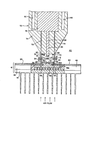
Figure 2 is a diagrammatic cross sectional front
view of the test fixture;
Figure 3A is a diagrammatic partial cross sectional
side view of a special circuit board that forms a part of the test
fixture; and,
Figure 3B is a diagrammatic top view of the special
circuit board.
DETAILED DESCRIPTION OF THE PREFERRED EMBODIMENTS
Turning now to a more detailed consideration of the
present invention, there is illustrated in Figures lA and lB, a
Tape Automated Bonding (TAB) type integrated circuit 10, and a
carrier frame 12 for the same. Circuit 10 includes a clrcuit die
14 that is surrounded by a body of encapsulation material 16,
and ls mounted on a~Kapton film 18.
* Tr~de - ~q rk
:
:
. ~ ~
~ 3d -
.
3336
A plurality o~ conductors 20 are etched on
the film 18, and provide electrical paths between
a plurality of inner lead bond areas 22 of circuit
10 where the conductors are electrically connected
to leads (not shown) of die 14, and a plurality of
test pads 24 that are disposed around the
periphery of circuit 10. A plurality of sprocket
holes 26 are provided in film 18 along two of its
edges which are used in the manufacture and
handling of circuit 10.
Carrier frame 12 is formed from any suitable
material, such as plastic, and is designed in any
suitable manner to securely hold the edges of film
18. A pair of holes 28 are provided in carrier
frame 12 to receive test fixture guide rods that
help align circuit 10 with the test fixture.
Turning no~ to FIG. 2, there is illustrated
a test ~ixture 40 for receiving circuit 10 and
carrier frame 12 in a circuit side down manner
Fixture 40 includes a layered base structure 41
having a heat sink 42 as its bottom layer, which
can be made of any suitable heat conducting
material. If desired, heat sink 42 can be cooled
by forced air from a fan (not shown). Disposed on
top of heat sink 42 near i-ts outer edges, is a
layer 44 of thermal insulation. A thermoelectric
heat pump 46 is disposed on top of heat sink 42 in
an opening in insulation layer 44. The interface
between sink 42 and pump 46 can be coated with a
thermal grease to reduce the thermal contact
resistance.
The thermoelectric heat pump 46 is a known
type of device which is comprised of an array 47
of two heavily doped semiconductor junctions
connected between a pair of smooth ceramic plates.
When a dc voltage is applied to the heat pump, one
plate o~ the pumpj depending on the polarity of
the voltage, will absorb heat at a rate
.
333~
proportional to the current flowing from the power
source. The heat absorbed is transferred to the
other plate and must be removed by some means of
cooling such as heat sink 42. With these devices,
it is possible to obtain differences in
temperature of up to 70 degrees Celsius between
the two plates. Reversing the direction of the
current reverses the heat flow direction. These
devices can therefore be used for both heating and
cooling an ob~ect, and are thus suitable for use
with the present invention, which is designed to
subject the circuits under test to telrperatures
ranging from 20 to 90 degrees Celsius. It will be
understood that any suitable type of programmable
power supply can be used to control heat pump 46 -i
to automatically vary the device temperature over ~:
this range.
~lthough thermoelectric heat pump 46 `5:~
provides an attractive means by which the j~
temperature of a circuit under test can be ~`
variably controlled, the relatively low efficiency
of this type of heat pump indicates that the size
of the pump must be considerably larger than the
circuit to be able to cool it down to the low end
of the specified temperature range. To solve this
problem, a copper thermal chuck or heat spreader
48 is disposed on top of heat pump 46 which
provides a good thermal path between pump 46 and
circuit die 14 when the circuit is in position on
~the test fixture. Chuck 48 is a three tiered
structure that includes a large bottom pedes-tal
48a, a middle pedestal 48b, and a small top
pedestal 48c. Bottom pedestal 48a is attached '"'J
~;~ directly to the top of heat pump 46, while top
pedestal 48c is designed to contact circuit die 14
when carrier 12 is in position.
To provide a cushion, and to correct for any
dimensional mismatches, between circuit die 14 and
~:
33~
'
chuck 48, a thin sheet of thermally conductive
material 50 is placed on top pedestal 48c. This
material is a thermal conductor when placed under
pressure, and consists of a thin metal sheet that
is coated on both sides with a silicon rubber
Such a material is manufactured by the Bergquist
Company of Minneapolis, MN under the name Q-PAD.
Disposed on top of insulation layer 44, and
bottom pedestal 48a, is a horizontally disposed
main circuit board 52, for supplying power and
test signals to the circuit under test. To
maintain a 50 ohm transmission line to the
circuit, conventional microstrip design techni~ues
are employed on the main circuit board 52 by
providing on embedded constant voltage reEerence
plane (shown by dashed lines 53).
A plurality of test pins 54 are soldered to
main circuit board 52 and extend vertisally
through the top of the board as shown. These test
pins are electrically connected to the microstrip
circuitry in board 52 so that they can transmit
power and control signals to the test pads 24 of
circuit 10 when it is in position on the test
fixture.
; A second special circuit board 56 is
horizontally disposed on middle pedestal 48b of
~; thermal chuck 48 and on the inner portions of main
circuit board 52 over pins 54. This special board
:
serves to maintain a controlled 50 ohm signal path
through test pins 54, and all the way to the inner
lead bond areas 22 of circuit 10, and is shown in
greater detail in FIGs. 3A and 3~.
Specifically, in FIG. 3A, there is shown a
partial~cross sectional view of board 56, which
includes an insulating substrate 58. A conductive
layer 60 is disposed on all four edges of
substrate 58. Each of the test pins 54 (one
; shown) passes through a corresponding one of a
r~de rn~fk 6
: ~
3336
plurality of holes 62 disposed in substrate 58, as
illustrated in FIG. 3B. By placing conductive
layer 60 along each edge of substrate 58, a ground
reference plane is established for each of the
test plns 54. In this manner, a controlled
impedance path is obtained along test pins 54,
since each of the pins is disposed parallel to,
and at a fixed distance from, this reference
plane.
Conductive layer 60 also extends along the
top of substrate 58 so that a ground reference
plane will also be established for circuit
conductors 20 when circuit 10 is disposed in
position on top of board 56. Also, a voltage
reference plane is established by a second
horizontally disposed conductive layer 64 that is
embedded within substrate 58. In this manner, a
50 ohm controlled impedance path can also be
established along conductors 20 of circuit 10
between test pads 24, and inner lead bond areas
22. To obtain the desired impedance, a thin
dielectric polymer layer 66 ls disposed over the
top portion of first conductive layer 60 to
control the spacing between conductors 20 of
circuit 10 and the voltage and ground references
planes of special circuit board 56, when the
circuit 10 is in position on the same. If it is
desired to maintain the 50 ohm impedance all the
way past the inner lead bond areas 22 to the
circuit die 14 where the width of conductors 20
reduces as illustrated in FIG. lA, the thickness
of the dielectric layer 66 in that re~ion would
have to be correspondingly reduced as well.
As shown in the top view illustrated in ~IG~
~;~ 3B, special circuit board 56 includes a
rectangular opening 68 in the center thereof so
that the top pedestal 48c of thermal chuck 48 can
make contact with circuit die 14. Also,
: ~ ~
3;;33~
conductive layer 60 is shown as extending to only
a small number of the test pin holes 62 whlch are
labeled 62a. These are the holes which are to
receive the ground test pins.
Two of the test pins holes, labeled 62b, are
also electrically isolated from conductive layer
60, and are connected below to the second
conductive layer 64. These holes receive the
power supply test pins, and provide for capacitive
decoupling of the power supply connections to the
circuit under test. Sheet capacitance is provided
both in the special circuit board 56 and the main
circuit board 52 in this manner by placing both
power signals in circuit board layers that are in
close physical proximity to one another.
Returning now to FIG. 2, a pair of guide
rods 70 extend vertically from thermal chuck ~8
through main circuit board 52. These guide rods
are positioned to pass through the holes 28 in
carrier frame 12 to guide the carrier into
position on the test fixture 40. When carrier
frame 12 is in position, the face down circuit die
14 will rest on top of thermal chuck 48, and, test
~pads 24 will contact the tops of test pins 54.
To insure that circuit die 14 is held with
sufficient pressure against the pressure
responsive thermally conductive sheet 50, and that
test pads 24 make good electrical contact with
test pins~54~,~a two piece anvil 72 is utilized to
apply pressure to these areas of the circuit 10
Anvil 72~includes an outer weight 74, and a center
weight 76, both o~f which are independent of one~;
another so thàt the pressure applied to the test
pads 24 is~independent of the pressure applied to
circuit die 14.
i Disposed in the bottom portion of outer
welght 74,~ are two holes~78 for reception of guide
rods 70. A pair of cavities 80 are disposed in
; 8
::
:: '
:
3~
the upper portion of outer weight 74 that can be
filled with lead beads, or other ma-terial, to
adjust the weight of the outer weight as necessary
to obtain the desired level o~ pressure on test
pads 24. Similar cavities can also be disposed in
center weight 76 iE desired Eor adjustment of its
weight as well.
A pair of silicon rubber strips 82 are
disposed o~ the bottom of outer weight 74, which
are positioned to contact Kapton film 18 of
circuit 10 directly opposite test pads 24. These
rubber strips transmit the weight of outer weight
74 to the test pad/test pin connections, and
accommodate any dimensional mismatches in the test
pins 54.
Anvil center weight 76 includes a narrow
elongated bottom portion 84 which passes through a
centrally disposed opening 86 in outer weight 74.
Disposed-on the end of bottom portion 84 is
another silicon rubber strip 88, which is .
generally the same size and shape as that of
circuit die 14, and is positioned to contact the
encapsulation material directly opposite the die.
Again, this strip accommodates dimensional
mismatches between die 14 and center weight 76,
and transmits pressure from the weight to the die
14 to insure good thermal contact between the die
and the sheet 50, and between sheet 50 and thermal
chuck 48.
From the foregoing, it may be thus seen that
test fixture 40 provides good electrical
connections to the circuit 10 through the use of
test pins 54 and anvil 72. Proper signal
integrity is obtained by maintaining a 50 ohm
transmission line to the circui-t die 14 through
the use of main and special circuit boardq 52 and
56, and their voltage and ground reference planes.
Finally, the temperature of the circuit 10 is
9 '~
~Z~33~
controllable over a wide range through the use of
thermoelectric heat pump 46, thermal chuck 48, and
heat sink 42.
Although the invention has been illustrated
in terms of a preferred embodiment, it will be
understood that numerous variations and
modifications can be made by those of skill in the
art without departing from the true spirit and
scope thereof as ~et forth in the following
claims.
.
:~
:
: ~ :
:::
:`
: