Note: Descriptions are shown in the official language in which they were submitted.
1 r J ~ ~ ~ 7 ~3 3
NEAR-LINEAR SPRING CONNECT STRUCTURE FOR
FLEXI~LE INTERCONNECr CIRCUITS
T~chn1c~ Fie~
Thiæ invention relat~ gen~rally to the electrical
interconnection o~ ~lexiblo (tlex) circuitJ and more
particularly to such interconnect~ whlch ar- espQcially
adapted ror making external electrical connections to ther-
mal ink ~et printhQads.
Backg~ound ~rt
In the manu~actur- Or thin ~ilm r~istor sub-
~trata~ for thermal ink ~t printh~ad~, it is known to
provide heater resistors on a common substrate, such as
silicon, and ~mploy these re~istors to transrer thermal
energy to corresponding ad~acent ink reservoirs during a
thermal ink ~et printing operation. This th~rmal energy
will cause tha ink in the reservoirs to be heated to boiling
and thereby be e~ectQd through an ori~ice ln an ad~acent
nozzle plat~ ~rom which it i~ directed onto a print medium.
During ~uch operation, these heater re~i~tors ar~
electrically pulsed by current applied thereto via conduc-
tive traces formed on top o~ the silicon substrate and
insulated therefrom by an intermediate dieletric layer. The
formation o~ this layer, the ~ormation o~ the resistive
layer for the heater resistor~, and the aluminum evaporation
or sputtering procQss ~or ~orming electrlcal patterns of
conductive trace material to the hsater resistor~ are all
well known in the art and there~ore ~re not de~cribed in
~urthar detail herein. Howev-r, rOr a ~urther discussion of
the various proce~ses used in the ~abrication o~ thermal ink
~et printhead~, re~ersncQ ~ay be mado to the Hewlett Packard
Journal, Volume 36, Number 5, May 1985.
In order to provide electrical connectlons between
external pul Q drlve circuits and these conductive traces on
the th-rmal inX ~et printhead, it ha~ be~n a common practice
to employ 80 callod ~l-xibl- or "rlex~ circuits to make
removeable pres~ur0 contacts to certain conductiv~ terminal
pads on the thin film re~istor prlnthead substrate. For
thi~ connection it becomes nece~sary to provide mean~ by
which pressure can be applled to the ~lexible circuit so
that the electrical leads therein make good electrical
connection with correspondlng mating pads on the thin fil~
rQsistor substrate.
The ~lexible c~rcuit will typically consi~t of a
photolithographically defined conductlve pattern which has
been formed by metal evaporation or sputtering and etching
processes carried out on a thin flexiblQ insulating sub-
strate member. The~e electrical contact locations on the
flex circuit will be raised slightly in a bump and dimple
configuration, and this geometry may be achieved by the use
of a "bed of nails" punch ~tructure whlch match the location
of the dimples. Th$~ structure is used to punch the electri-
cal contact locations on the flex circuit to a raised loca-
tion above the sur~ace o~ the insulating substrate member
thereof .
During thi~ latter punch proce~, it sometime~
happens that not all of the raisQd contact bumps in the
flexible circuit are moved the ~ame distancQ abova the
insulating substratQ sur~ace. For thl~ reason, more force
i8 nece3sary to make contact with the smaller or lower-
height bumps than tho~e highar bumpl mor- extQnded ~rom the
sur~ace of ths ~lex circuit.
one approach to providing the necessary ~orce to
the ~lex circui-t and the necessary prassure contact between
the flex circuit and conductive pad~ on the thin film resis-
tor substrate i9 to use an elastomeric material, such as
rubber, which has been preformed to have a plurality of
cone~ spaced at locations corresponding to the location of
the dimples in the ~lex circult. In thi~ manner, the tip~
o~ these cones can be inserted into the dimples of the flex
~ '7~
circuit and urged thereagain~t with a forcs ~uf~icient to
bring the conductive bumpg on the ~lex circuit in to good
physical and electrical contact with ths terminal pads on
the thin film resistor s~bstrato.
While the above prior art approach to making
electrical contact between tho flex c$rcuit and the print
head ~ubstrate ha~ proven ~ati~ractory for certaln types of
interconnect pattern~ with ~w interconnQct msmbers, it has
not baon entirely s~tisractory ~or connoctlng larger number~
o~ conduc~ivo tracq~ to larger numbors o~ conductivo bumps
or pad~ on the rlex circuit. Thi~ ~act has been a result of
the nature Or the nonlinear de~lection o~ the above ela~to-
meric cone~. This nonlinear do~lection o~ the ela~tomeri~
cone~ i8 seen as a nonllnear variation in cone volumetric
comprQs~ion, Vc, as a function of the distance, D, that the
tip o~ the con- i8 moved during an interconnect operation.
Thus, this nonllnear characteri~tic tend- to increase the
amount o~ ~orc- which must bo appliod to th- ~lox circuit in
ordar to insur- that all the bumps on tho ~lex circuit make
good electrical contact with the conductive traces or
terminal p~ds on the printhead substrato. In somo case~
thia required ~orce i~ suf~iciently large to ~racture the
substratQ or do other structural damage theroto. This non-
linear deflection characteristic of the prior art i~ des-
cribed in mora detail below wlth rererence to the prlor art
7f~3
Figure~ lA and lB
~sclosure or Invent~on
The general purpo e Or thi~ invention i8 to reduce
the amount o~ force required to lnsuro good electrical
contact between a ~lex circuit and a thin ~llm resistor
sub~trate ~or a thermal ink ~et pr~nthead To accomplish
this purpo~e, I havo di~covered and developed a novel,
nearly-linear spring connect ~tructure ror placing the ~lex
circult into good electrical contact wlth contact pads on
the printhead sub~trate with a minimu~ Or rorce applied
thereto Thi~ ~tructur- include~ a central locating msmber
havinq a plurality of cylinders extQndlng integrally there-
through and there~rom to a predeterminQd dl~tance ~rom each
ma~or sur~ac- o~ the central locating member In a
preferred embodiment o~ ths invontlon, cono-shaped tlps are
located at upper endc ot th- ela-tomeric de~lectablo
cyllnder~ and aro in~erted lnto dimpl0- o~ th- ~lexible
circuit with a ~orce ~u~icient to bring the electrical
bump~ or padJ above the dimples into good electrical
contact with matlnq conductive contact pads on the printhead
substrate During this proca~, the volumetric de~ormation
Or the cylinder- varies sub-tantlally linearally as a ~unc-
tion o~ th- ~orce applied to tho lowor endc o~ the~e
cylinders, ~nd this ~eature enable~ the vertical
displacQment o~ the cylinder walls to be maximized ~or a
1~3~7~3
given force applied to these cylinders. In a preferred
embodiment, the cylinders are hollow and are made of
rubber or other like elastomeric material.
Other aspects of this invention are as follows:
A near-linear spring connect structure comprising:
a horizontal central locating member and a plurality of
resilient cylinders extending integrally there-through
or therefrom a predetermined distance from the major
surfaces of said central locating member, said cylinders
spaced laterally apart by predetermined distances
corresponding to predetermined dimensions on a flexible
interconnect circuit at which electrical contact areas
are located, whereby tips of said cylinders may be
brought into forcible contact with said interconnect
circuit to urge said interconnect circuit into
electrical contact with another aligned electronic
structure, and the volume displacement within said
cylinders as a result of force being applied thereto is
nearly linear with respect to said force and thereby
enables the vertical displacement of said cylinders to
be maximized for a given force applied thereto, thereby
minimizing the required force applied to said electronic
structure.
A method of making forced, yet removable, contact
between a printhead or the like having a plurality of
contact pads or areas thereon and a flexible inter-
connect circuit having a corresponding plurality of
contact pads and dimples thereon which comprises:
a. bringing said pads and dimples of said flexible
interconnect circuit into alignment with said contact
pads on said printhead,
b. providing a central locating member having a
plurality of resilient cylinders extending integrally
and perpendicularly therefrom and being laterally spaced
at distances corresponding to the spacings between said
pads and dimples on said flexible circuit, and
1~93~7~3
c. forcing the ends of said cylinders against said
dimples in said flexible circuit~ whereby the volume
displacement of said cylinders as a result of force
applied thereto is nearly linear and thereby enables the
vertical displacement of said cylinders to be maximized
for a given applied force.
A process for increasing both the number and
packing density of mating contact pads on both an
electronic substrate and a facing flexible circuit,
respectively, which comprises the steps of:
a. aligning a plurality of contact pads on a
flexible circuit with a matching plurality of contact
pads on an electronic substrate, and
b. urging a mating plurality of elastomeric
cylinders against said plurality of contact pads on said
flexible circuit, whereby the near-linear spring
displacement of said elastomeric cylinders tends to
minimize the amount of force required to drive all
mating contact pads on said substrate and flexible
circuit into electrical contact, and the lowering of
such contact force enables the number and packing
density of contact pads to be maximized.
Brief Description of Drawin s
Figures lA and lB illustrate the cone shaped
spring interconnect structure of the prior art.
Figure 2 is a graph illustrating the linear versus
nonlinear variations in volumetric displacement of the
cylinder and cone configurations, respectively, as a
function of the variation in distance of compression of
these members.
Figure 3A is a schematic representation of the
spring connect structure-flex circuit-printhead
interconnect scheme of the present invention.
Figure 3B is an enlarged isometric view of one of
the cylindrical interconnects of Figure 3A.
6a
~`
37~3
Figure 4 is an enlarged cross section view of the
compression and bulging of the cylindrical walls
(exaggeratedly spaced) of the elastomeric cylinders of
the spring connect structure of Figures 3A and 3B.
Best Mode For Carrying Out the Invention
Referring now to Figure lA, there is shown
schematically a thin film resistor printhead substrate
10 which has been fabricated using state-of-the-art
semiconductor processing technique and includes a
plurality of electrical-
6b
k~
~ 7 ~3
ly conductive pads 12, 14 and 16 thereon. It i8 desired to
connect thesa pads 12, 14 and 16 to a correspondlng plural-
ity o~ flex pads 18, 20 and 22 on a ~laxible or "~lex"
circuit member 24. The flex circult me~bor 24 will typical-
ly consist o~ a thin ~lexlblo in~ulating member of a
material such as ~yl~r upon which a conductivo pattern has
been deposited th~reon and etched in a glven g~ometry 80
that the conductive pads 18, 20 and 22 will be formed
thereon at a de~ired ~pacing as ~hown.
Aa pr~viou~ly mentioned, during th~ creatlon Or
the contour o~ th- conductiv- padJ 18, 20 and 22 and th~
corresponding underlying dimples in th- rlex c$rcuit 24,
using a bed-or-nails punch-typ~ Or pre~s or th~ like, it
fraquQntly happen~ that while on- pad 18 may be prQssed
upwardly to a desir~d height, other pad~ 20 and 22 will not
be so raised. Thu~, gap~ 26 and 28 ar- lsft betwQen the
top~ of the pad- 20 and 22 and th- eurfacQ~ of the conduc-
tive pad~ 14 and 16 prior to being forc-d ~urther upwardly
by an additional ~orce applied to th- bas- 30 o~ the non-
linear cone-typ- interconnQct ~pring structure 32 of the
prior art. This structure 32 will typically hAv- a plural-
ity o~ elastomeric conQs 34, 36 and 38 which extend verti-
cally upward a~ shown. The cone~ 34, 36, and 38 of the
prior art strutur~ 32 have typically b~en molded Or rubber
and aro of solid con~truction.
~3';~f~3
As indicated in Flgura lB, a3 each cone 34, 36 and
38 i8 deflected downwardly, each succQeding volume VO, Vl,
V2 and V3 becomeo increasingly larger~ Furthermore, thi~
increasing volumatric rQlationship varie~ gaometrically and
there~oro laads to a very nonlinaar ~pring a~ indlcated by
tho curve in Figure 2 With a nonlinear spring, the load ~1
increa~e~ rapidly with an increa~ing con~ tip displacement
or height variation, indicated as delta, ~ This char-
acteristic i3 unde~irabls becaus- it lsad- to larger and
heavier interconnect partJ, and lt somQtlm~- produce~ creep
in the substrat- material and ~ometime~ causes breakago or
~ractur~ o~ ~ha thin ~ilm resistor sub~trat- On the other
hand, a near linear ~pring provide- a low-r ~inal load Ll
which is sur~iciQnt to bring all contact pads on tha ~lex
circuit into contact with corresonding terminal contact pads
on the thin ~llm re~istor substrat- Thi~ featur- thus
Qnables both th~ numb~r and packing den-lty Or th- contact
pads on th- prlnthead and th- contact pad- on th- ~lex
circuit to bQ aub-tantially incr-aJ-d a~ a rssult o~ the now
reliablo assuranc- that all mating contact pad~ will make
good electrical contact Thls improved reliability o~ good
electrical contact ~or all clo~ely spaced mating contact
pads on the printhead and ~lex circuit will bo better under-
3tood ~rom the ~ollowing descrip~ion o~ Figure~ 3A, 3B and
Figure 4
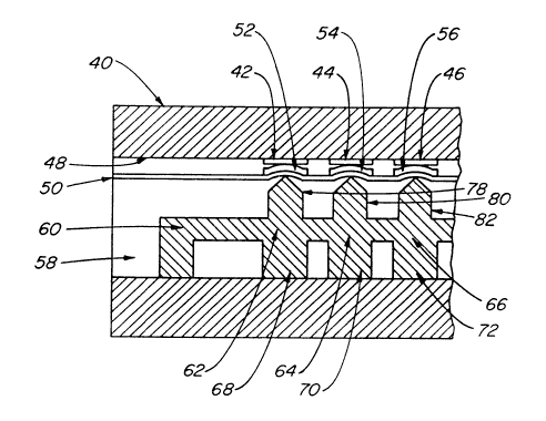
Re~erring now to Figure 3A, ther~ i8 ehown a
printhead 40, which may for ~xample be a thln ~ilm resistor
type printhsad having contact pAd~ 42, 44, and 46 on the
low~r ~urface therQo~ A flexible circuit memb~r 50 having
a conductive pattern thereon has been brought into alignm~nt
with the substratQ 40 as shown, with contact pads 52, 54 and
56 o~ th~ flex circuit pattern being aligned with the
contact pads 42, 44, and 46 on the printhead 40,
respectively
A near-linQar spring connect ~tructure i~ general-
ly de~ignat-d 5B and includ~ a horizontal central locating
member 60 and a plurality Or hollow xubber cylinders 62, 64
and 66 which extend therQthrough as ehown Th~ cylinders
62, 64 and 66 includ- lower cyllndrical Yections 68, 70 and
72 which extend downwardly and come to re~t on a rigid base
support member 76 The spring connect structurs 58 further
includo~ a plurality o~ upper, partially cylindrical and
partlally conical ~ctlons 78, 80 and 82 with conical tip~
which aro brought into alignment with the undQrsido o~ the
dimplec in tho fl~x circuit 50 ThiJ partially cyllndrical
and partially conical (tip) configuration 1~ better se~n in
tho enlargod isomQtric view of Figure 3B wherein th~
cylindrical ~tructura on the topsldQ o~ the central locating
member 60 is o~ solid con~tructlon and on the underside of
member 6Q i9 0~ hollow con~truction
Re~erring now to Flgure 4, a rubber cylinder ~uch
as cyl~nder 68 will undergo a sli~ht bulge a~ indicated when
force~ are applied vertically to the spring connect struc-
ture 58 to urge the flexible circuit 58 into electrical
contact with the contact pad~ 52, 54 and 56 on the printhead
Ideally, each succesQiva di~placed volu~- equals the
last, i e V0l - Vll - V21 - ~31 However, bscause the
walls o~ the cylinder 68 bulg~ lightly a~ indlcated, the
succes~ivQ volume displacement~ ar- not xactly gual, and
thl~ reactlon leads to a spring which 1~ nearly linear,
rather that praci~ely llnear Howovor, th~- cylindrical
shape i8 the most nearly line~r spring which can b- manu~ac-
tured at a minimum co~t and which yiolds tho near llnear
load ver~u~ di~tance curve in Figur- 2 Thi- spring connect
StrUCtUrQ 58 is capable of bringlng all pad- 52, 54 and 56
into contact with all corresponding contact pad- 42, 44 and
46 on the printhead 40 a~t-r applying a min$mum ~orco of
approximately LlI ~hown in Figure 2, a~ contrastQd to the
much greater ~orc- Ll ~or th~ nonlinear spring of the prior
art shown in FigurQ~ lA and lB.
Varlou! modirication~ may b- made to above des-
crib-d embodiment without departing ~rom tho ~cope o~ the
presont inventlon. For example, the cylindrical columns may
be either ~olid or hollow In addition, the present
invention i8 not limited to the lectrical connectlon o~
flQxibl- circuits to in~ ~et printheAds, but may be used for
the connectlon ot flex circults to other equivalent ~mall
7 ~ 3
geomQtry electroniC devices having small contact pads
thereon to which removable praqsure connections naed be
made.
Industrial Applicabili~y
The present lnventlon i8 used ~or the re~ovable
electrical connection o~ rlexiblo interconnect circuit~ to
ther~al ink ~et printhead~ or o~her small eloctronic device~
reguiring ouch ramovable connect~on. These printhead- are
used ~or controlling th- o~oction of ink ~ro~ a ther~l ink
~et print~r during a high spe~d printing operation.