Note: Descriptions are shown in the official language in which they were submitted.
APPARATUS COMPRISING A MONOLITHIC NONLINEAR FABRY-PEROT
ETALON, AND METHOD FOR P~ODUCING SAME
Field of the Invention
This invention pertains to the field of nonlinear optical
devices, and to apparatus incorporating such devices.
A detailed discussion of the prior art will be given
hereinbelow.
Definitions and Glossary of Terms
A material is herein said to be "optically nonlinear" at
a given frequency ~O if, over a spectral region that includes
vO, one or more parameters of the material, at substantially
constant temperature of the material, are dependent on the
intensity of the radiation incident on the material. Among
the parameters are the refractive index n and the absorptivity
~. This definition is intended to exclude changes in material
parameters that are due to heating caused by the incident
radiation. Nonlinear materials, to be of interest in this
application, typically have a nonlinearity greater than one-
tenth that GaAs and have material relaxation times shorter
than 10-8 sec.
A device herein is "optically nonlinear" if, for some
range of input intensity, at least one of the relevant
parameters of the device (e.g., transmissivity, reflectivity,
or absorptivity) changes with intensity. Nonlinear devices
contain at least one optically nonlinear material, also
referred to as an "active" material. A nonlinear device is
said to be refractive or absorptive, depending on whether the
predominant nonlinearity of the active material in the device
is in n or in ~, respectively. It is, of course, also
possible that n and ~ contribute approximately equally to the
nonlinearity.
Associated with nonlinear optical devices are at least
two "optical states", namely, a first state in ~hich one of
the relevant parameters of the device has a first value, and a
second state in which the relevant parameter has a second
value different from the first value. Exemplarily, the first
state may be a state of low transmissivity, and the second
,,~,
3'7'~
state a state of high transmissivity.
Summary of the Invention
We have discovered a method for fabricating a monolithic
nonlinear Fabry-Perot (FP) etalon, (i.e., a nonlinear etalon
both of whose mirrors are integral with the spacer, without
bonding layers and the like) that does not require etching
away a portion or all of the substrate material prior to
formation of one or both of the mirrors. The inventive method
thus is free of problems due to nonuniform etching that plague
the prior art. Other advantages of the invention will become
apparent.
The inventive method comprises providing an appropriate
substrate (e.g., GaAs, or some other semiconductor) having a
planar major surface, and depositing thereon in succession a
first multilayer mirror, a spacer layer, and a second
multilayer mirror. Deposition of the layers can be by any
appropriate process, e.g., molecular beam epitaxy (MBE) or
metalorganic chemical vapor deposition (MOCVD).
The basic method can be elaborated in various ways. For
instance, if it is desired to produce an etalon that can be
operated in a transmissive mode, then a compound substrate can
be provided, namely, a substrate comprising an appropriate
support structure (e.g. a GaAs wafer) with, e.g., a
transparent (at frequency vO) etch stop layer thereon. The
transparent layer not only protects the first mirror during
subsequent removal of all or a portion of the support
structure underneath one or more etalons, but also serves to
give mechanical support to the etalon(s). Of course, if a
suitable substrate that is transparent at vO is available, then
a transmission device can be produced even without deposition
of a transparent layer and etching away of the support
structure.
A further exemplary embodiment of the inventive method
comprises depositing an AlxGa1xAs (x > 0.5, e.g., 0.7) etch
stop layer onto a GaAs wafer, and depositing an etalon
according to the invention thereon. After completion of the
depositions all of the GaAs wafer is removed by known means,
,. ~
1~,93~9~
followed by complete removal of the etch stop layer, e.g. by
etching in concentrated HCl. The thus produced "flake"
(constituting one or more complete etalons) can be mounted on
or between appropriate support means, e.g., between two quartz
plates.
The inventive method can routinely produce nonlinear
etalons having high finesse (typically > lO, 20, or even 25),
and substantially uniform response over a relatively large
area (e.g., > lmm2), due to the ease with which high thickness
uniformity of the spacer (as well as the various mirror
layers) and low optical loss interfaces can be achieved. The
method is free of any critical etch step, i.e., of any etch
step that affects a material layer whose thickness and/or
thickness uniformity is critical to the optical quality of the
etalon. Furthermore, the inventive method results in
relatively rugged, mechanically and thermally stable etalons
whose manufacture does not require great manual dexterity; the
method lends itself to automation, and can be used to produce
multi "pixel" arrays by addition of known lithography and
etching (or ion implantation) steps to the inventive process.
Lastly, the inventive method is compatible with techniques
used in the manufacture of electronic and optoelectronic
devices. Thus, it is expected that it will be possible to
integrate nonlinear optical devices according to the invention
with electronic, optoelectronic, or perhaps other optical
devices on the same semiconductor chip.
In preferred embodiments, at least one of the two
multilayer mirrors of the nonlinear etalon is an "active"
mirror. An active mirror is a multilayer mirror in which at
least one of the materials forming the mirror shows
appropriate optical nonlinearity at vO, the operating frequency
of the device (thereby imparting nonlinearity to the mirror),
such that the mirror nonlinearity contributes to the nonlinear
behavior of the device. Exemplarily, an active mirror
consists of a multiplicity of AlAs and GaAs layers.
Devices according to the invention may comprise two or
more optical cavities in series, one or more optically linear
..
- .
1~37~
and/or nonlinear spacers, a transparent or opaque (at ~0)
support structure, etch stop layers, lattice matching layers,
reflection or antireflection layers, coating layers, and the
like. Although typically the optically active materials in
etalons according to the invention are crystalline, this is
not necessarily so.
Apparatus according to the invention typically comprises
a source of electromagnetic radiation of frequency ~0, at least
one nonlinear FP etalon according to the invention, means for
causing the vO radiation to interact with the etalon, whereby
the optical state of the etalon can be changed from a first to
a second state, and means that are responsive to the optical
state of the etalon. Exemplarily, such apparatus is an
optical computer are other optical data processing apparatus,
or is an optical communications apparatus.
Brief Descri~tion of the Drawings
FIGS. 1 and 2 schematically depict a prior art nonlinear
FP etalon;
FIG. 3 shows schematically a portion of a nonlinear FP
etalon according to the inventions;
FIGS. 4 and 5 each schematically show a portion of an
exemplary device comprising an array of nonlinear FP etalons
according to the invention;
FIG. 6 schematically depicts a portion of a monolithic
nonlinear FP etalon with mirror sidewalls that comprise a
"grating";
FIG. 7 schematically depicts a portion of a device
according to the invention comprising a nonlinear FP etalon,
grown on an opaque substrate, that is adapted for operation in
a transmissive mode; and
FIG. 8 schematically illustrates material properties
useful in the design of active mirrors.
Bistable and other nonlinear optical devices have been
known for some time, and a wide variety of signal processing
functions can be carried out by means of bistable devices.
"Bistable" and "nonlinear" are used herein interchangeably
unless indicated otherwise by the context. For instances,
3 r7 9 ~?~
U.S. Patent 4,012,699 discloses, inter alia, amplification of
a light beam by means of a cavity-enclosed positive-
temperature nonlinear medium. A recent monograph, H.M. Gibbs,
Optical Bistability: Controllina Liqht With Liqht, Academic
Press (1985) can serve as an introduction to the field and
discusses many of the possible modes of operation of bistable
optical devices. For instances, on pages 1-17, are given
brief discussions of bistable optical logic devices (both two-
state and many-state), of an optical transistor, of optical
discriminators, limiters, pulse compressors, oscillators,
gates, and flip-flops. Pages 195-239 contain a detailed
discussion of optical switching.
Many of the nonlinear optical devices comprise a
nonlinear FP etalon, a fixed-spacing optical cavity with an
optically nonlinear medium within the cavity. Furthermore,
much of the work on optically nonlinear devices has focused on
devices using solid, typically semiconductor, mostly
GaAs-based, nonlinear media. Such media are, for instance,
homogeneous GaAs, and GaAs-AlGaAs multiple quantum well (MQW)
structures.
As described for instance by J.L. Jewell et al, Materials
Letters, Vol. 1(5-6), pp. 148-151 (1983), GaAs-based nonlinear
FP etalons are fabricated by a rather difficult process. The
process exemplarily involves deposition of an about 3 ~m
GaAs-AlGaAs MQW structure on a GaAs substrate by molecular
beam epitaxy, and removal of the substrate by grinding and
selective etching so as to leave the MQW structure. The
resulting 3 ~m flake can then be mounted between dielectric
mirrors, thereby producing a nonlinear FP etalon.
FIGS. 1 and 2 schematically show another prior art FP
etalon formed by etching away a portion of a GaAs substrate.
See, H.M. Gibbs et al., Optics News, Vol. 5(3), pp. 6-12
(1979). The etalon 12 was produced by depositing a 0.2 ~m
Alo42Ga0s8As etch stop layer 15 onto the 150 ~m GaAs substrate
10, followed by deposition of the 4.1 ~m GaAs active spacer
layer 14 and of a further AlGaAs layer 15. After grinding and
etching away of the GaAs substrate in a 1 mm2 region ll of FIG.
~`~
3~
1, a (non-active) multilayer mirror 16 was formed by vapor
deposition on each layer 15.
Karpushko et al. (Journal of Applied Spectroscopy USSR,
Vol. 29, p. 1323 (1978)) disclosed an optical interference
filter comprising two mirrors with a ZnS spacer therebetween,
that exhibited optical bistability.
Prior art nonlinear etalons as described above have
significant shortcomings. Among these is the difficulty of
controlling the etching of the substrate sufficiently well to
achieve the high thickness uniformity required for high-
finesse mirrors. As is well known, if F is the desired
finesse associated with the etalon, then the thickness of the
spacer layer/etch stop layer combination has to be uniform to
at least ~ ~2nF over a significant portion of the flake, where
~ 0 is the vacuum wavelength of the operating radiation of the
device, and _ is the refractive index of the material. For
instance, if a finesse of 10 is desired, the spacer thickness
has to be constant to within about 11 nm for ~0 of about 0.87
~m. In etalons of the type described by Jewell et al. (op
cit), it is also difficult to achieve good and stable
mechanical and thermal contact between the flake and the
mirrors. Furthermore, the prior art methods for producing
nonlinear FP etalons tend to require substantial skill and
manual dexterity, and do not lend themselves to the formation
of multi-etalon arrays.
Due to the promise held by nonlinear FP etalons, for
instance, in the field of optical data processing, including
optical computing, and in optical communications, it would be
highly desirable to have available a method for producing such
etalons that are not subject to these and other shortcomings
of the prior art. This application discloses such a
technique. For information on optical computing, see
Proceedinqs of the IEEE, Vol. 72(7) 1984, especially A.A.
Sawchuck et al (pp. 758-779), and A. Huang (pp. 780-786).
A. Huang et al., Proceedinqs of the IEEE Global
Telecommunications Conference Atlanta, GA, 1984, pp. 121-125
discloses telecommunications apparatus that can be implemented
. . ~
. .
~a,
6a
using nonlinear optical devices according to the invention.
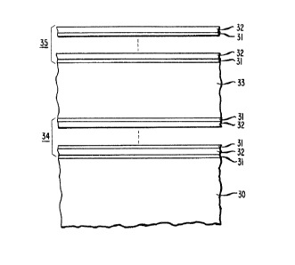
FIG. 3 shows schematically, in cross-section, a portion
of an exemplary monolithic FP etalon according to the
invention. It comprises a substrate 30, a first mirror 34, a
spacer 33, and a second mirror 35. The substrate typically is
an appropriate semiconductor wafer and the first mirror
comprises alternating layers 31 and 32 of two materials of
differing refractive index at v0.
The thickness of each type of layer depends, inter alia,
on the refractive index of the layer material and on vO.
Typically, the thickness of a layer is chosen to be ~O/4n. The
optical properties of periodically stratified media of the
type discussed herein are well known. See, for instance, M.
Born and E. Wolf, Principles of Optics, 2nd edition (1964),
pp. 66-70. Although generally it is advantageous to deposit
layers of constant thickness, it may at times be advantageous
to deposit tapered mirror layers, to provide frequency
tunability, or for other reasons.
The spacer 33 typically is approximately of thickness
~J2n (or a multiple thereof), and is of essentially uniform
thickness. It generally, but not necessarily, consists of
material that is optically active at vO. The second mirror
resembles the first mirror but need not comprise the same
combination of materials and/or contain the same number of
layers. One or both of the multilayer mirrors may (but need
not) comprise optically active material (at vO), as will be
discussed in more detail below.
Whereas FIG. 3 depicts an inventive etalon that is most
usefully employed in a reflective mode (unless substrate 30 is
transparent at vO), FIG. 7 shows schematically, in cross-
section, an exemplary inventive etalon that can be used in a
transmissive, as well as in a reflective mode. It differs
from the previously discussed etalon in comprising a compound
substrate 70 that comprises a layer 30 (e.g., GaAs of
appropriate thickness) and a transparent (at
t~
1~3~
v0) layer 71 thereon (e.g., 1-10~m of Alo 42Ga0 58As). As indicated in FIG. 7, aportion of 30 is removed, typically after completion of the deposition of the
etalon atop the compound substrate. Such removal can be by known means,
typically comprising lithography and etching (dry or wet), ion milling or the
5 like.
The inventive method for fabricating monolithic nonlinear FP etalons
comprises providing an appropriate substrate having a planar major surface,
and depositing thereon, by any appropriate technique, or combination of
techniques, the first mirror, the spacer, and the second mirror, as well as
10 possibly other layers. Advantageously, the sequence of depositions is carried out
without intermittent handling of the wafer, e.g., in an MBE chamber with
multiple sources.
Following completion of the etalon deposition further manufacturing
steps may be carried out. Exemplarily, these steps may include deposition of a
15 protective coating onto the top mirror, or coating of the top (and/or bottom)surface of the thus produced combination with an appropriate resist, such that
the top (and/or bottom) surface of the combination can then be patterned by
methods well known in the semiconductor industry. By means of such
patterning, an array of FP etalons can be produced. Such an array can easily
20 contain 100x100 etalons, and may be as large as 1000x1000. It is considered to
be one of the main advantages of the inventive method that it permits relativelyeasy formation of such arrays.
FIG. 4 schematically depicts a portion of a device 40 according to the
invention comprising an array of reflective OR logic elements. On the common
25 substrate 30 are formed a multiplicity of individual, optically isolated mesa-like
elements 41 of the type depicted in FIG. 3. By "optically isolated", we mean
herein that a change in the optical state of any one of the elements does not
have a substantial effect on the optical state of any of the other elements of the
array.
Exemplarily, the elements 41 can be operated as follows: A probe
beam 42 (of frequency vp, with vp selected such that the nonlinearity of the
etalons is relatively small at vp), can be directed onto one or more of the
elements, resulting in substantially no reflected probe radiation 42'. When bothan "input" beam 43 (of frequency v0, with v0 selected such that the nonlinearity
1~3~7~L~
of the etalons is relatively large at vO) and the probe beam 42 are directed onto
an etalon, the optical state of the etalon can change such that a substantial
amount of probe radiation 42'is reflected. For instance, if the etalon contains a
GaAs spacer, then ~O and vp exemplarily are 868 and 873 nm, respectively. If
5 other nonlinear materials (e.g., InSb, InGaAsP and related compounds) are
used, then the appropriate frequencies typically will be different.
The presence of 42' can be detected by known means (e.g., a filter and a
photodetector), thereby providing a read-out indicative of the optical state of
the element. If two or more input beams 43 can be directed onto an element,
10 each of which can cause the described change in the optical state of the
element, then the element functions as a logical OR gate. Other logic functions
can, of course, also be implemented.
FIG. 5 schematically shows another exemplary array of FP etalons
according to the invention. In this embodiment, the optical isolation between
15 etalons 33 is achieved not be removal of material as shown in FIG. 4, but by
changing the optical properties of the material in regions 51. For instance, thenonlinear properties in regions 51 can be changed by ion implantation (e.g., by
proton implantation), such that adjacent etalons are effectively decoupled.
FIG. 6 schematically depicts a portion of an exemplary etalon according
to the invention. Etalon 41 has one or more side surfaces that intersect the
layers of the second mirror, the intersected mirror layers forming a "grating",
i.e., a periodic variation in the surface topography of the intersecting surface.
Such a grating can easily be produced, e.g., by contacting the side surfaces with
an etching medium in which the etch rates of the two mirror materials are
25 different. The presence of an appropriately formed grating may increase the
operational efficiency of etalons according to the invention. However, the effect
of a grating on the Gperation of an etalon can be expected to depend on the
details of the situation. Thus, minor experimentation may be required, for
instance, to determine which of the two layer materials should be etched more
30 rapidly. Although FIG. 6 shows a second mirror only, it will be understood that
the first mirror can be similarly treated.
FIG. 8 illustrates some material properties that can advantageously be
used in the design and manufacture of active mirrors according to the invention.The figure schematically depicts curves of mirror reflectivity as a function of
1?.~3~7~
wavelength. Curve 80 represents the reflectivity of an active mirror measured
at such low incident intensity that the effect of nonlinearity is negligible. Ascan be seen, the reflectivity is maximum at a frequency vj~v0. If the
nonlinearity of the mirror is essentially dispersive, and if the reflectivity is5 measured with incident radiation of intensity greater than some threshold
intensity It (to be defined below), then curve 81, with maximum at some
frequency v0, results. On the other hand, if the mirror nonlinearity is
essentially absorptive, then, for intensity >It, curve 82 (with maximum
reflectivity greater than that of 80 and substantially at v;) results. Lastly, if the
10 mirror nonlinearity is both dispersive and absorptive, curve 83, with maximumreflectivity greater than 80 (or 81) and at some frequency 7~Vj (e.g., at vO)
results. Thus, the reflectivity of an active mirror at a given frequency can vary
substantially as a function of intensity. In the high intensity state, it can beeither larger (as at v0 of FIG. 8) or smaller (as at v;) than in the low intensity
15 state. Both of these possibilities are considered to be potentially useful.
Preferred inventive nonlinear FP etalons with active mirrors thus can be
designed such that in a first optical state, the reflectivity of at least one of the
mirrors of the etalon has a maximum at v;~vO, and that in a second optical
state, the mirror has maximum reflectivity at v0. The threshold intensity It is
20 an intensity of radiation of frequency v0 that is associated with the change of
the state of the etalon from the first to the second optical state.
Example I. A 500,um thick, (100) cut, 2-inch diameter GaAs wafer was,
after cleaning by a known technique, mounted in the specimen holder of a
multi-source MBE system, and a relatively thin (~ l~m) GaAs smoothing layer
25 deposited thereon. Onto the thus prepared (100) surface of the substrate wafer
were deposited ~-1/2 pairs of AlAs/GaAs layers, of thickness 72.3 nm and
63.5 nm respectively. Deposition of the last AlAs iayer was followed by
deposition of a nonlinear spacer, namely, an essentially uniform thickness
(~ 2,um) layer of GaAs. This, in turn, was followed by deposition of 7 pairs of
30 AlAs/GaAs layers, also of 72.3 and 63.5 nm thickness, respectively, with the last
layer being GaAs. The thus manufactured nonlinear etalon had a measured
finesse of about 15 for radiation of (vacuum) wavelength 880 nm.
3~
- 10 -
Example II. A first active mirror, a spacer layer, and a second active
mirror are deposited substantially as described in Example I. A patterned resistlayer is formed atop the second mirror, the resist layer containing a 100 x 100
array of 2~m x 2,um resist patches on 4~m centers. The wafer is dry etched by
5 a known process, resulting in removal of essentially all of the deposited material
not protected by resist, thereby producing a 100x100 array of optically isolatednonlinear FP etalons adapted for operation at ~o=873 nm as reflective NOR
gates, with the probe beam wavelength being about 880 nm.
Example III. An array of nonlinear FP etalons adapted for operation at
10 873 nm in a transmissive, or reflective and transmissive, mode is manufactured
substantially as described in Example II, except that, prior to deposition of the
first mirror, an Alo 42GaO 5~As layer of appropriate thickness (~2~m) is
deposited onto the GaAs wafer, etching of the deposited material is stopped at
the AlGaAs layer, and the GaAs wafer is etched to the AlGaAs layer in the
15 region opposite the etalon array.