Note: Descriptions are shown in the official language in which they were submitted.
r~
-1- RCA 82,603
GROUNDING ARRANGEMENT USEFUL IN A DISPLAY APPARATUS
The present invent on concerns a grounding
arrangement which is particularly useful in a display
system such as a television receiver, monitor or similar
apparatus.
Modern display systems such as television
receivers and monitors offer a large number of user
features usually requixing control units which are
connected to almost all of the major signal processing
units such as the tuner, video, audio and deflection units.
In such arrangements, care should be taken in arranging the
extensive reference potential or ground paths to inhibit
unwanted currents and voltages, which may adversely affect
the operation of the display system, from being developed
in the reference potential or ground paths due to the
operation of the signal processing units.
An aspect of the present invention concerns the
recognition that the magnetic fields produced by the
deflection unit of a display system can induce large
currents in closed loop reference potential or ground paths
which in turn can cause disturbances of the reference
potentials with respect to which signals are processed in
various portions of the display system.
In a preferred embodiment of the present
invention, a control system having first and second
interconnected control units for controlling different
signal processing portions of an apparatus such as a
television receiver or monitor is provided with first and
second unconnected reference potential input points for
receiving a reference potential from different points of a
reference potential (e.g., ground) bus so as to form a
reference potential distri~ution arrangement without a
continuous, closed loop subject to magnetically induced
currents such as may be produced by a deflection unit. A
threshold responsive gate is coupled between the reference
potential input points of the first and second control
units for selectively connecting or clamping them together
when the potential difference hetween them exceeds a
.f~ 9
-~- RCA 82,603
threshold to inhibit excessively large and possibly
damaging potential differences from being developed, e.g.,
due to high voltage discharges of an associated display
tube.
By way of example, the invention will be
explained with respect to the accompanying Drawing in
which:
FIGURE 1 shows partly in block form and partly in
schematic form a television receiver incorporating the
preferred embodiment of the invention; and
FIGURE lA shows in schematic form a modification
to the preferred embodiment of the invention shown in
FIGURE 1.
In the Drawing, multiconductor signal paths are
indicated by double lines.
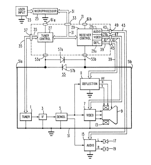
The television receiver shown in FIGURE 1
includes a tuner 1 for tuning the RF television signal
corresponding to a selected channel to form a corresponding
IF signal. The IF signal is filtered by an IF filter 3 and
demodulated by a demodulator 5 to produce baseband
composite video and audio signals. The composite video
signal is coupled to a video processing unit 7 which
processes the luminance and chrominance components of the
video signal to produce red tR), green (G) and blue (B)
drive signals for respective electron guns of a picture
tube 9. The video signal is also coupled to a deflection
processing unit 11 which processes the synchronization
components of the video signal to produce horizontal (H)
- and vertical (V) deflection signals which are coupled to
deflection coils 13 associated with picture tube 9 for
deflecting the electron beams produced by the electron guns
of picture tube 9. Operating voltages for the receiver
including a high voltage (HV) for picture tube 9 are also
developed by deflection processing unit 11. The audio
signals produced by demodulator 5 are coupled to an audio
processing unit 15 which provides left ~L) and right ~R)
stereo signals to speakers 17 and 19.
1~33`7~9
-3- RCA 82,603
Various functions of the receiver performed by
the processing units so far described are controlled by a
control unit 21 in response to user commands provided by
means of a user input unit 23 and communicated to control
unit 21 by a microprocessor 25. User input unit 23 may
comprise a keyboard mounted on the receiver itself or on a
remote control transmitter coupled through an infra-red or
ultrasonic link to the receiver. The commands from user
input unit 23 are in the form of digitally encoded signals
and microprocessor 25 decodes these encoded signals and
generates further digitally encoded signals for control
unit 21 which generates the actual control signals for
controlling the various processing units.
Control unit 21 desirably is incorporated in a
single integrated circuit (indicated by the dashed line),
e.g., utilizing CMOS technology, which is partitioned into
a first control unit 27 for controlling tuner 1 and a
second control unit 29 for controlling other processing
units of the receiver including video processing unit 7,
deflection processing unit 11 and audio processing unit 15.
The reasons for the partitioning will be e~plained below.
Microprocessor 25 is coupled to first-or tuner control unit
27 and to second or receiver control unit 29 through a data
bus 31, the conductors of which are connected to respective
terminals (generally indicated by a rectangle 33) of
control unit 21. Tuner control unit 27 and receiver
control unit 29 are electrically interconnected by data bus
31.
Tuner control unit 27 generates a tuning control
signal and bandswitching signals for tuner 1 to tune a
selected one of the plurality of RF televisiGn signals
being received corresponding to respective channels. Tuner
control unit 27 is coupled to tuner 1 through a control bus
35, the conductors of which are connected to respective
terminals (generally indicated by a rectangle 37) of
control unit 21. Tuner control unit 27 may comprise a
frequency synthesizer or phase locked loop described, e.g.,
in U. S. patent 4,405,947 issued in the name of J. Tults
7~
-4- RCA 82,603
and M. P. French on September 20, 1983. A phase locked
loop receives a frequency divided version of the local
oscillator signal generated within the tuner (and therefore
control bus 35 between tuner control unit 27 and tuner 1
h`as an arrow at both ends) and compares it with a reference
frequency signal to generate frequency error pulses, the
amplitude and duration of which represent the deviation
between the actual frequency of the local oscillator signal
and the desired frequency. These error pulses are filtered
by a lowpass filter to generate a tuning voltage for the
local oscillator. Since control unit 21 uses primarily
digital components, the lowpass filter required for a phase
locked loop is desirably located in tuner 1.
Receiver control unit 29 is partitioned into
deflection, video and audio control portions 29a, 29b and
29c for generating control signals for deflection, video
and audio signal processing units 11, 7 and 15,
respectively. Deflection, video and audio control units
29a, 29b and 29c are coupled to deflection, video and audio
processing units 11, 7 and 15 by respective control buses
39, 41 and 43 and terminals (generally indicated by
rectangles 45, 47 and 49) of control unit 21.
By way of example of the various functions
controlled by receiver control unit 29, deflection control
portion 29a generates "receiver on" and "receiver off"
control signals for causing deflection processing unit 11
to provide or not provide operating voltages for various
portions of the receiver. For this purpose, deflection
control portion 29a may include a flip-flop which is set
and reset in response to user initiated commands from user
input 23 and coupled to control unit 21 by way of
microprocessor 25 and data bus 31.
Video control portion 29b generates control
signals for controlling the brightness and contrast
produced by picture tube 9. For this purpose, video
control portion 29b may include digital-to-analog
converters (DACs) for generating control voltages for the
brightness and contrast functions in response to user
1;~93';"~9
-5- RCA 82,603
initiated command signals. Since control unit 29 primarily
includes digital components, the filters for the DACs are
desirably included in video processing unit 7. Video
control unit 29c may also provide character representative
control signals to video processing unit 7 for causing
alphanumeric or other graphic material to be displayed,
e.g., for indicating the selected channel number and/or the
time of day. For this purpose, video processing unit 29
may include a character generator of the type described in
U. S. patent 3,984,828 issued in the name of B. W. Beyers,
on October 5, 1976. As a further example, video control
portion 29b may generate a control signal for controlling a
switching unit within video processing unit 7 for selecting
either the red, green and blue signals produced in response
to the video signal supplied by demodulator 5 or red, green
and blue signals provided by an external source such as a
home computer or video game.
Audio control portion 29c may include a DAC for
controlling the volume level. It may also generate a
control signal for selecting either monophonic or
stereophonic sound reproduction.
U. S. patent 4,249,089 issued in the names of
J. J. Wolford and J. B. George on February 3, 1981
discloses the arrangement of an integrated circuit with
provision including a flip-flop and a DAC for controlling
the on/off state and volume level, respectively, of a
television receiver. Similar DAC arrangements can be used
for controlling brightness and contrast.
Television receivers of the CTC-131 chassis type
manufactured by RCA Corporation, Indianapolis, Indiana and
described in RCA Color Television Basic Service Data file
1984, CTC 131 Second Edition provide similar and additional
control function.
The various information signal voltages processed
in tuner 1, IF unit 3, demodulator 5, video processing unit
7, deflection processing unit ll and audio processing unit
15 and the various control signal voltages generated by
control unit 21 (as well as the command and data signal
1~93 ~
~6- RCA 82,603
voltages processed by user input unit 23 and microprocessor
25) are referenced to a common reference potential, e.g.,
ground as shown in FIGURE 1. The ground reference
potential is distributed by a ground reference potential
bus 51 comprising, e.g., a series of conductors connected
between the various reference potential input points of
information signal processing units 1, 3, 5, 7, 11, 15 and
control related units 21, 23 and 25~
Assuming for the moment that bus 51 formed a
continuous, closed loop (with separate ground reference
potential input terminals 53a and 53b, to be discussed
below, replaced by a single terminal) of significant area,
then ground bus 51 would be capable of conducting
potentially large currents induced in it due to the
magnetic fields generated by deflection processing unit 11
and associated deflection coils 13. Since ground bus 51 is
typically long, it exhibits relatively large impedances
between reference potential input points of the units to
which it is connected. As a result, the magnetically
induced currents can cause relatively large and variable
voltage drops to be developed between the reference
potential input points which may adversely affect the
operation of the television receiver. For example, such
voltage drops in grounding systems have been found to
produce noise and beats in the reproduced picture and audio
responses. Therefore it is desirable to avoid the use of a
continuous, closed loop reference potential of any
appreciable area.
One solution would be to ensure that control unit
21 was connected to the ground by only one conductor rather
than in the manner shown in FIGURE 1 by which control unit
21 is connected to ground by both of bus segments 51a and
51b thereby avoiding the formation of a continuous, closed
loop ground path. However, it was found that certain
control signals are particularly susceptible to ground
disturbances necessitating the loop configuration of ground
bus 51. By way of example, it has been found that the
tuning error control pulses generated by a phase locked
;3'7'3~
-7- RCA 82,603
loop which may be included in tuner control unit 27 and the
character signals generated by a character generator which
may be included in video control portion 29b of receiver
control unit 29 are particularly susceptible to ground
potential disturbances. Even in the absence of a
continuous, closed loop ground path, ground disturbances
can be caused in normal operation due to the flow of
return currents from the processing units and radiation.
Accordingly, it is desirable to connect the ground terminal
of control unit 21 to tuner 1 and video processing unit 7
by bus segments 51a and 51b (thereby forming a continuous,
closed ground loop) to reduce the ground disturbances due
to normal return currents.
In the present grounding arrangement shown in
FIGURE 1, the otherwise continuous closed ground formed by
ground bus 51 is broken by partitioning the control unit 21
into first and second control units 27 and 29 and providing
separate respective reference potential input terminals 53a
and 53b for each of first and second control units 27 and
29 rather than a single referen~e potential input terminal
for all of control unit 21. Reference potential input
terminal 53a is connected via bus segment 51a to the
reference potential input of tuner 1 and reference
potential input terminal 53b is connected via bus segment
51b to the reference potential input of video processing
unit 7. Since reference potential input terminals 53a and
53b are not connected, a continuous, closed ground loop
subject to the conduction of currents induced from magnetic
fields is not formed.
While reference potential terminals 53a and 53b
are not directly connected together, a threshold responsive
gating circuit 55 is coupled b~tween them to selectively
connect them together for conduction and thereby clamp the
voltage at one to the other when the voltage between them
exceeds a predetermined threshold. The purpose of gating
or clamping circuit 55 is to prevent the voltage between
potential input terminals 53a and 53b from exceeding a safe
limit. Without gating circuit 55, current surges through
'7~9
-8- RCA 82,603
ground bus 51 due to high energy discharges to ground
associated with picture tube 9 may cause excessively large
voltages to be developed between terminals 53a and 53b.
Since the semiconductor circuits of tuner control unit 27
and of receiver control unit 29 are interconnected by the
conductors of data bus 31, the excessively large voltages
developed between terminals could be coupled across various
semiconductor circuits within units 27 and 29 thereby
subjecting them to damage. This is inhibited by gating
circuit 55. A bi-directional gating circuit is utilized
since the discharges are unpredictable and therefore the
polarity of the excessive voltages cannot be predicted.
As shown in FIGURE 1, gating circuit 55 includes
diodes 57a and 57b connected in parallel between terminals
53a and 53b and poled in opposite senses. In this case,
the threshold and clamping voltages are the same in both
senses (directions of conduction), e.g., about 0.7 volts.
It will be appreciated that diodes 57a and 57b could
comprise the base-emitter junctions of bipolar transistors,
with the respective collector and base electrodes connected
together.
Other gating circuit configurations are possible.
As one example, as shown in FIGURE lA, a Zener diode 59 may
be employed. In this case, the threshold and clamping
voltage in one sense (direction of conduction) is different
than in the other sense. That is, if the voltage at
terminal 53a exceeds the voltage at terminal 53b, the
threshold and clamping voltage is the Zener or reverse
conduction voltage of Zener diode 59; and if the voltage at
terminal 53b exceeds the voltage at terminal 53a, the
threshold and clamping voltage is the forward conduction
voltage of Zener diode 59, e.g., about 0.7 volts.
Desirably, the Zener voltage is selected to be near as
possible, e.g., about 1.2 volts, to the forward voltage.
The Zener diode avoids the need for two inventory devices
but may in fact be more expensive. A Zener diode also
tends to act more slowly than a normal diode.
Whatever specific gating circuitry is utili~ed,
the theshold voltage should exceed the highest expected
lZ93~7~9
-9- RCA 82,603
potential between terminals 53a and 53b due to normal
operation of the television receiver to ensure that
terminals 53a and 53b are not normally electrically
connected for conduction currents between them (i.e., that
gate 55 is not normally conductive).
To prevent interference between control units 27
and 29 through the power supply path, control unit 21 is
provided with separate power supply terminals 61a and 61b
for control unit 27 and 29, respectively. Terminals 61a
and 61b are desirably bypassed to ground to prevent
radiation from control unit by respective bypass capacitors
(not shown). If desired, a filter such as a series L-C
filter, may be connected between power supply terminals 61a
and 61b to enhance the isolation between control units 27
and 29.
While the invention has been described in terms
of specific embodiments, the following claims are intended
to cover modifications. For example, gating circuits which
have different threshold and clamping voltages may be used.