Note: Descriptions are shown in the official language in which they were submitted.
r~
~ 1 ~
This invention relates to automotive sound
systems, and particularly to a system which employs
psychoacoustic contouring of the program material
signal, based upon the hearing characteristics o~ the
human ear.
It has long been known that the apparent
sensitivity of the human ear is dependent upon how loud
program material is, and the frequency of that program
material. For example, it is known that, at low program
10 material loudness levels, low frequency program material
is much lower in apparent volume than a higher frequency
program material. As loudness level increases, the
apparent difference in loudness between e~ual amplitude
low frequency program material signals and high
15 frequency program material signals diminishes. This
effect is described in various reference works under the
heading "equal loudness contours." Equalization loosely
based upon equal loudness contours has been utilized in
the past.
Invariably/ in the design of an audio system
for an automotive vehicle, certain compromises are
made. The acoustic environment of an automohile is a
unique environment. It is small, fully enclosed and
relatively noisy. There are surfaces in the vehicle
that are highly absorptive, such as car seats, padded
dashboards and headliners. There are surfaces in a car
that are highly reflective, such as window glass. There
are size and placement constraints on the choice of
loudspeakers to play within the environment of an
automobile.
3~3~
Certain design advantages, however, are
available in the au~omotive sound system environment.
For example, the designer knows generally where the
occupants of the car are going to be seated. Therefore,
specific equalization of a system at the intended
location of the listener's ear can be achieved. The
relatively small enclosed space of an automobile
interior can be used to good advantage in terms of
bandwidth with proper system design.
One demand for a high~quality automotive sound
system is that the bandwidth of the system be as wide as
possible. Much musical information otherwise can be
masked or lost in a system that is "midrange-heavy," has
acoustic dips or "notches", or does not reproduce high
or low frequencies with maximum fidelity.
To deal with the sound absorption
characteristics of an automobile interior, it is
essential when designing an automotive sound system to
address the true sound power generated by the speakers
mounted in the automobile. Since speakers generally
become more directional as frequency of program material
increases, the sound power radiated as frequency
increases is radiated in a narrower and narrower beam.
The contributions of off-axis sound pressure response
become more and more critical as speaker mounting
location considerations restrict the ideal placement of
speakers.
According to the invention, a sound system
comprises a channel having a low level input for
coupling to a source of program material, multiple,
_3~ 3~
independently selectable means providing equalization poles,
means including an input stage for independently and
selectively coupling one or more of the multiple equalization
pole-providing means to the low level input, an amplifier,
means for coupling the selected one or more of the multiple
equaliæation pole-providing means to the amplifier, a
tLansducer, and means for coupling the transducer to the
amplifier, the means for coupling the selected one or more of
the multiple equalization pole-providing means to the amplifier
comprising a ~ilter having a variable lower corner frequency
and a control input terminal, the system further comprising a
low-pass filter circuit for generating a feedback signal, means
for coupling the low-pass filter circuit to the amplifier, and
means for coupling the low-pass filter circuit to the control
input terminal of the variable corner frequenc~ filter.
Stated another way, a sound system comprises at least
one channel, each such channel having a low level input for
coupling to a source of program material, multiple,
independently selectable means providing equalization poles,
means for independently and selectively coupling one or more of
the multiple equalization pole-providing means to -the low level
input, an amplifier, means comprising a filter having a
variable lower corner frequency and a control input terminal
for coupling the selected one or more of the multiple
equalization pole-providing means to the amplifier, a
transducer, means for coupling the transducer to the amplifier,
a low-pass filter circuit for generating a feedback signal,
means for coupling the low-pass filter circuit to the
amplifier, and means for coupling the low-pass filter circuit
to the control input terminal of the variable corner frequency
filter.
.i
3~3~
-3a-
Stated in yet another way, a sound system comprises at
least two channels, each including means for coupling a source
of program material to the channel, an input stage, a second
stage, multiple, independently selectable mea~s providing
equalization poles, means for independently and selectively
coupling one or more of the multiple equalization
pole-providing means to the input stage and to the second
stage, a filter having a variable lower corner frequency and a
control input terminal, means for coupling the second stage to
the variable corner frequency filter, an amplifier, means for
coupling the variable corner frequency filter to the amplifier,
a transducer, means for coupling the transducer to the
amplifier, a low-pass filter circuit for generating a eedback
signal, means for coupling the low-pass filter circuit to the
amplifier, and means for coupling the low-pass filter circuit
to the control input terminal of the variable corner frequency
filter, the low-pass filter circuit controlling the variable
lower corner frequency.
Illustratively, according to the invention, there are
four such channels divided into two pairs and the low-pass
filter circuits in one pair of such channels have higher corner
frequencies than the low-pass filter circuits in the other pair
of such channels.
Additionall~, illustrativel~, the sound system is an
automotive sound system, the two pairs of channels
5614p
333~33~
comprise a pair of front channels and a pair of rear
channels and the low-pass filter circuits in the rear
channels have relatively lower corner frequencies than
the low-pass filter circuits in the front channels.
This provides a preferred technique for
equalizing the sound system to a listening area, such as
the interior of an automotive vehicle. This permits
"tailoring" of the equalization characteristics of the
means which couple the program material source to the
discriminating means to the interior of a particular
automotive vehicle.
The system of the present inYention uses
woofers for extended low frequency performance, midrange
speakers for smooth, low distortion midband output, and
tweeters for extended high frequency performance. The
system comprises ~our three-way speaker systems, one in
each corner of the automotive vehicle interior. The
radiating area of the woofers is adequate to provide
reduced woofer excursion necessary for a particular
sound pressure level (SPL). Thus, distortion is
reduced. The use of midrange speakers permits the power
response characteristic of the sound system to remain
much flatter to a higher frequency than prior art
systems. The midrange speakers have smaller diaphragms
with wider directional patterns in the mid-band
frequencies. Positioning of the speakers of the system
thus becomes less critical for proper tonal balance than
was the case with prior art systems. The large piston
area of the woofers of the described system at low
frequency produces high output with low coil excursion.
3~33~
The reduced coil excursion leads to lower distortion at
the same output levels as prior art higher-excursion
transducers. The excursion of the midrange speakers of
the present described system is also very low, because
the midrange speakers are crossed over at 400 Hz, where
cone excursion is somewhat lower. The woofers and
midrange speakers of the described sound system are
separate from each other (discreet). Therefore,
distortion due to modulation by a low frequency piston
motion is reduced in the described system, as compared
to a single, full-range driver.
The sound system described in this application
makes considerable use of psychoacoustic e~fects. The
performance of this system is such that full frequency
range reproduction is provided without having to adjust
the system playback level to the level of the original
performance. Equalizing to the contours utilized in the
described system provides an added benefit. Low
frequency sounds in an automotive vehicle environment
are usually masked by road and engine noise. In order
to hear low frequency sounds in prior art automotive
sound systems, especially at low listening levels,
considerable bass boost was needed. With the system of
the present invention, the correct amount of bass boost
is added so that the frequency spectrum is properly
balanced at all volume levels. The system automatically
makes the needed bass frequency adjustment, depending
upon the voltage at the loudspeaker voice coils, so that
bass performance is maximized.
An additional benefit of this contouring action
is that it is virtually impossible to overdrive the
33~3~
system's speakers. The same circuitry that maximizes
the bass performance at low program matexial amplitudes
minimizes the likelihood o e~ceeding the system's power
handling capability at high program material
amplitudes. This provides a means of achieving
essentially full system output capability at all levels
by employing circuitry which amounts to an analog
excursion control computer. The analog excursion
control computer permits the highest possible output
down to the lowest possible frequency regardless of the
program material playback level. This circuitry is
always active in the system and provides the widest
possible bandwidth and proper low frequency tonal
balance for every listening level. Moreover, distortion
due to excessive driver excursion is eliminated by this
circuitry.
It is envisioned that the automotive sound
system here described will make use of all available
package space to ma~imize low fre~uency performan~e
capability. For example, it is envisioned that the rear
speakers for both channels (RR and LR) will be mounted
on the automobile package tray or behind the rear seat
of the automobile so that they work into the trunk
volume. Illustratively, trunk volume might be 60 to 300
liters. This is much larger than the customary prior
art mounting in which the rear seat speakers work into
an enclosure having a volume on the order of 3 liters.
This eliminates the need for the rear seat speakers,
particularly the woofers, to have additional electrical
amplification to overcome any rolloff deficiencies
3~
created by a small enclosure. The essentially infinite
baffle provided by the trunk volume results in
substantial low frequency output, permitting appreciable
e~cursion in the piston range at frequencies below 50 Hz.
The circuitry o the present invention provides
substantially constant excursion in the 20 Hz through 50
Hz range. In this fre~uency range, the passenger
compartment becomes pressurized at a uniform pressure,
based on equal piston displacement, such that the
response measures flat through this frequency range.
This phenomenon would not occur in free space, because
radiation resistance in free space decreases with
decreasing frequency, and a 12 dB per octave drop with
increasing frequency would be observed. However, in an
essentially sealed space, such as the automctive vehicle
interior, the piston motion creates a uniform pressure
differential between the vehicle interior listening
space and the outside. With open windows, doors and
sunroofs, the radiation loads are generally favorable,
such that the system will still measure substantially
flat, even though no sealed space e~ists. A vented
system, such as some of the prior art high fidelity
sound systems proposed for automotive vehicles, cannot
achieve this same effect because the venting provides a
"leak" for the low frequency output of the transducers.
In such prior art systems, transducer movement at these
frequencies in the piston range is cancelled by the back
wave arriving through the port or vent out of phase with
the front wave. The vent, which is used to achieve 3 dB
greater output at 50 Hz, is employed at the sacrifice of
a 24 dB per octave rolloff below 50 Hz.
1~3~3~
The distribution of sound throughout the
automotive vehicle interior listening ~pace is as
important as smooth frequency response and wide
bandwidth to the overall sound quality within the
listening space. An e~ample of a sound system
constructed according to the present invention ~mploys
four midrange speakers of equal bandwidth and tonal
qualities, one in each corner of the vehicle interior.
The result is a tonal characteristic that is even and
balanced from right to left and from front to rear of
the listening space. Th~ desired quality of tonal
ba~ance is not lost when the system if faded from front
to rear. To enhance the low frequency performance of
the system, circular 5-1/4" (13.34 cm.) front channel
woofers are augmented below 100 Hz by the rear eliptical
6" x 9" (15.24 cm. x 22.86 cm.) woofers when the system
is faded forward. Additionally, in any automotive
vehicle in which the installation of the sound system of
the present invention is restricted to midrange speakers
in the front channels, because of size restraints, for
example, the benefit of augmented low frequency
information from the rear channels is available with the
system of the present invention. Since the system is
operating in the pressure mode, as described above, the
directionality of the low frequency information is
undetectable. Frequency selective fading, in which the
higher frequencies are faded front-to-rear or
rear-to-front by the fade control, but the low
frequencies are distributed evenly throughout the
listening space, enhances the tonal balance of the
system.
:~L29393~
The circuitry of the present invention provides
a regulated DC-to-DC converter circuit that converts the
vehicle's nominal ~14 ~DC to +28 VDC, ~15 VDC, -15 VD~
and -28 VDC for the power amplifiers and analog bass
computers. The converter-type amplifier is used because
of its excellent regulating characteristics and its very
high voltage swing to permit sufficient drive voltage
into a 4 ohm speaker network. The dynamic range
requirement of the sound system of the present invention
demands a relatively strong and stable power supply,
permitting peak currents of over 30 amperes. The supply
of the present invention, which is a switching power
supply, employs a 50 KHz push-pull oscillator and a
shielded 1:2 voltage transformer.
The input stags of the circuitry of the sound
system of this invention uses a differential input for
maximum rejection of radiated noise from other vehicle
circuits such as the alternator, ignition and other
electrical devices within the vehicle. Isolated input,
output and chassis grounds afford added noise immunity.
The circuit includes integral short circuit protection,
as well as low voltage and thermal shutdown. A
completely buffered equalization circuit provides
versatile parametric equalization for each of the four
audio channels. The equalization circuits are
custom-adjusted for the particular vehicle in which the
sound system is being installed.
The bass contour control of the present
invention is, in effect, an analog excursion control
computer which senses the voltage at the speaker voice
3l~9~33:~
-- 10 --
coil and controls that voltage relative to sound
pressure in the vehicle passenger compartment according
to a preprogrammed set of instructions. The frequency
response is balanced to approximate the equal loudness
contours. The level corresponding to approximately 100
dB measures flat, while the level at 60 dB has 20 to 25
dB relative bass boost. Separate bass contour control
circuits, or analog e~cursion control computers, are
provided for the front and rear channels. The front and
rear circuits have different circuit constants to match
the characteristics of the front or rear speakers, and
their respective environments. These bass contour
control circuits are adjustable, and can be be fine
tuned to accommodate different speakers in each location.
The power amplifier for each channel is
designed to operate into a 4 ohm speaker load.
The system provides a steady state sound
pressure level capability of 105 dB, in a frequency
range of 40 Hz - 200 KHz for each channel with less than
10% total harmonic distortion, and 95 dB with less than
5% total harmonic distortion between 200 Hz and 20 KHz.
The system is equalized to +/- 4 dB from the baseline
contour for 95 percent of occupants in the driver's
seat. Each channel's power amplifier is capable of
providing 35 watts of power, when all channels are
driven, with less than .07% distortion. The
loudspeakers are matched to typically +/-2 dB through
the operating range, measured on axis, referenced to
wide band pink noise averaged for 32 seconds. Crossover
frequencies between woofers and midrange speakers are
~3~33
400 Hz, and between midrange speakers and tweeters are 7
KHz.
Each rear channel's speaker complement includes
a 6" ~ 9" (15.24 cm. x 22.86 cm.) woofer, two 3-1/2"
(8.89 cm.) midrange speakers and two 1/2" ~1.27 cm.)
dome tweeters. Each front channel's speaker complement
includes a 5-1/4" (13.34 cm.) woofer, two 3~1~2" (~.89
cm.) midrange speakers and two 1/2" (1.27 cm.) dome
tweeters. The rear woofers have 16 oz. (454 gram)
barium errite magnets. A11 woofers have Symmetric
Field Geometry motor configurations. 1-1/2" (3.81 cm.)
voice coils provide long linear excursions for the rear
woofers. The woofer voice coils are variable wound
voice coils wound on aluminum coil forms. The woofer
cones are polypropylene. The midrange speaker cones are
o~ polyvinyl laminate construction. The tweeter dome
diaphrams are formed from high temperature polycarbonate
material. Th~ midrange and tweeter assemblies are
angled to permit an optimized ratio of direct and
reflected sound. The same midrange and tweeter
assemblies can be used in all four channels.
The invention may best be understood by
referring to the following description and accompanying
drawings which illustrate the invention. In the
drawings:
Fig. 1 is a partly block and partly schematic
diagram of an automotive sound system; and
Figs. 2a-b are a more highly detailed partly
block and partly schematic diagram of a portion of the
system illustrated in Fig. 1.
393~.
- 12 -
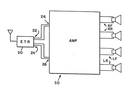
Fi~. 1 illustrates a complete automotive sound
system in block diagram form. The system "head end"
comprises an electronically tunable radio (ETR) 20, such
as the model E5VF-18B865-BA ETR available from Ford
Motor Company. The two channel outputs 22, 24 of the
ETR 20 provide signals to the right side ~26) and left
side (28) of a two-input channel to four-output channel
amplifier 30. Amplifier 30 incorporates differential
input and equalization, a hass contour control and a
power amplifier for each of the four channels. In
addition, the amplifier 30 incorporates an inverter for
boosting the nominal -~ 14 VDC automobile supply to + 28
VDC to operate the amplifier 30 circuitry. The
amplifier 30 also incorporates on/off muting for all
four channels and short circuit detection for all four
channels. The four channels in the illustrative
embodiment are right front (RF), left front (LF), right
rear (RP~) and left rear (LR). Different equalization
and bass contouring are provided depending upon whether
a channel is a front channel or rear channel. Different
signals are, of course, supplied to right and left,
thereby providing four output channels from the right
and left input channels. In the discussion that
~ollows, only a single output channel will be described,
although it is to be understood that four such channels
are provided. Where there are differences between front
and rear channels, these differences will be no-ted. The
inverter, on/off muting and short circuit detector
circuits, which are common to all four channels, will
also be discussed.
1~ 3~ 3
Turning now to Fig. 2a, a channel 32,
illustratively RF, has signal input terminals 34, 36,
which are coupled across the R output of the ETR 20. It
is to be understood that the output signal from the ETR
20, whether R or L, may already have some equalization
incorporated into it by signal processing within the
ETR. Therefore, the signal processing which is achieved
in the representative channel 32 is designed to use
advantageously that prior equalization achieved within
the ETR. However, even if no signal processing to
perform equalization has been provided by the ETR,
suitable equalization can be achieved within the channel
32.
In any event, signal is coupled from terminals
34, 36 through series 33 K resistors to the
non-inverting (~) and inverting (-) input terminals of a
differential amplifier 38 in the difEerential input and
equalization circuit 40 of channel 32. If the channel
were a rear channel, the series resistors would be 22 K
resistors. The ~ input terminal of differential
amplifier 38 is coupled to ground through a parallel RC
combination including a 100 pF capacitor and 10 K
resistor. A similar parallel RC circuit including a 100
pF capacitor and a 10 EC resistor is coupled between the
- input terminal of differential amplifier 38 and the
output terminal of differential amplifier 38. A
parallel RC circuit including a 47 pF capacitor and a
5.1 K resistor is coupled between the output terminal of
differential amplifier 38 and the + input terminal of a
differential amplifier 54. The - input terminal of
3~
di~erential amplifier 54 is coupled through a parallel
RC circuit includinq a 47 pF capacitor and a 5.1 K
resistor to the output terminal of differential
amplifier 54.
For convenience in adapting channel 32 to
different vehicle interior characteristics which can
dramatically affect the vehicle's interior sound
characteristics~ three different equalization gyrators
are also provided on the board on which the differential
input and equalization circuit 40 is mounted. The first
of these gyrators, a gyrator 56, includes a series
string of a capacitor 58, a capacitor 60 and a resistor
62, the other terminal of which is coupled to circuit
ground. The junction of capacitor 58 and capacitor 60
is coupled through a series resistor 64 to the - input
terminal of a differential amplifier 68. The junction
of capacitor 60 and resistor 62 is coupled to the ~
input terminal of differential amplifier 68. The output
terminal of differential amplifier 68 is coupled
directly to its - input terminal.
The second gyrator 70 includes a series string
of a capacitor 72, a capacitor 74 and a resistor 76, the
other terminal of which is coupled to ground. The
junction of capacitors 72, 74 is coupled through a
series resistor 78 to the - input terminal of a
differential amplifier 80. The junction of capacitor 74
and resistor 76 is coupled to the ~ input terminal of
differen-tial amplifier 80. The output terminal of
differential am~lifier 80 is coupled to its - input
terminal.
~3"~3~
- 15 -
A third gyrator 82 includes a series string of
a capacitor 84, a capacitor 86 and a resistor 88, the
other terminal of which is coupled to ground. The
junction of capacitors 84, 86 is coupled through a
series resistor 90 to the - input terminal o~ a
differential amplifier 92 in gyrator 82. The junction
of capacitor 86 and resistor 88 is coupled to the +
input terminal of this di~ferential amplifier 92. The
output terminal of differential amplifier 92 is coupled
to its -input terminal. The following table provides
values for capacitors 58, 60, 72, 74, 84, 86 and
resistors 62, 64, 76, 78, 88, and 90, for channel 32,
whether channel 32 is a front channel or a rear channel.
TABLE I
GYRATOR R AND C VALUES FOR FRONT AND REAR CHANNELS
Component Front Rear
64 6190 ohms 4990 ohms
62 49.9 K 200 K
58 .0033 uF .01 uF
.0047 uF .001 uF
78 1620 ohms 7870 ohms
76 115 K 294 K
72 .027 uF .01 uF
74 .0047 uF .001 uF
6340 ohms 1130 ohms
88 88.7 K 30I K
` - ~29~3~
6~005-~55
'I'ABL~ I (Con't)
Component Front Rear
84 .033 uF .22 uF
8~ .015 uF .00~7 uF
If attenuation is sought in connection with the
e~ualization function of any one or more of gyrators 56, 70, 82, a
jumper is coupled between the ~ input terminal of differential
amplifier 54 and the input terminal ~4, 96, 98 of that particular
gyrator 56, 70 or 82, respectively. If amplification is sought in
lo connection with the equalization function of any one or more of
gyrators 56, 70 or 82, a jumper is connected between the - input
terminal o~ differential amplifier 54 and the input terminal 94,
96 or 98 of that particular gyrator 56, 70 or 82, respectlvely.
As used in the specification and claims, the term "equalization
pole" is used to encompass both of these situations (attenuation
and amplification).
The output terminal of differential amplifier 54 is
coupled through a .1 uF capacitor 100 and a resistor 102 to the
output terminal of a feedback amplifier 104. The common terminal
of capacitor 100 and resistor 102 is coupled to one terminal of a
.1 uF capacitor 106. The remaining terminal of capacitor 106 is
coupled through a resistor 108 to the output terminal of amplifier
104. The values of resistors 102, 108 depend upon whether the
channel 32 is a F channel or a R channel. For the illustrated F
channel, the values of resistors 102, 108 are 5.1 K. If the
channel 32 were a R channel, the values of resistors 102, 108
would suitably be 10 K.
The common terminal of capacitor 106 and resistor 102 is
coupled to the ~ input terminal of a
16
:
3~3~a
~- 17 -
differential amplifier 110 which forms the input stage
` of the bass contour control circuit 112. The output
terminal of differential amplifier 110 is coupled to its
-input terminal, and through a 10 K series resistor to
the - input terminals of two differential amplifiers
114, 116. Amplifiers 114, 116 are transconductance
amplifiers. The output terminal o differential
amplifier 114 is coupled to its - input terminal, and to
ground through a 680 pF capacitor 118. The ~ input
terminal of differential ~mplifier 114 is coupled to
ground through a 8.2 ohm resistor, and through a 15 K
resistor to the wiper of a distortion trimming 10 K
potentiometer, the terminals of which are coupled to +
15 VDC supplies.
The + input terminal of differential amplifier
116 is coupled to ground. The output terminal of
differential amplifier 116 is coupled through a series 2
K resistor to the - input terminal of differential
amplifier 110. The output terminal of differential
amplifier 116 is also coupled to ground through series
peaking resistor 128. If the channel is a F channel,
the value of resistor 128 is illustratively 47 K. If
the channel 32 is a R channel, the value of resistor 128
is illustratively 39 K. The output terminal of
differential amplifier 116 is also coupled to the
! input terminal of amplifier 104.
The output terminal of differential amplifier
110 is coupled through a series string of a 22 uF
capacitor 130, a 22 uF capacitor 132 and a 910 ohm
resistor 134 to ground. The common terminal of
~ 293~3~
- 18 -
capacitor 132 and resistor 134 is coupled to the - input
terminal of a differential amplifier 136 which forms the
input stage of the power amplifier 140 o~ channel 32.
The output terminal of differential amplifier 136 is
coupled through a parallel RC circuit including a 2.4 K
resistor 142 and a 47 pF capacitor 144 to one terminal
of a 47 pF capacitor 146. The remaining terminal of
capacitor 146 is coupled through a parallel circuit
including a 47 pF capacitor 148 and an 11 K resistor 150
to the + input terminal of differential amplifier 1~6.
The + input terminal of differential amplifier
136 is also coupled to ground through a 1 K resistor
152. The common terminal of resistor 142 and capacitors
144, 146 is coupled to the anodes of two diodes 154,
156. The cathode of diode 154 is coupled to the output
terminal of the on~off muting circuit 158 (Fig. 2b).
The cathode of diode 156 is coupled to the emitter of a
transistor 160. The base of transistor 160 is coupled
to ground and its collector is coupled to the anode of a
diode 161, the cathode of which is coupled through a 220
ohm series resistor 162 to the - 28 VDC supply provided
by the inverter 164.
The anode of a diode 171 is also coupled to the
collector of transistor 1~0. The cathode of diode 171
is coupled to the cathode of a diode 172, the anode of
which is coupled to an input terminal, pin 7 of output
stage 170. The cathode of diode 154 is coupled to the
cathode of a diode 173, the anode of which is coupled to
the anode of a diode 174. The cathode of diode 174 is
coupled to an input terminal, pin 1 of output stage
~a-~3~
- 19 --
170. A .1 uF capacitor 175 is coupled across pins 1, 7
of output stage 170.
~ 28 VDC is coupled to pin 2 of output stage
170. - 28 VDC is coupled to pin 6 of output stage 170.
~ 28 VDC is also coupled through a 1 K resistor to the
base of a transistor 179. The base of transistor 179 is
coupled to the anode of a diode 176, the cathode of
which is coupled through a 27 K resistor to ground. The
cathode of diode 176 is also coupled to the cathode of a
diode 177, the anode of which is coupled to the anodes
of diodes 173, 174 and the collector of transistor 179.
The emitter of transistor 179 is coupled through an 82
ohm resistor to ~ 28 VDC.
The cathodes of diodes 171, 172 are coupled to
the collector of a transistor 178. The base of
transistor 178 is coupled to the cathode of diode 161.
The emitter of transistor 178 is coupled through a 10
ohm resistor to - 28 VDC.
Components 154, 156, 160, 161, 162 and 171-179
and their associated circuits comprise the drive and
bias offset networks for the input terminals, pins 1, 7
of output stage 170.
The output terminal, pin 4, of output stage 170
is coupled through series resistors 180, 182 of 220 ohms
and 100 ohms resistance, respectively, to pins 3 and 5
of output stage 170. The output terminal of output
stage 170 is also coupled through a series 2.7 ohm 1/2
watt resistor and a .1 uF capacitor to ground. The
common terminal of resistors 180, 182 is coupled to the
base of a transistor 184, the collector of which is
~3~3~
- 20 --
coupled through a 10 K series resistor to an input
terminal of short circuit detector circuit 186 ~Fig.
2b). The emitter of transistor 184 is coupled to pins 3
and 5 of output stage 170. The output terminal, pin 4,
of output stage 170 is coupled to the common terminal of
capacitors 146, 148 and resistor 150, to the + terminal
of the speaker connector 188 for channel 32, and to an
11 K resistor 190 of a series RC circuit which also
includes a capacitor 192. The - terminal of speaker
connector 188 is connected to ground.
If channel 32 is an F channel, the value of
capacitor 192 illustratively is .15 uF. If channel 32
were a R channel, the value of capacitor 192
illustratively would be .22 uF. The common terminal of
resistor 190 and capacitor 192 is coupled to one
terminal of a 100 K resistor 194. The other terminal of
resistor 194 is coupled through a capacitor 19~ to
ground. If channel 32 is a F channel, the value of
capacitor 196 is illustratively .033 uF. If channel 32
were a R channel, the value of capacitor 196
illustratively would be .047 uF.
The speaker drive signal from the output
terminal of output stage 170 to speaker connector 188 is
fed ~ack through the network including resistor 190,
capacitor 192, resistor 194, capacitor 196 and a series
RC circuit including a .1 uF capacitor 198 and a 100 K
resistor 200 to the ~ input terminal of an amplifier
202. The cathode of a diode 204 is coupled to the +
input terminal of amplifier 202. The anode of diode 204
is coupled to the - input terminal of amplifier 202, and
3~3~
-- 21 -
through a threshold setting resistor 206 to the ~ 15 ~DC
supply. Illustrative values for resistor 206 are 820 K
for the ~ channels and 1 M for the R channels. A 100 K
feedback resistor is coupled between the output terminal
of amplifier 202 and the - input terminal thereof. The
anode of a diode 210 is coupled to the output terminal
of amplifier 202. The cathode of diode 210 is coupled
to the cathode of a diode 212. If diode 210 is in the
RF channel, diode 212 is in the corresponding location
in the LF channel. Therefore, the anode of diode 212 is
coupled to the output terminal of an amplifier which
occupies the same position in the LF channel as does
amplifier 202 in the RF channel. Similarly, if diode
210 were in the RR channel, diode 212 would occupy the
same position in the LR channel.
The cathodes of diodes 210, 212 are coupled
through a 3.3 K series resistor to the + input te~minal
of an amplifier 216. The output terminal of amplifier
216 is coupled through a parallel RC feedback circuit
including a capacitor 218 and a resistor 220 to the -
input terminal of amplifier 216. If the illustrated
channel 32 is a F channel, the capacitance of capacitor
218 is illustratively .47 uF and the resistance of
resistor 220 is illustratively ~7 K. If the illustrated
channel 32 were a R channel, the capacitance of
capacitor 218 illustratively would be 1.0 uF, and the
resistance of resistor 220 illustratively would be 12
K. A signal is coupled from the output terminal of
amplifier 216 through a 2.4 K resistor and a 22 uF
capacitor to ground. The common terminal of this
~3~3~
- 22 -
resistor and this capacitor is coupled through a series
.4 K resistor to the - input terminal of an amplifier
226 and to the drain terminal of an FET 228. The gate
terminal o FET 228 i5 coupled to the output terminal of
amplifier 226. The + input terminal of amplifier 226 is
coupled to ground. The source terminal of FET 228 is
coupled through a series 13 K resistor to the gain
control terminal, pin 16, of differential amplifier 116
in the bass contour control circuit 112. A
corresponding 13 K resistor 232 couples the source of
FET 228 to the corresponding pin of an amplifier
corresponding to amplifier 116 in the other F or R
channel. For e~ample, if the illustrated channel 32 is
a RF channel, resistor 232 is coupled to the
corresponding pin of an amplifier corresponding to
amplifier 116 in the LF channel. Similarly, if channel
32 were a RR channel, resistor 232 would couple the
source of FET 228 to pin 16 of an amplifier
corresponding to amplifier 116 in the LR channel. It
should be noted that amplifiers 216 and 226 and FET 228
and their associated passive components are not
duplicated in the other F or R channel of the pair RF
and LF or RR and LR. In other words RF and LF share a
single circuit including amplifiers 216 and 226 and FET
228. Similarly, RR and LR share a single circuit
including amplifiers 216 and 226 and FET 228. Referring
to Fig. 2b, it is also to be understood that a single
on/off muting circuit 158, a single inverter circuit 164
and a single short circuit detector circuit 186 are
provided for all four channels RF, LF, RR, LR.
3~3~3~
- 23 -
Turning now to the inverter circuit 164, a
remote on/off switch ~not shown) supplies nominal ~ 14
VDC at a terminal 242. A 10 K resistor and a Zener
diode 245 are coupled in series between terminal 242 and
ground. The caihode of Zener diode 245 is coupled to
the base of transistor 247, the emitter of which is
coupled through a 47 ohm resistor to a terminal, pin 12,
of an inver-ter integrated circuit 246. Circuit 246
generates switching waveforms for the inverter circuit
164. The pin numbers illustrated in Fig. 2b are for a
Texas Instruments type TL 594 inverter integrated
circuit 246. ~owever, it is to be understood that any
other suitable inverter switching waveform generator
could be used.
Pins 8, 11 of circuit 246 are coupled directly
to pin 12. A 22 uF capacitor is coupled between pins 8,
11, 12 and pin 7 of circuit 246, the inverter common
terminal. Pins 1, 3 of circuit 246 are joined and are
coupled through a series 2.4 K resistor to pin 7 of
circuit 246. Pin 5 is coupled through a .0047 uF
capacitor to pin 7. Pin 6 is coupled through a 2.4 K
resistor to pin 7. Pins 2 and 15 of circuit 246 are
coupled to both the collector and base of a transistor
254. The emitter of transistor 254 is coupled to pin 7
of circuit 246. The collector and emitter of transistor
254 are coupled together by a series string of a 6.8 K
resistor 255, a 6.8 K resistor 257, a 500 ohm
potentiometer 259 and a 470 ohm resistor 261. The
common terminal of resistors 255, 257 is coupled to
terminals 13, 14 of circuit 246. The emitter of a
3~3~L
- 2~ ~
transistor 256 is coupled to pins 13, 14 of circuit
246. Pins 13, 14 are also coupled through a series 22
uF capacitor to pin 4 of circuit 246. Pin 16 of circuit
246 is coupled to the common terminal of resistor 257
and potentiometer 259. The collector of transistor 256
is coupled to pin 4 of circuit 246, and through a 10 K
resistor to pin 7 of circuit 2~6. A resistive voltage
divider comprising two 1 K rasistors is coupled between
terminal 242 and pin 7 of circuit 246. The junction of
these two 1 K resistors is coupled to the base of
transistor 256.
~ The output terminals, pins 9, 10 of circuit 246
are coupled, respectively, to the bases of transistors
260, 262. The bases of transistor 260, 262 are coupled
through series 1 K resistors to pin 7 of circuit 246.
The collectors of transistors 260, 262 are coupled to
pin 7. The emitters of transistors 260, 262 are coupled
to the cathodes of diodes 268, 270, respectively, the
anodes of which are coupled to the bases of transistors
260, 262, respectively.
An inverter transformer 272 includes a primary
winding 274 having end terminals 276, 278 and a center
tap 280. End terminal 276 is coupled to the cathode of
a Zener diode 282, the anode of which is coupled to the
anode of a diode 284. A 47 pF capacitor is coupled
between the cathodes of diodes 282, 284. The cathode of
diode 284 is coupled to pin 9 of circuit 246. End
terminal 278 is coupled to the cathode of a Zener diode
286, the anode of which is coupled to the anode of a
diode 288. A 47 pF capacitor is coupled between the
~2~3~31
- 25 ~-
cathodes of diodes 286, 288. The cathode of diode 288
is coupled to pin 10 of circuit 246. The emitter of
transistor 260 is coupled to the gate electrodes of
three FETs 290 whose source and drain terminals are
connected in parallel. For purposes of simplifying the
circuit diagram, only one of these FETs 290 is
illustrated. The sources of all of these FETs 290 are
coupled to pin 7 of circuit 246. The drains of all of
FETs 290 are coupled to end terminal 276. The emitter
of transistor 262 is coupled to the gate electrodes of
three FETs 292 whose source and drain terminals are
connected in parallel. Again, for purposes of
simplifying the circuit diagram, only one of these FETs
292 is illustrated. The sources of FETs 2~2 are coupled
to pin 7 of circuit 246. The drains of FETs 292 are
coupled to end terminal 278. Center tap 280 of primary
274 is coupled through two parallel 470 uF, 25 ~
capacitors to chassis ground. In order to simplify the
circuit diagram, only one of these 470 uF capacitors îs
illustrated. Pin 7 is coupled to the chassis ground.
The center tap 280 of primary winding 274 is also
coupled through a 3uH choke and 470 uF capacitox to
ground. The common terminal of the 3 uH choke and 470
uF capacitor is coupled through a 20 ampere fuse 296 and
a 10000 uF capacitor to ground. The common terminal of
the fuse 296 and the 10000 uF capacitor is coupled
through a 1.2 mH choke to nominal ~ 1~ VDC.
The secondary winding 298 of inverter
transformer 272 includes end terminals 300, 302 and a
center tap 304. The center tap 304 is coupled to
3~3~
ground. The cathode of a diode 306 and the anode of a
diode 308 are coupled to end terminal 300. The cathode
of a diode 310 and the anode of a diode 312 are coupled
to end terminal 302. The anodes of diodes 306, 310 are
joined, as are the cathodes of diodes 308, 312. Diodes
306, 308, 310, 312 thus form a full-wave bridge
rectifier for the voltage variations appearing across
secondary winding 298. The anodes of diodes 306, 310
are coupled through a 470 uF, 35 V capacitor 314 to
ground, and through a 3 uH choke 316 to an input
terminal of a 15 VDC regulator 318. The cathodes of
diodes 308, 312 are coupled through a 470 uF, 35 V
capacitor 320 to ground, and through a 3 uH choke 322 to
an input terminal of a 15 VDC regulator 32~. The common
terminals of regulators 318, 324 are coupled to ground.
The output terminals of regulators 318, 324 are coupled
through respective 10 ohm resistors 325 and 327 and 22
uF capacitors 326, 328 in series to ground. - 15 VDC is
available across capacitor 326. ~ 15 VDC is available
across capacitor 327.
Two 220 uF capacitors in parallel are coupled
between the input terminal of regulator 318 and ground.
Only one of these capacitors, capacitor 330, is
illustrated in the circuit diagram for purposes of
simplification. - 28 VDC is available at the ungrounded
terminal of capacitor 330. Two parallel 220 uF
capacitors are coupled between the input terminal of
regulator 324 and ground. Again, onl~ one of these
capacitors, capacitor 332, is illustrated for purposes
of simplification. ~ 28 VDC is available at the
3~
ungrounded terminal of capaci~or 332. The drive signals
a~ailable at pins 9, 10 of circuit 246 are amplified by
transistors 260, 262, respectively, and drive the 3
parallel FETs represented by each o~ FETs 290, 292. The
switching of end terminals 276, 278 to ground which
results from these driving signals causes voltage
variations ~o appear across sacondary ~inding 298.
These voltage variations are rectified in the full-wave
bridge 306, 308, 310, 312 and filtered by the respective
filters 314, 316 and 320, 322 to provide the operating
voltages for the illustrated circuits.
The on~off muting circuit 158 of Fig. 2
includes a transistor 336, the base of which is coupled
through a 100 K series resistor to end terminal 302 of
secondary 298. The base of transistor 336 is also
coupled through a 10 K resistor to ground. The emitter
of transistor 336 is coupled to ground. The collector
of transistor 336 is coupled to the base of a transistor
342, through a 47 K series resistor to + 28 VDC, and
through a .01 uF capacitor to ground~ The emitter of
transistor 342 is coupled to ground. Its collector is
coupled to the base of a transistor 348, through a 1.5 M
resistor to + 28 VDC and through a 22 uF capacitor to
ground. The collector of transistor 348 is coupled
through a 10 K resistor to + 28 VDC. Its emitter is
coupled to the base of a transistor 356. The collector
of transistor 356 is coupled to the base of an on/off
muting circuit output transistor 360, and through a 10 K
series resistor to ~ 28 VDC. The emitters of both of
transistors 356, 360 are coupled to ground. The
1~3~
- 28 -
collector of transistor 360 forms the muting ci.rcuit 15
output terminal 362. The muting signal is derived rom
end terminal 302 of secondary winding 298 in the
inverter circuit 240. This signal drives, through the
various stages 336, 3~2, 348, 356, 360 the muting output
terminal 362. The power amplifiers 140 of all four (~F,
RR, LF, LR) channels 32 are coupled to muting circuit
output terminal 3~2.
Similarly, the power amplifiers 140 of all four
channels are coupled to the short circuit detector
circuit 186 input terminal 363. Input terminal 363 of
short circuit detector circuit 186 is coupled to the
base of a transistor 364. The emitter of transistor 364
is coupled through a parallel RC circuit including a 1 K
resistor 366 and a .1 uF capacitor 368 to its base. The
emitter of transistor 364 is also coupled to + 28 VDC
supply. The cathode of a Zener diode 370 is coupled to
the emitter of transistor 364. The anode of Zener diode
370 is coupled to the collector of transistor 364. The
20. collector of transistor 364 is coupled through a series
10 K resistor to pins 1, 3 of the inverter drive signal
generator integrated circuit 246. If a short circuit
appears across any of the power amplifier 140 speaker
connector 188 terminals, transistor 184 in the channel's
power amplifier 140 is turned off, resulting in turning
of transistor 364 off. This results in a low voltage
condition at pins 1, 3 of the inverter drive signal
generator integrated circuit 246. This removes drive
signal from pins 9, 10 of circuit 246, which results in
fairly rapid decay of the + 28 VDC, + 15 VDC, - 15 VDC
and - 28 VDC supplies.
3~
- 29 -
The following is a table of the active
components of the circuit of Fig, 2 with illustrative
types and sources.
TABLE II
Active Component Type and Source
38 1/2 LF353 National Semiconductor
54 1/4 LF347 National Semiconductor
6B 1/4 LF347 National Semiconductor
lf4 LF347 National Semiconductor
92 1~4 LF347 National Semiconductor
104 1/4 LF347 National Semiconductor
110 1/4 LF347 National Semiconductor
114 1/2 LM13600 National Semiconductor
116 1~2 LM13600 National Semiconductor
136 1/2 5532 Signetics
154 lN4148
156 lN4148
160 2N3906 Motorola
161 lN414B
170 1~2 STK2240 Sanyo
171 lN4148
172 lN4148
173 lN4148
174 lN4148
176 lN4148
177 IN4148
178 MPS8099 Motorola
179 MPS8599 Motorola
~3~3~
- 30 -
TABLE II ~Con't)
Active Component T~pe _nd Source
184 MPS8099 Motorola
202 1/4 LM3900 National Semiconductor
204 lN4148
210 lN4148
212 lN4148
216 1/4 LM3900 National Semiconductor
226 1/4 LM3900 National Semiconductor
228 2N4360 Motorola
245 lN4112
246 TL-594 Texas Instruments
247
254 TIP31C
256 2N4403 Motorola
260 2N4403 Motorola
262 2N4403 Motorola
268 lN4148
270 lN4148
282 lN5259
284 lN4148
286 lN5259
288 lN4148
290 3 BUZ71A Seimens/International
Rectifier
292 3 BUZ71A Seimens/International
RectiEier
306 1/2 TG284A Varo
308 1/2 TG284 Varo
3~
- 31 -
TABLE XI (Con't)
Active Component Type and Source
310 1~2 TG284A Varo
312 1/2 TG284 Varo
318 7915 Motorola
324 7815 Motorola
336 2N3904 Motorola
342 2N3904 Motorola
348 2N3904 Motorola
356 2~3904 Motorola
360 2N3904 Motorola
364 2N4403 Motorola
370 lN5259