Language selection

Search

Patent 1293993 Summary

Third-party information liability

Some of the information on this Web page has been provided by external sources. The Government of Canada is not responsible for the accuracy, reliability or currency of the information supplied by external sources. Users wishing to rely upon this information should consult directly with the source of the information. Content provided by external sources is not subject to official languages, privacy and accessibility requirements.

Claims and Abstract availability

Any discrepancies in the text and image of the Claims and Abstract are due to differing posting times. Text of the Claims and Abstract are posted:

  • At the time the application is open to public inspection;
  • At the time of issue of the patent (grant).
(12) Patent: (11) CA 1293993
(21) Application Number: 574576
(54) English Title: D.C. POWER MONITOR
(54) French Title: CONTROLEUR DE TENSIONS CONTINUES
Status: Deemed expired
Bibliographic Data
(52) Canadian Patent Classification (CPC):
  • 324/58
(51) International Patent Classification (IPC):
  • G01R 19/165 (2006.01)
  • G05F 1/571 (2006.01)
(72) Inventors :
  • WHITE, RANDALL A. (United States of America)
(73) Owners :
  • WHITE, RANDALL A. (Not Available)
  • DIGITAL EQUIPMENT CORPORATION (United States of America)
(71) Applicants :
(74) Agent: SMART & BIGGAR
(74) Associate agent:
(45) Issued: 1992-01-07
(22) Filed Date: 1988-08-12
Availability of licence: N/A
(25) Language of filing: English

Patent Cooperation Treaty (PCT): No

(30) Application Priority Data:
Application No. Country/Territory Date
085,095 United States of America 1987-08-13

Abstracts

English Abstract


ABSTRACT OF THE DISCLOSURE
A DC power monitor includes a reference
voltage and voltage dividers for obtaining voltages
which are respectively above and below the
reference level when the voltages being monitored
are at their nominal value. Comparators compare
the divided voltages with the reference and the
comparator outputs are Anded and coupled through a
flip flop to a bicolor LED which is one color when
the voltages are in tolerance and another color
when out of tolerance.


Claims

Note: Claims are shown in the official language in which they were submitted.


61293-185

THE EMBODIMENTS OF THE INVENTION IN WHICH AN EXCLUSIVE
PROPERTY OR PRIVILEGE IS CLAIMED ARE DEFINED AS FOLLOWS:

1. A DC power monitor for monitoring at least first and
second voltages comprising: means for establishing a reference
voltage level from a third voltage source; first means for
dividing said first voltage to obtain a first divided voltage
higher than said reference voltage when said first voltage is at
its nominal level; a first comparator for comparing said first
divided voltage and said reference voltage to provide a first
output having a first-level when said first divided voltage is
above said reference voltage and a second level when below; second
means for dividing said second voltage to obtain a second divided
voltage higher than said reference when said second voltage is at
its nominal value; a second comparator for comparing said second
divided voltage with said reference having an output at said first
level when said second divided voltage is above said reference
voltage and a second level when below; third means for dividing
said first voltage to obtain a third divided voltage lower than
said reference voltage when said first voltage is at its nominal
value; a third comparator for comparing said third divided voltage
with said reference voltage and providing an output at said first
level when said third divided voltage is lower than said reference
voltage and of said second level when above; fourth means for
dividing said second voltage to obtain a fourth divided voltage
lower than said reference voltage; a fourth comparator for
comparing said fourth divided voltage with said reference voltage
and providing an output at said first level when said third


61293-185
divided voltage is lower than said reference voltage and of said
second level when above; said first and second voltages being
respectively positive and negative voltages, wherein said third
source voltage is also a positive voltage and wherein said first
voltage of said first and third voltage dividing means is coupled
to one end of its respective voltage dividing means with the other
end thereof coupled to ground and said second, negative voltage of
said second and fourth voltage dividing means is coupled to one
end of its respective voltage dividing means with the other end
thereof coupled to said third source voltage, whereby in each case
positive voltages can be provided as inputs to said comparators
for comparison with said positive reference voltage; means for
Anding the outputs of said first, second, third and fourth
comparators; an LED with first and second cathodes providing two
colors; and means having as an input the output of said means
Anding said comparator signals, said means providing first and
second outputs to said first and second cathodes for respectively
energizing a first and second color thereof, said means providing
a signal which energizes one color of said LED when a signal is
present from said Anding means and energizing the other color when
said signal is not present from said Anding means.


2. Apparatus according to claim 1 wherein each of said
dividing means comprises a resistor voltage divider.


3. Apparatus according to claim 2 wherein the said
reference voltage is provided as an input to the inverting inputs


61293-185
of said first and second comparators with the outputs of said
first and second voltage dividers provided to the non-inverting
inputs thereof and wherein said reference voltage is provided to
the non-inverting inputs of said third and fourth comparators and
the outputs of said third and fourth voltage dividers are provided
as inputs to the inverting inputs thereof.

4. Apparatus according to claim 3 wherein said means for
Anding comprise a first And gate for Anding the outputs of said
first and third comparators; a second And gate for Anding the
outputs of said second and fourth comparators; and a third And
gate for Anding the outputs of said first and second And gates.

5. Apparatus according to claim 4 wherein said means for
energizing comprise: a D type flip flop having its preset input
coupled to the output of said third And gate and having its D
input coupled to ground to provide a logic 0 signal; means
providing a clock signal; and means coupling said clock signal to
the clock input of said flip flop whereby, when a signal is
present from said third And gate indicating that a voltage is out
of range, said flip flop will be preset providing a logic "1"
signal on its "1" output and a logic "0" signal on its "0" output
to energize a first cathode of said LED and whereby, if said
preset input is not present, said clock will clock to said logic
"0" signal at its D input to its "1" output to thereby cause a
logical "1" level to be present on the "0" output of said flip
flop to energize the other cathode of said LED.

11


61293-185
6. Apparatus according to claim 5 wherein said LED has red
and green cathodes and wherein said output indicating a voltage
out of tolerance energizes said red cathode and said output
indicative of normal operation energizes said green cathode and
wherein an absence of any light is indicative of a failure of said
third power supply.
7. A method for monitoring at least first and second DC
voltages being positive and negative voltages, respectively,
comprising: establishing a reference voltage level from a third
voltage source, said third voltage source being a positive
voltage; coupling said first voltage to one end of a first and
second means for dividing and coupling the other end to ground;
dividing the first voltage in the first dividing means to obtain a
first divided voltage higher than said reference voltage;
comparing said first divided voltage with said reference voltage
to provide a first output; dividing said first voltage in the
second dividing means to obtain a second divided voltage lower
than said reference voltage; comparing said second divided voltage
with said reference voltage to provide a second output; coupling
said second voltage to one end of a third and fourth means for
dividing and coupling the other end to the third voltage, whereby
in each case positive voltages can be provided as inputs for
comparing with the reference voltage; dividing said second voltage
in the third dividing means to obtain a third divided voltage
lower than said reference voltage; comparing said third divided
voltage with said reference voltage to provide a third output;

12

61293-185
dividing said second voltage in the fourth dividing means to
obtain a fourth divided voltage higher than said reference
voltage; comparing said fourth divided voltage with said reference
voltage to provide a fourth output; Anding said first, second,
third and fourth outputs to obtain a fifth output; and energizing
one color cathode of a two color LED if said fifth output is
present and the other cathode if said fifth output is not present.

8. A method according to claim 7 wherein the step of
coupling to said first, second, third and fourth dividing means is
carried out by coupling to a first, second, third and fourth
resistor divider respectively.


9. A method according to claim 8 wherein the step of
energizing is carried out with a D type flip flop.

13

Description

Note: Descriptions are shown in the official language in which they were submitted.


93

6~293-185
RELATED APPLICATIO S
This application is related to the following
applications. These applications contain, at least ln part,
common disclosure regarding an embodiment of a peripheral repeater
box. Each, however, contains claims to a different invention.
Canadian Patent Applicakion Serial No. 574,394 filed on
August 11, 1988, Canadian Pa~ent Application Serial No. 574,585
filed on August 12, 1988 and Canadian Patent Application Serial
No. 574,290 filed on August 10, 1988.
BACKG~OUND OF THE INVE~TIO~
This invention xelates to electronic systems in general
and more particularly, to a D.C. power monitor for use in a system
which includes a plurality of power supplies.
Various electronic systems, such as the peripheral
repeater box described in the above identified applications
requixe a number of


.~ 1

~3
2 --


different power supplies. Thus, an indicatlon of
the proper operation of these supplies is quite
desirable.

~UMNARY OF ~HE INVENTION

In accordance with the present invention, a
DC power monitor is provided to monitor a plurality
of power supplies and indicates power status with a
bicolor LED. This monitor provides a rough
indication of positive and negative 12 volt power
supplies. If either supply is out of spec 10 to 15
percent then the LED will indicate a failure by
changing its color. The DC power monitor is itself
powered by a 5 volt supply. If the LED is out,
this indicates failure o~ the 5 volt supply.
Although disclosed in conjunction with + 12 volts
supplies and a 5 volt supply, the invention is, of
course, applicable to other voltages.

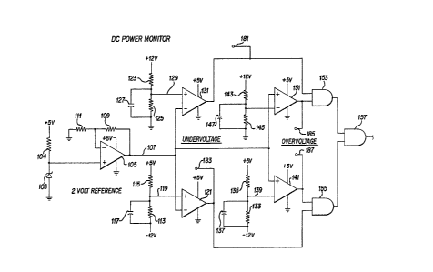
3RI~F DE8CRIPTION OF ~ DRAWTNG

The single Figure is a schematic diagram of
the DC power monitor of the present invention.

DETAILE~ DE8CRIPTION

The single figure illustrates an embodiment
of the DC power monitor of the present invention.
The circuitry to monitor the plus and minus 12v


supplies operates from the +5v. supply. A single
red/green bicolor LED is connected to.the output of
the power monitor circuit. The output indicators
are as follows:

LED Indication Dsscription

Green All voltages present and within
range
Red Either plus, minus or both 12
volt supplies are approximately
15% out of spec or dropped out
completely
None +5v supply, all supply voltages
dropped out or no AC

The DC power monitor is a set of four
comparators to check undervoltage and overvoltage
out of range approximately 15% at nominal for the
plus and minus 12 volt supplies. The circuit runs
from plus five volts and uses a plus two volt
precision reference applied to the appropriate
reference input of each comparator. The output is
connected to bicolor LED 64. Precision resistor
dividers connected to the other input of each
comparator, scale the test voltage down to the same
range as the reference input.

The +5 volt supply is coupled across a
series circuit of a resistor 101 and Zener diode
103. Zener diode 103 is a 1.25 volt Zener diode.

~2~3~9~
-- 4


Tha junction between resistor 101 and zener diode
103 is coupled to the non-inverting input of an
amp~ifler 105. Amplifier 105 has its output on
line 107 coupled through a resistor 109 to its
inverting input. Also coupling the inverting input
to ground is a resistor 111. In the preferred
embodiment, resistor 109 has a resistance of 15k
and resistor 111 a resistance of 24.3K. This gives
a gain for amplifier 105 which results in a 2 volt
output on line 107.

The -12 volt supply is coupled to a
resistor 113 which is in series with a resistor 115
which has its other end coupled to the +5 volt
supply. A capacitor 117 is coupled in parallel
across resistor 113. Resistor 113, in the
preferred embodiment, has a value of 15.8R and
resistor 115 a value of 3.01K. If the -12 volt
supply is exactly at -12 volts and the +5 volt
supply at -~5 volts, the resulting voltage at the
junction between the two resistors, i.e., on line
119 will be approximately 2.8 volts. This 2.8
volts is compared with the 2 volts on line 107 in
comparator 121.

The +12 volts supply is coupled to a
resistor 123 in series with a resistor 125 which is
connected to ground. Again, a capacitor 127 is
coupled across resistor 125. The value of resistor
123 in the preferred embodiment is 8.25k and the
value o~ resistor 125, 2.2k. Capacitors 117 and

3~3


127 are each prefera~ly 0.01 microfarad~ If the
+12 volt supply is exactly 12 volts, with this
divider, the voltage at the junction, i.e., on line
129 will also be above 2 volts. This voltage is
compared in comparator 131 with the output of line
107.

In the case of comparator 121, the voltage
to the non-inverting input from the voltage
divider, if the full -12 volts is present, will be
above the 2 volts on line 107. This will result in
a high or logic ~16' output from the respective
comparators If the -12 voltage in question
increases, however, above a predetermined amount,
e.g. 15%, at some point the voltage on line ll9 as
the case may be, will fall below 2 volts and the
output of comparator 121 will change from a logic
nl~ to a logic ~0". Thus, comparator 121 detects
an overvoltage condition for the -12 volt supply.

Similarly, if the +12 volt supply drops by,
e.g. 15% the voltage on line 129 will fall ~elow 2
volts and the output of comparator 131 will change
from nl~r to r~on indicating an undervoltage
condition for the +12 volt supply.

To detect undervoltage on the -12 v supply,
an additional voltage divider comprising resistors
133 and 135 is provided. Resistor 133 has its open
end connected to the -12 volts supply and resistor
135, its open end to the +5 volt supply. Once

~g3~

-- 6 --


again, a capacito~ 137 is provi~ed. For the +12
supply overvoltage detection, ~12 volts is
connected across a voltage divider comprising
resistors 143 and 145 with the other side of
reslstor 145 connected to ground. Again a
capacitor 147 is provided across resistor 145.
Preferably capacitors 137 and 147 have a value of
O.Oluf. Resistor 133 has a value of 12.lK,
resistor 135 a valuè of 3.01K, resistor 143 a value
of 11.8K and resistor 145 a value of 2k. The
ratios in these resistor dividers are chosen such
that if the + and - 12 volt supplies are at their
normal levels, the voltages on lines 139 and 149
respectively will be below the 2 volt reference on
line 107. As a result, the output of the
respective comparators 141 and 151, since the
reference in this case is provided to the non-
inverting input will be positive or a logic ~1~ so
long as the voltaye level does not increase above a
predetermined amount. I~ one of the 12 volt
supplies goes above a preestablished level, then
the voltage on the inverting input of its
comparator will exceed the voltage on the non-
inverting input and the state of the comparator
will change from a logic ~1~ to a logic ~0~.

Note that for the minus 12 volt comparators
the voltage is biased up with the plus five volt
supply, this is done to keep negative voltages from
being present on the inputs of the comparator.

;3~:3~


The outputs of comparators 131 and 151 are
combined in an And gate 153. 5imilarly, the
outputs of comparators 121 and 141 are coupled to
an And gate 155. The respective outputs of these
And gates 153 and 155 are inputs to an And gate
157. And gate 157 is coupled to the preset input
of a D-type flip-flop 159. The input of this
flip-flop is coupled to ground by a line 161. Its
clear input is coupled to a ~'power up~ signal on
line 163 so that the flip-flop is cleared on power
up. Its clocking input is coupled to the output of
an And gate 165 which has as one input a clock
signal with a frequency of about 30 KHz and has as
its other input, the output of gate 157.

The logic ~1~ output of flip-flop 159 is
provided as an input to an Nand gate 167 and the
~0~ output to an Nand gate 169. 'rhe second inputs
of these Nand gates are a 3 volt signal. The
outputs of Nand gates 167 and 169 are coupled to
pull-up resistors 171 and 173 which are connected
to +5 volts. They are also coupled to the red and
green cathodes of a bi-color LED 175.

If the voltage levsls are as they should
be, there will be no output from gate 157. In that
case, the flip-flop 159 will remain in its reset
state and an output will be provided from its ~0
output into gate 169 which will provide a~ 0" or
ground level to the green cathode turning on the
the green cathode to indicate proper operation.


Should an undervoltage or overvoltage occur, the
output of gate 157 will set flip-flop 159 through
its connection to the preset input. As a result,
an output will be provided on line 177 to the red
cathode indicating that there is a problem in th~
power supply. The outputs of the four comparators
are normally high and any fault detected will ca~lse
that output to go to low setting flip flop 159.
The power problem can than be diagnosed by checking
the test points 181, 183, 185 and 187 to find out
which comparator is providing a signal indicating a
voltage is not within tolerance. Upon correction
of the defect, the preset signal is removed and the
NO~ at the D input, which is connected to ground,
is transferred to the ~1~ output. The ~on output
becomes high and the green cathode of L$D 12S is
lit.

Thus, as long as a fault condition exists
the clock will be blocked and flip flop 159 will
remain set. However, as soon as the fault
condition goes away the clock will be enabled
loading a zero in and thereby clearing flip flop
157. This has been done so that a transient
condition will not latch up the indicator but
rather that the indicator will indicate a hard
fault condition.

Representative Drawing
A single figure which represents the drawing illustrating the invention.
Administrative Status

For a clearer understanding of the status of the application/patent presented on this page, the site Disclaimer , as well as the definitions for Patent , Administrative Status , Maintenance Fee  and Payment History  should be consulted.

Administrative Status

Title Date
Forecasted Issue Date 1992-01-07
(22) Filed 1988-08-12
(45) Issued 1992-01-07
Deemed Expired 1995-07-08

Abandonment History

There is no abandonment history.

Payment History

Fee Type Anniversary Year Due Date Amount Paid Paid Date
Application Fee $0.00 1988-08-12
Registration of a document - section 124 $0.00 1989-03-13
Maintenance Fee - Patent - Old Act 2 1994-01-07 $100.00 1993-12-13
Owners on Record

Note: Records showing the ownership history in alphabetical order.

Current Owners on Record
WHITE, RANDALL A.
DIGITAL EQUIPMENT CORPORATION
Past Owners on Record
None
Past Owners that do not appear in the "Owners on Record" listing will appear in other documentation within the application.
Documents

To view selected files, please enter reCAPTCHA code :


To view images, click a link in the Document Description column. To download the documents, select one or more checkboxes in the first column and then click the "Download Selected in PDF format (Zip Archive)" or the "Download Selected as Single PDF" button.

List of published and non-published patent-specific documents on the CPD .

If you have any difficulty accessing content, you can call the Client Service Centre at 1-866-997-1936 or send them an e-mail at CIPO Client Service Centre.


Document
Description 
Date
(yyyy-mm-dd) 
Number of pages   Size of Image (KB) 
Drawings 1993-10-26 2 36
Claims 1993-10-26 5 192
Abstract 1993-10-26 1 26
Cover Page 1993-10-26 1 12
Description 1993-10-26 8 249
Representative Drawing 2002-04-09 1 11
Fees 1993-12-13 1 26