Note: Descriptions are shown in the official language in which they were submitted.
lS
DIELECTRICALLY LOADED WAVEGUID~ SWITCH
BACXG~OUND OF THE INVENTION
Field of the Invention:
The present invention relates to microwave circuits.
More specifically, the present invention relates to
switches used to connect signals from two or more
microwave channels.
While the present invention is described herein with
reference to a particular embodiment for an illustrative
application, it is understood that the invention is not
limited thereto. Those having ordinary skill in the art
and access to the teaching provided herein will recognize
additional modifications, applications and embodiments
~ within the scope thereof.
; Descri~tion of the Related Art:
:''
~ 20 Microwave switches selectively connect channels in
;~microwave circuits and systems. The two categories of
switches related to this invention are coaxial switches
and waveguide switches.
~Coaxial switches are known to have several
;25 limitations. The most severe being power handling
capability. The maximum average power that the coaxial
switch can handle is typically limited by overheating of
the internal switch materials due ~o RF losses. The
conventional designs typically result in poor thermal
conductivity from the transmission line center conductor.
';'
. . .
,~ ,...
.....
Poor thermal conductivity results in excessive heat
build-up which can cause the safe operating temperatures
of the materials being used to be exceeded resulting in
failures.
Further, the peak power is limited by multipacting
breakdown. Multipacting breakdown is a resonant radio
frequency discharge which is attributable to secondary
emissions of electrons from discharging surfaces when a
radio frequency field of sufficient magnitude and proper
frequency is applied across a gap in a vacuum.
Multipacting causes disruption of communications and if
not controlled can lead to destruction of the switch.
Many coaxial switches of conventional design are
inclined to suffer from multipacting breakdown at low
power levels and certain (ie. L and C) frequency ranges.
As a rasult, many current applications, particularly
those of spacecraft systems, are increasingly requiring
power handling capabilities beyond those o~ such
conventional coaxial switches.
Coaxial switches are also generally more
mechanically complex than other designs. As a result,
many switch configurations, though realizable, are
difficult and costly to implement in a coaxial design.
Waveguide switches do not have the mechanical
complexity or the power limitations of the coaxial
switches. However, these switches are generally much
larger and heavier than coax switches for C band and
lower frequencies. Thus, current waveguide switches are
generally not acceptable for use in many spacecraft
applications.
There is therefore a recognized need in the art for
a high power handling, small, lightweight microwave
switch suita~le for spacecraft systems and other
applications demanding a high ratio of power handling
capability to size and weight.
SUMMARY OF THE INVENTION
The shortcomings demonstrated by the related art are
substantially addressed by the dielectrically loaded waveguide
switch of the present invention. The invention provides a high
power handling switch with small size and low weight. The
dielectrically loaded waveguide switch of the present invention
includes first and second dielectrically loaded waveguides
selectively connected ~y a switch. In a specific embodiment of
the invention, the switch includes a third dielectrically loaded
waveguide mounted for communication with said first and second
waveguides upon switch actuation.
Various aspects of this invention are as follows:
A dielectrically loaded waveguide switch comprising:
a first dielectrically loaded waveguide;
a second dielectrically loaded waveguide; and
first switch means for connecting said first dielectrically
loaded waveguide to said second dielectrically loaded waveguide.
An improved method of switching microwave energy including
the steps of:
a) coupling a source of microwave energy from a first
waveguide into a dielectrically loaded waveguide switch, said
switch having: a first dielectrically loaded waveguide; a second
dielectrically loaded waveguide; and first switch means for
connecting said first dielectrically loaded waveguide to said
second dielectrically loaded waveguide and
b~ selectively coupling said microwave energy from said
dielectrically loaded waveguide switch into a second waveguide by
activating said switch.
BRIEF DESCRIPTION OF THE DRAWINGS
~ Fig. 1 shows a waveguide switch constructed in accordance
'~ 30 with the teaching of the related art.
Fig. 2 shows an illustrative embodiment of the
dielectrically loaded waveguide switch of the present invention.
2~
3a
DESCRIPTION OF T~E INVENTION
The present invention is described below after a review of
the waveguide switch of the related art. Fig. 1 shows a typical
conventional switch 10'. The switch 10' is partially in section
and includes a rotor 12' which
;:
~2~
contains a plurality of waveguides 16', 20' and 24' and a
stator 14~ which contains a plurality of waveguides 15',
18', 22' and 26'. The rotor 12' and stator 14' are
typically made of aluminum or other suitable material.
The waveguides 15', 16', 18', 20', 22', 24', and 26' are
typically rectangular, square or circular housings each
of which is sized to propagate at a particular frequency.
The rotor 12' is rotated to align the desired waveguides
for transmission of a microwave signal between the
appropriate waveguide ports 28', 30', 32' and 34'.
When operating in the configuration of Fig. 1 and
with the rotor positioned as shown, a microwave signal
supplied to waveguide port 28' will propagate through
waveguides 15', 16' and 22' to waveguide port 30'and a
microwave signal supplied to waveguide port 32'will
propagate through waveguides 18', 20' and 26'to waveguide
port 34'. As is well known i~ the art, the number and
configuration of the waveguides 15', 16', 18', 20', 22',
24', and 26' may vary without departing from the scope of
the present invention.
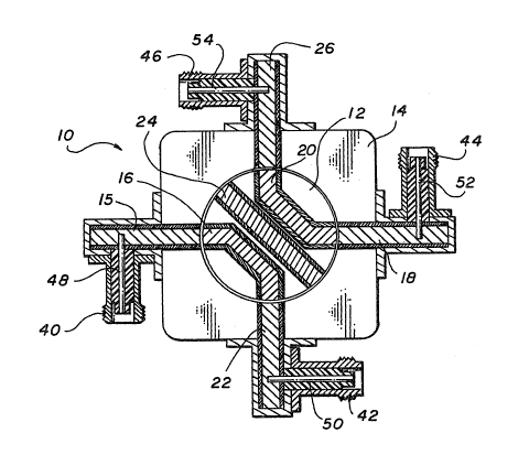
Fig. 2 shows a corresponding illustrative embodiment
; of a dielectrically loaded waveguide switch 10 utilizing
the teachings of the present invention. The switch 10 is
shown in section and includes a rotor 12 which contains a
2~ plurality of dielectrically loaded waveguides 16, 20 and
24 and a stator 14 which contains a plurality of
dielectrically loaded waveguides 15, 18, 22, and 26. The
dielectrically loaded waveguides 15, 16, 18, 20, 22, 24,
and 26 differ from waveguides 15', 16', 18', 20', 22',
30 24' and 26' of the related art in that waveguides lS, 16,
18, 20, 22, 24 and 26 are loaded with a dielectric
material, and dielectrically loaded waveguides 15, 22, 18
and 26 of the present invention differ from waveguides
15', 22', 18' and 26' of the related art in that
35 dielectrically loaded waveguides 15, 22, 18 and 2~ are
' ` , ' ' .. .~.:: ~ , ,,
~ - ~
~zs~als
coupled to coaxial connectors 40, 42, 44, and 46
respectively through coaxial probes 48, S0, 52, and 54
respectively. Note that the size of dielectrically
loaded waveguides 15, 16, 18, 20, 22, 24 and 26 is
reduced rom the size of waveguides 15', 16', 18', 20',
22', 24' and 26' of the related art by the square root of
the dielectric constant (er) of the loading material.
A common low loss dielectric material fabricated
from Barium tetritinate has an er of 37. Using this
dielectric material, the dielectrically loaded waveguides
15, 16, 18, 20, 22, 24 and 26 of the present invention
can be reduced in size to less than one sixth that of
waveguides 15', 16', 18', 20', 22', 24' and 26' of the
related art. The invention is not limited to any
particular size of waveguide or type of dielectric
material. Those skilled in the art having access to the
present teachings will be able to design dielectrically
loaded waveguide switches using dielectric mater~als
suitable for the switch size, and microwave frequency
desired for a particular application.
The rotor 12 is essentially the same as 12' of the
related art except that the size of the rotor 12 can be
substantially reduced due to the reduced size of
waveguides 16, 20 and 24. The stator 14 is essentially
the same as 14' of the related art with the exception
that coaxial connectors 40, 42, 44 and 46 are mounted on
stator 14 and the size of stator 14 is reduced due to the
reduced size o~ dielectrically loaded waveguides lS, 18,
22 and 26. It will be appreciated by those skilled in
30 the art that connectors 40, 42, 44, and 46 may be SMA or
other suitable connectors without departing from the
scope of the present invention. In addition, transitions
to dielectrically loaded waveguides or to standard
waveguides could be used in place of a coaxial connector
without departing from the scope of the present
:
: .~ . . . -
invention.
In operation in the configuration of Fig. 2 and with
the rotor in the position shown, a microwave signal
supplied to coaxial connector 40 will propagate along
coaxial probe 48 and through dielectrically loaded
waveguides 15, 16 and 22 to coaxial probe 50 of coaxial
connector 42 and a microwave signal supplied to coaxial
connector 44 will propagate along coaxial probe 52 and
through dielectrically loaded waveguides 18, 20, and 26
to coaxial probe 54 of coaxial connector 46. It should be
noted that the above illustration is only an example of a
possible configuration. Similarly, by rotating rotor 12,
different dielectrically loaded waveguides will be
aligned, to allow a microwave signal to propagate in
either direction between coaxial probes of different
coaxial connectors. It will be appreciated by those
skilled in the art that the configuration of the switch
and the number of waveguides may vary without departing
from the scope of the present invention.
While the present invention has been described
herein with reference to an illustrative embodiment and a
particular application, it is understood that the
invention is not limited thereto. Those having ordinary
skill in the art and access to the teachings of the
present invention will recognize additional modifications
and applications within the scope thereof.
For example, the present invention is not limited to
switches. Instead it may be used wherever it is desired
to reduce the size of a waveguide. In addition, the
present invention allows for a variety of system
configurations by which waveguides are switched.
It is there~ore intended by the appended clai~s to
cover any and all such modifications, applications and
embodiments.
,~