Note: Descriptions are shown in the official language in which they were submitted.
1.?~334
r
E~ACKGROUND OF THE INvENTlON
The present invention relates generally to digital
data processing, and more particularly to an improved digital
data separator.
Digital data is conventionally stored on a floppy disk
in one of several codes or formats. Self-clocking Manchester
codes (FM, MF~, Biphase, M~F~, RLL 2,7 and the like) are widely
used in data stored on disks, particularly in magnetiC storage
and data communications. The data coded in accordance with
these and other codes contains both cloc~ and data information
in a Common data stream. In order to utilize the data from the
disk, a data separator is typically provided to separate the
data from the clock and to provide separate data and clock
signals for use by an external utilization device, such as a
disk controller.
Because of the noise and jitter that typically occur
in the data stream from the disk, and possible variations in
the rotational speed of the floppy dis~, the data separator
must also be able to maintain synchronization between the
reconstructed reference clock and the input data and to make
necessary adjustments in the reference clock for variations in
the frequency or period of the input data received from the
dis~ so as to maintain the regenerated data pulse in the middle
of a half bit cell or data window. One widely used technique
for separating data and developing a reference clock from the
encoded data stream involves the Use Of an analoq phase-locked
loop. The an~log circuits used in an analog phase-locked loop,
however, are generally more expensive and less reliable than
digital circuitry. For this reason attempts have been made in
recent years to implement phase-locked loops for use in data
334
separators that employ digital circuits and techniques. One
prior approach to the digital implementation o a phase-locked
loop is described in U.S. Patent No. 4,472,818, which issued to
John M. Zapisek and is assigned to the assignee of the present
application.
Although the known digital data separators, sùch as
the one described in the aforesaid patent, have proven to be
successful in many applications, they generally require high
clock rates in order to achieve acceptable performance,
particularly with reSpeCt to accuraCy and resolution. As a
consequence Of the requirement Of a high clock rate, it is
generally not cost effective to implement these known digital
data separators in MOS integrated circuits. In addition, some
of the known digital data separators compromise performance,
such as bit jitter tolerance, to allow them to operate at a
lower clock rate.
The conventional digital data separators typically
correct the data in the data window to a best-case resolution
of plus or minus one operating clock period. For this reason,
the more accurate digital data separators employ both
short-term (phase) and long-term (period) corrections to the
data in order to achieve acceptable aCcuraCy. The phase
correction compensates for relatively fast data window
distortions (suCh aS bit jitter), whereas the period correction
compensates for slow distortions (such as motor speed
variation). Each of these corrections attempts to place the
separated data pulse in the middle of the correct data window,
These techniques, however, have several drawbacks relating to
the slow clock speeds and the resultant poor resolution.
1i29 ~;L 3 3 L~
~0538-9~1
time-weighted previous period data, and also includes a
~ractional period accu~ulator that provides a carry signal to
the counter to improve resolution o:E the counter without
~equiri~g a higher operating clock.
To SummariZe, the present invention provides a
digital data sep~rator for deriving separated data and clock
signals from an input encoded data stream that includes data
and clock pulses, sald data separator co~prising a source of
clock pulses, means for synchronizing each input data pulse
with one of said clock pulses to generate synchronized data
pulses, a counter coupled to said clock source, the count in
said ~ounter being incremented by said clock pulses until its
~ount equals a predetermlned period, latch ~eans coupled to
said counter and effective upon the receipt of one of said
synchroni~ed data pulses to store therein the value of said
counter, said count value representing the required period
adjustment, signal means coupled to sald latch means for
digitally processing said period adjustment signal and for
derlving a digital signal representing the previous period,
comparator and logic means having first and second inputs
operatively respectively coupled to the outputs o~ said counter
and said processing means for produclng a reference clock
signal when the output of said counter is a present ration of
said previous period signal, and a data regeneration circuit
operatively coupled to the output of said comparator and logic
means for generating separate data and clock signals in
response to said reference clock signal and synchronized data
signals.
BRI~F DFSCRIPTION OF TH~ DRAWING5
To the accomplishment of the above and sych further
objects as may hereinafter appear, the present invention
relates to a digital data separator substantially as defined in
.~.,
~94334
SUMMA~Y OF THE INVEN~IQ~
It is an object of the present invention to provide a
digital data separator that resolves the problems preSent in
the operation of the known data separators and which provides
increased resolution and accuracy without requiring a
correspondingly higher operating clock rate.
It is a further object of the present invention to
provide a digital data separator which simulates the operation
of an analog phase-locked loop.
It is another object of the present invention to
provide a digital data separator of the type described that
requires no external components and can operate reliably over a
wide range of input data rates.
It is yet a further object of the present invention to
provide a digital data separator which obviates the need for
short-term correction for all but the highest data rates.
To these ends, the present invention provides a
digital data separator which achieves improved resolution of
the period correction by the use of a digital phase locked-loop
that develops a period value for the reference clock that is
incrementally modified in accordance with the new input data so
aS to position the regenerated data pulse in the middle of the
data window or half bit cell. The digital phase-locked loop
includes a zero-crossing oscillator including an up-down
counter that is incremented by an internal clock until its
output is equal to the normal period of the half bit cell. The
count value in the up-down counter is latched by the next
synchronized input data pulse and represents the value of the
required period adjustment. The phase-locked loop circuit
~urther includes a normal period adjuster and a di~ital
low-pass filter that includes a memory element to remodel the
~Z9~334
6053~-9~1
the appended claims and as described in the following detailed
specification, as considered in conjunction w~th the
accompanying drawings in which:
FIGURE 1 is a schematic block diagram of a digital
data separator in accordance wit,h an embodiment of the present
invention;
FIGURE 2 is a schematic diagram of the half-bit data
synchronizer of the data separator of Fig. l;
FIGURE 3 is a schematic diagram of the zero-crossing
counter oscillator of the data separator of Fig. 1;
FIGURE 4 is a schematic diagram of the fraction
period accumulator of the data separator of Fig. 1;
FIGUR~ 5 is a schematic diagram of the linear
converging low-pass filter of the data separa~or of Fig. 1;
FIGURE 6 is a schematic diagram of the f inite phase
corrector of the data separator of Fig. 1;
FIGURE 7 ls a schematic diagram of the normal period
adjuster of the data separator of Fig. 1;
FIGURE 8 is a schematic diagram of the data
regenerator of the data separator of Fig. 1;
-- ~ 4a
3~4
FIGURES 9(a)-(c) are timing diagrams of the input
signal and re~erence clock to provide a better understanding of
the operation of the data separator of the invention; and
FIGURES lO(a) and lO(b) are waveforms o~ the normal
period value ~PBUS) signals for use in understanding the
operation of the data separator o~ the invention.
DETAILED DESCRIPTION OF THE DRAWINGS
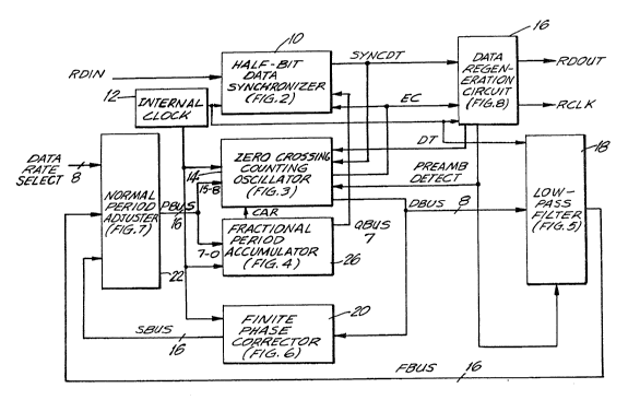
The data separator of the present invention, as in the
embodiment illustrated in Fig. 1, receives an encoded input
data stream RDIN, such as from a floppy disk, at the input of a
half-bit data synchronizer 10. The data may be encoded in one
of the several Manchester codes and, as is per se conventional,
includes both clock and data pulses in a common data stream.
AS described in greater detail with reference to Fig. 2, data
synchronizer 10 generates a synchronized data SYNCDT pulse
which is synchronous with an internal or master cIock 12 for
each data pulse from RDIN detected at the input of the data
synchronizer.
The SYNCDT pulse is applied as one input to a
zero-crossing counter oscillator 14, which, as described in
greater detail in Fig. 3, generates an end count or reference
clock signal EC, which along with the SYNCDT pulse, is applied
to an input of a data regeneration circuit 16, described in
greater detail below with reference to Fig. 8. The re~erence
clock signal EC is also applied as an input to data
synchronizer 10.
~9~3~34
Data regeneration circuit 16 generates the desired
separated and synchronized data RDOUT and clock signals RCLK
from the EC and SYNCDT signals, as explained below. Data
regeneration circuit 16 also generates a data signal DT and a
preamble detect signal PREAMB DETECT, which are applied as
inputs to Counter oscillator 14.
As described in greater detail below, counter
oscillator 14 includes an up-down counter that is incremented
by the internal clock until its output is equal to the normal
period of the half-bit cell. The SYNCDT signal received from
the data synchronizer 1~ latches the Counter ~alue to provide a
count or period adjust signal DBUS to a digital low-pass filter
18. The value of the DBUS signal, which represents the
required period adjustment, approaches zero as the Counter in
counter oscillator 14 synchronizes with the relatively constant
period input data. The PREAMB DETECT signal from data
regeneration circuit 16 is also applied to low-pass filter 18.
Low-pass filter 18 and phase corrector 20 are described in
greater detail in Figs. 5 and 6, respectively.
As also described in greater detail below, the digital
low-pass filter 18 adds the period adjustment value (DBUS) from
counter oscillator 14 to a value stored therein for every input
data transition. This stored value represents a weighted
average period value that, in effect, remembers previous
adjustments made to the period in a manner similar to an analog
low-pass filter. The stored value will converge or decrease to
zero over time if no input transitions occur. The function of
the low-pass filter 18 is to ensure that the normal period of
the half-bit cell will contain weighted components provided by
33~
the previous period adjustments. 'rhe function of the phase
corrector 20 is to provide phase correction to input data when
required, such as when the data rate is high.
The FBUS output of the low-pass filter 18 and the SBUS
output of the finite phase corrector 20 are applied as inputs
to a clamped normal period adjuster 22, which is described in
greater detail below with reference to Fig. 7. The output of
the low-pass filter 18 is added to a programmable input value,
the Data Rate Select, in the normal period adjuster 22. The
programmability of the value of the Data Rate Select signal
allows one hardware implementation of the data separator to
operate at different input data rates. In effect, the Data
Rate signal determines the coarse component, whereas the FBUS
signal obtained from the low-pass filter 18 determine the fine
component of the normal period of the half-~it cell.
The normal period adjuster 22 generates a PBUS signal
which is applied as an input to counter oscillator 14 in which
the PsUS signal, as described below, is used to set the range
of the counter in counter oscillator 14. The PBUS signal is
also applied as an input to a fractional period accumulator 24,
which, as described below with respect to Fig. 4, generates a
carry out signal CAR that is applied to counter oscillator 14
to increase the resolution of the latter without requiring a
higher operating clock. Fractional period accumulator 26 also
generates a QBUS signal, the most significant bit (MSB~ of which is
applied as an input to the half bit data synchronizer 10.
Broadly considered, in the data separator of Fig. 1,
counter oscillator 14, low~pass filter 18, and normal period
adjuster 22 make up a diqital implementation of an analog
phase-locked loop in which the end of count output or re~erence
clock EC of counter oscillator 14 corresponds to the output of
~ 9 43~
a voltage-controlled oscillator and the DBUS data generated by
counter oscillator 14 corresponds to the phase error output Of
the phase comparator in an analog phase-locked loop.
Thus, as shown in Fig. 9(a), when the reference clock
EC is synchronized with the input data, as is desired, the
value of DBUS is zero. However, whenever there is a variation
in the frequency (or period) of the input data, such as to
cause the reference clock to become unsynchronized with the
input data, the value of DBUS is modified in counter oscillator
14 to cause an adjustment in the relative position of reference
clock EC, thereby to cause the latter to become aligned or
synchronized with the input data and the value of D8US to
oscillate and incrementally move toward zero at which time
synchronization will be again achieved betweén the reference
clock and input data as desired, as shown in Figs. 9(b) and (c).
Half-Bit Data Svnchronizer 10
The half-bit data synchronizer 10 receives the input
data RDIN at the clock input of a flip-flop 30, which converts
the rising edge of the RDIN signal to level form. ~he Q
terminal of flip-flop 30 is connected to its D terminal and to
the D terminal of a flip-flop 32, which delays the signal by
one-half clock. The Q output of f lip-f lop 30 and the Q
terminal of flip-flop 32 are connected respectively to the O
and 1 inputs of a multiplexer 34.
The output of multiplexer 34, which is either the
normal or delayed data, is applied to a level change detector
made up of flip-flops 36 and 38 and exclusi~e OR gate 40, the
inputs of which are respectively connected to the Q terminals
of the flip-f lops 36 and 38. The output gate 40 is the
synchronized data single SYNCDT.
12~334
The control signal for the multiple~er 34 is derived
from QBUS7 the most significant bit (MS~) of the signal
produced in fractional period accumulator 26. The true and
inverted values of the QBUS7 signal are respectively applied to
one inpUt Of each of AND gates 42 and 44, which receive the
reference clock EC at their other input. The outputs of gates
42 and 44 are respectively applied to the ~ and K terminals of
a flip-flop 46. The output of flip-flop 46 at its Q terminal
is the control signal for multiplexer 34.
This arrangement will cause the synchronized data
SYNCDT to move back and forth by half a clock according to the
truncated size (to the half clock) of each half bit cell. In
effect, thiS permitS half-bit cell window resolution with half
clock accuracy without increasing the clock rate.
Zero-Crossina Counter Oscillator 14
The input to the zero-Crossing Counter oscillator 14
is made up of bits 15-8 of PBUS, which, as descri~ed below, is
the modified or adjusted value of the D~US signal produced by
the counter oscillator 14. This 8-bit signal is stored in a
register incrementer 48 to which may be added the carry signal
CAR derived, as described below, in the fractional period
accumulator 26. The adjusted PBUS signal, designated QBUS, is
applied for each half bit to a register 50. The output of
register 50, which represents the digital value of the present
period (PPV), is applied to an inverting input of a multiplexer
52 and to a divide-by-two CirCuit 54. The output of the latter
is decremented in a de~rementer 55 by the PREDT signal from the
output of AND gate 57. The output of divider 54 is applied to
one input of a comparator 56.
g
l~g~33~
The output of multiplexer 52 is applied to ~
divide-by-2 circuit 60. The output of the latter is applied to
a zero-crosslng coUnter 58, which is preferably in the form Of
an 8-bit binary up-down counter. The output of counter 58 is
applied to the other input of comparator 56 and back to the
other (non-inverting) input of multiplexer 52. The output of
the counter 58 is also applied to a decoder circuit 6z the
output of whiCh goes active (high) when the Counter output
equals 2.The count = 2 output is applied to one input of a NAND
gate 64, the output of which is applied to the clear CLR input
Of counter 58. The other input to gate 64 is the inverted bit
8 of the signal from register 50. The output of the counter 58
is captured in latch circuit 66, which is triggered by the
SYNCDT signal from data synchronizer 10. That signal is also
applied to one input of an AND gate 68, which also receives the
PREAMB DETECT signal as does the other input to AND gate 57.
The output of gate 68, which is the PRESYNCDT signal,
iS applied aS the control signal for multiplexer 52, and to one
input of a NOR gate 70. The other input to gate 70 is the
reference cloc~ EC. The output of gate 70 is applied to the LD
tload) input of counter 58. The value of bits 15-8 of the P~US
signal produced by the normal period adjuster 22 is the integer
part of the desired or nominal period of the half-bit cPll.
This value may or may not be incremented dependent on the value
of the carry signal CAR from the fractional period accumulator
26, which prevents the loss of the fractional portion of the
period value. This value of PBUS is transferred into register
50 each half bit cell. This value, which is stored in register
S0 and represents the present period value, is applied to
counter 58 through multiplexer 52 when the EC signal is
generated and is effective to directly control the period of
-- ~0 --
~LZ~3;}4
the counter during normal operation, that is, when the
PRESYNCDT signal is not active.
In a preferred embodiment, counter 58 counts in 2's
complement notation from -12a to ~127 in increments of 1 for
each input clock pulse until it is loaded by the end count
signal EC or during sync detect by the PRESYNCDT signal at the
output of NOR gate 70. Counter 58 then proceeds to increment
from this newly loaded value.
The end count signal EC is produced by co~parator 56
when its two inputs are equal, that is, when the output of the
counter 58 is equal to one half the output of register 50, the
present period value or one half the bit cell. This value is
generated by shifting down (dividing by two) the output of the
register 50 and possibly decrementing by 1. At that time
counter 58 is preloaded with the value of l/2 the present
period value (PPv) by inverting at the input of the multiplexer
and shifting down the value in register 50.
A zero-crossing counter (ZCC) is preferably used as
the counter 58 because the zero count is located in the middle
part of the Counter's Counting sequence. This allows a 50 per
cent correction to ~e made by a one-bit shift downward in the
count in the counter. Ideally, counter 58 should be
symmetrical about Zero. As shown in the following example,
this may be accomplished by simulating the behavior of a two's
complement counter through the use of a count =2 decoder 62.
The resultant counting sequence is then normalized by the
normal period adjuster 22 to yield the required continuous
counting sequence that is symmetrical about zero.
EXAMPLE lA: Zero=Crossing Counter Oscillator Count =8
PPV = o o 9 o o o
PPV Inverted = 1 1 1 1 1 1 0 0 0
PPV Inverted/2 = 1 1 1 1 1 1 1 0 0
PPV/2 ZCC Counting Sequence EC
O O O O O 0 1 1 1 1 1 1 1 1 0 0 0
1 1 1 1 1 1 0 1 0
1 1 1 1 1 1 1 0 0
1 1 1 1 1 1 1 1 0
O O O O O O O O O
O O O O O O 0 1 0
V O O O O O 0 1 0 0
O O OO O 0 1 1 0 0 0 0 0 0 1 1
1 1 1 1 1 1 0 0 0
The resulting count is asymmetrical a~out zero with
four negative counts and three positive counts. The
counting sequence is normalized in the normal period
adjuster 22 where the:
-4, -3, -2, -1, o, 1, 2, 3
sequence is converted to:
-3, -2, -1, 0, O, 1, 2, 3
EXAMPLE lb: Zero- Crossing Counter Oscillator Count = 7
PPV = O O O O 0 1 1 0
PPV Inverted = 1 1 1 1 1 0 0 1
PPV Inverted/2 = 1 1 1 1 1 1 0 0
- 12 -
1;~94334
PPV/2 ZCC Counting Sequence EC
O o o o o o 1 1 1 1 1 1 1 1 0 0 0
1 1 1 1 1 1 0 1 0
1 1 1 1 1 1 1 0 0
O o o o o o o o o
O O O O O o o 1 0
V O O O O O 0 1 0 0
O O o o o o 1 1 o o o o o o 1 1
1 1 1 1 1 1 0 0 0
AS shown by this example, the -2 count is skipped when
the output of decoder 62 iS aCtive high and the LSB of
register 50 is low. The resulting count is
symmetrical about zero with three negative counts and
three positive counts. The counting sequence is
normalized in the normal period adjuster 22 where the:
-4, -3, -2, O, 1, 2, 3
sequence is converted to:
-3, -2, -1, O, 1, 2, 3
An additional reason for the use of a zero-crossing
counter is to allow for instant phase error detection
implementation. AS shown in Fig. 3, the synchronized read data
signal SYNCDT applied to the clock input of latch 66 causes the
latter to latch the value stored in counter 58, which is
already in 2's complement form. This latched data, which is
the error signal D8US, is latched upon the receipt of a
synchronized input data SYNCDT at the clock terminal of latch
66, and the DBUS error signal is then ready for period or-
additional phase CorreCtion as described below.
129433~
The PREDT and PRESYNDT signals work together and allow
the ZCC to make an i~mediate and large phase CorreC~ion when
the PREAMB DETECT signal is active (ie. when the data SYNC
field has been detected in the data regeneration circuit 16.
PRESYNCDT
__________________________________.____________________________
-7 -6 -5 -4 -3 -2 -l O 1 2 3 4 5 6 7
_______________________________________________________________
ZCC COUNTER (OLD)
v
______________________________________________________
-7 -6 -6 -4 -3 -2 -1 0 1 2 3 4 5
______________________________________________________
ZCC COUNTER (NEW)
v
________________ _____________________________________
-6 -5 -4 -3 -2 -l 0 l 2 3 4 5
______________________________________________________
ZCC COUNTER (EFFECTIVE)
The PRESYNCDT data signal, which controls the
operation of the multiplexer 52 and loads the counter 58, is
generated by ~ND gate 68. The PRESYNCDT signal will cause
counter 58 to immediately load hal~ of its present value
through multiplexer 52. As shown in the diagram above, this
will cause an immediate 50 percent phase correction to counter
58 changing the count from ZCC counter (old) to ZCC counter
-- 14 --
._ .
~;~9~334
(new). The loading of counter 58 requires one clock cycle. In
this example, the uncorrected counter 58 would have advanced to
the count of 5 during this clock cycle. To operate correctly,
the new divided by two value of counter 58 has to be
incremented by one to compensate for the lost clock cycle. The
present implementation effectively increments the count value
by generating the EC signal one clock early. The EC signal is
generated earlier because the one half present period value
generated by divide-by-two circuit 54 is decremented in
decrementer 55 by the PREDT signal obtained from AND gate 57
yielding the ZCC counter (effective) value.
In the present implementation, divide-by-two circuits
54 and 60 are constructed with binary shift registers. The
phase corrections that result for both the case when QBUS bit
8, the LSB from register 5~, is zero (~BUS even) or one (PBUS
odd ) a re:
QBUS even
counter 58 value: -4 -3 -2 -1 0 1 2 3
next value: -2 -2 -1 -1 0 0
effective correction +2 +1 +1 0 0 -1 -1 -2
QBUS odd:
counter 58 value -4 -3 -2 o 1 2 3
next value: -2 -2 ~0) 0 0
effective correction: +2 +1 +1 o -1 -1 -2
note: () by reset via NAND qate 64
From the foregoing, it can be understood that if the
received data pulse is centered in the data window or half bit
cell, as defined by the EC signal produced by comparator 56,
:1~94~34
the value in counter 58 and in latch 66 will be zero when the
SYNCDT signal is ~enerated. If the data pulse is moved away
from the center of the data window as a result, for example, of
jitter or a change in motor speed, the value in the counter 58
will be greater than or less then zero by an amount
proportional to the variation in the input data pulse. That
value as latched into latch 66 is the DBUS signal which
represents the error in the position Of the input data pulse.
This value will be used in determining the correction to the EC
reference clock that is required, as shown in Figures 9a, gb,
and 9c.
Fraction Period Accumulator 26
As shown in Fig. 1, the fractional part of the normal
period value (PBUS bits 7-0) is applied to the input of the
fraction period accumulator 26. As shown in Fig. 4, those bits
are applied to one input of an adder 72. The output of adder
72 iS applied to a regiSter 74 and the register output is
connected back to the other input of the adder.
The output of the adder 72 is the carry signal CAR
which, as noted above, is applied to the incrementer 48 in
counter oscillator 14 to increment the integer part (bits 15-8)
of the present period value that is latched into register 50 by
1 when the CAR signal occurs.
This logic allows a greater resolution of the present
period value than would otherwise be obtainable at the
operating clock rate. For example, if, as in the embodiment
herein described, 8 bits are chosen for f raction period
computation, the logic system consistin~ of the counter 5B and
the fraction period accumulator 26 has the ability to count the
1~34334
desired period value with a maximum phase error of ons clock
over a maximum of 16 bytes (Z56 half bit cell times). If no
fractional period accumulator was used, the counter 58,
register 50, comparator 58 and other associated logic in the
zero crossing Counter oscillator 14 would have to operate on a
bigger word (greater than 8 bits). The use of the functional
period accumulator allows the required accuracy with only an 8-
bit counter. If a larger counter were used, the operating
frequency would have to be increased to allow the wider counter
to reach its full range in the bit cell time. The most
significant bit ~MSB) of the output of the r~gister 74 is the
QBUS7 signal, which, as noted above, is applied to the data
synchronizer 10.
Linear Conver~inq Low-Pass Filter 18
The DBUS error signal is applied to the low-pass
filter 18, illustrated in Fig. 5, which operates on the DBUS
signal in a manner that is analogous to that of an analogue
iow-pass filter in an analog phase-locked loop. AS shown in
Fig. 5, the bits of the DBUS signal from the counter oscillator
14 are applied as inputs to a multiplexer 76 which is
controlled by the PREAMB DETECT signal obtained from the data
regeneration circuit 16.
The DBUS signal iS passed through mutliplexer 76 to
the inputs of an adder 78, the output of which is applied to a
register 80. The output of register 80, which is the Fsus
siqnal, is applied to one input of a subtractor 82 and to an
inverting input of the subtractor through a divide-by-four
circuit 84. The output of the subtractor 82 is applied to the
other input of the adder 78. The borrow signal to the
- 17 -
lZ~3~3~4
subtractor is obtained from a multiplexer 86, which receives
inputs from NAND gate 88 and NOR gate g0, which, in turn,
receive the least significant bits of the FBUS signal at their
other inputs. If F~US is a negative number (the MSBzl) then
multiplexer 86 passes the output of NAND gate 90 to the BI
(sorrow In) input of subtractor 82. If FguS is positive (the
MSB=0) then multiplexer 86 passes the output of NOR-gate 88 to
the BI input o~ subtractor ~2. This will cause the output Of
subtractor 82 to converge to zero for Fsus positive and -1 for
FBUS negative (-1 will be changed to zero as described in the
normal period adjuster 22.)
It will be understood that the value of FBUS stored in
register 80 can be made to converge to zero by subtracting a
fixed percentage of itself for each half bit cell. Stated
differently, the value stored in register 80 ~ill have what may
be considered a "time" effect (i.e., over a series of bit
cells) on the CompUtation of the value Of the period. To this
end, 1/4 of the value stores in register 80 is subtracted from
itself in subtractor 82 and applied to one input of adder 78.
The value of the DBUS signal, through the gain control
multiplexer 76, is added to the processed value applied to the
other input o~ Adder 78 and for each transition in a bit cell;
there is no addition if there iS no data transition in the bit
cell.
Finite Phase Corrector 20
Finite phase corrector 20, aS shown in Fig. 6,
receives the DBUS signal and passes it through a
divide-by-eight circuit 92 and a divide-by-two circuit 94. The
outputs of circuits 92 and 94 are summed in an adder 96 and
- 18 -
4334
passed to a register 98. The output of register 98 is the S8US
signal, which is applied as one input to the normal period
adjuster 22.
Finite phase corrector 20 may be included in the data
separator of the invention to perform minor phase correction
for each data transition in order to keep in synchronization
with the input data. If no finite phase correction is needed
the value o~ S8US may be forced to zero. For low data rates
the outpUt of finite phase corrector 20 will approach zero.
Normal Period Adiuster 22
The normal period adjuster 22, as illustrated in Fig.
7, receives the FBUS signal from the low pass filter 18 at one
input of an adder 100 and the SBUS signal from the finite phase
corrector 20 at one input of an adder 102. The output of adder
100 is added to the other input of adder 102 and applied to the
input of register 104, the output of which is applied to the
other input of adder 100.
The two MSB outputs of adder 102 are applied to the
inputs of a multiplexer 106. The remaining outputs of adder
102 and the output of multiplexer 106 are applied to the input
of an adder 108, the output of which is the F8US or normal
period signal. The other inpUt to adder 108 is a Data Rate
Select signal, one bit of which is also applied as the control
signal to multiplexer 106. The Data Rate Select signal is a
binary signal programmed by the user that represents the rate
o the input data to the data separator.
It will be understood that the F~US siqnal represents
the filtered immediate period variation which increases or-
decreases the period conversion value stored in register 104
-- 19 --
~Z~433~
every half bit cell. The normal period value F8US is thus the
sum of the Data Rate Select, FBUS and Ssus signals, as shonw in
Figs lOa and b.
The values of the two MSBs at the output of adder 102
are applied to multiplexer 106. The output o multiplexer 106
is applied to the input of adder 108 such that multiplexer 106
provides hardware control, as shown, so that the value at this
input of adder 108 will not be greater than +/- a predetermined
number, which typically would be ~/- 6 per cent o~ the
progra~med data rate. This will prevent the digital phaselock
loop from overreacting at extreme condi~ions, such as power-on
or reading with noisy data, which could cause the unclamped
phase-locked loop out of its lock range.
As can be seen in Fig. 7, and as described in the
description o zero-crossing counter oscillator 14, the
difference or error value DBUS derived from the zero crossing
counter oscillator 14 is compensated in the normal period
adjuster 22 by tying the carry in of adder 100 to the most
significant bit (MSB) of the F~US signal. This arrangement
causes all negative numbers to ~e incremented by 1, which, in
turn, reæults in a phase value symetrical about zero. A
similar circuit is, as shown, employed in the carry in of adder
102 for SBUS value mapping.
Data Reaeneration Circ~it 16
The data regeneration circuit 16, as shown in Fig. 8,
receives the SYNCDT signal from the data synchronizer 10 at the
input of a flip-f lop 110 . ~he SYNCDT signal is also inverted
in an inverter 112 and applied to one input o an AND gate
114. The end count signal EC is applied to the othe~ input of
- 20 -
lZ~433~
AND gate 114 and to the load/shift input of a shift register
116. The output of AND gate 114 is applied to the K input of
flip-flop 110. The Q output of the last stage of the shift
register 116 is the regenerated data signal RDOUT.
The end count signal EC is also applied to one input
of AND gates 118 and 120 and to the EN inputs of fllp-flops 122
and 124. The output of AND gates 11~ and 120 are respectively
applied to the J and K inputs of a flip-flop 126. The output
at the Q terminal o~ flip-flop 126, which is the regenerated
clock RCLK, is connected to the second input of AND gate 120,
whereas the inverted output at the Q terminal is connected to
the second input of AND gate 118.
The signal at the Q terminal of flip-flop 110 iS the
DT data signal, which is applied to the counter oscillator 14
and also to the D input of two-bit shift register 122. The
outputs at the Ql and Q2 terminals shift register 122 are
connected to the inputs of an e~clusive-NOR gate 130, the
output of which is applied to one input of an AND gate 1~2.
The output at the Ql terminal of two-bit shift
register 12g iS connected to one input of an AND gate 134,
which receives at its other input the inverted output of the Q2
terminal shift register 124. The output of AND gate 134 is
applied to one input of an OR gate 138 and to the Sl input of a
shift register 140. The end count si~nal EC is applied to a
third input of AND gate 134 and to one input of AND gate 142,
the output of which is applied to the second input of OR gate
138. A read gate RG signal is applied to the D input of
flip-flop 124 and to the clear C input of shift register 140.
The output of the Qa terminal of shift register 140 is
applied to a second input of AND gate 132, which also receives
lZ 9~ 334
the end count si~nal EC at its third input. The output of AND
gate 132 is applied to the Sl terminal of a shift register 144,
which further receives the end count signal ~C at its 50
terminal. The Qb output of register 140 constitute the PREAMB
DETECT s i g nal.
The output stages of Shift regiSter 144 are connected,
as shown in Fig. 8, to the inputs of NOR gates 146-and 148 and
an AND gate 150. ~he outputs of these gates are applied as the
inpUtS to a NOR gate 152, the output of which is connected to
the R terminal of shift register 144. The output of NOR gate
148 is connected to the second input of AND gate 142.
In operation, the data reqeneration circuit 16
generates the read clock RCLK and read data RDOUT signals from
the synchronized RDIN data (SYNCDT) and the end Count or
reference clock signal ~C. The data generation shift register
116 places a RDOUT pulse in the middle of a RCLK window when
the EC signal loads regiSter 116 after the SYNCDT signal has
forced the DT signal high.
The logic portion of the data regeneration circuit
that performs the PREAMB DETECT function looks for a series of
equally spaced SYNCDT pulses when input read gate RG signal is
high. When RG is low, Shift register 140 will be held in the
reset condition. The transition of RG from low to hiqh will
parallel load shift register 140, thereby to cause the Preamble
Detect signal to go to zero.
When the Qa output of register 140 goes high it
enables the initialization of the random walk counter composed
of shit register 144, NOR gates 146, 148, 152, and AND gate
150, which is then held in the parallel load state until the
output of exclusive-NOR gate 130 goes low. Shift register 122
outputs will cause gate 130 to go low when a steady OOH data
- 22 -
~l2~339~
pattern, such as the disk vCo sync field, resulting in an
alternating 1, 0 RDOUT pattern, is encountered. This will
allow shift register 144 to increment once for each EC pulse.
Shift register 144 will reach its terminal count after it
receives 18 EC pulses if no data pulses are encountered. Shift
register 144 will then allow register 140 to shift and therebY
cause the PREAMB DETECT signal to go high.
- ~3 -