Note: Descriptions are shown in the official language in which they were submitted.
12943~0
- 1 -
~Iigh Speed Quantum Well Optical Detector
This invention relates to the field of semiconductor devices and, more
particularly, to optoelectronic semiconductor devices employing quantum well
layers.
S Backgrou~d Q~ Inventio~
Single and multiple quantum well layer structures have become
increasingly important in the areas of optical communication systems and
optical computing systems. These structures exhibit linear and nonlinear
properties which permit them to be used as logic elements in switching system
10 applications as well as modulation, detection and gain elements in
communication system applications. See, for example, U. S. Patents 4,525,687
and 4,546,244.
In general, these device structures operate on an absorption principle.
That is, the device is illuminated by a light beam from an external source at an15 optical wavelength at or above the absorption edge of the quantum wells. By
electrically manipulating the absorption edge of the quantum well material, it is
possible to absorb or transmit the light incident on the device. When the light
is absorbed in the quantum wells, a voltage may be generated by the
photovoltaic effect. Absorbed photons generate mobile charge carriers that
20 move under the action of an applied electric field. Movement of the charge
carriers changes the electric field and, thereby, generates a change in voltage.This mode of operation is useful in generating a steady current provided that
the light is selected to have a wavelength that is strongly and continuously
absorbed by the quantum wells, i. e., the photon energy of the incident light is25 at or above the bandgap energy of the quantum wells. While this mode of
device operation is useful for detecting relatively long optical signal pulses, it
severely limits the applicability of the device to very high speed optical pulsedetection, among other things, because of the persistence of the absorption
induced photovoltage long after the extinction of a high speed (short) optical
30 signal pulse.
~b
12~3XO
Summarv of the Invention
In response to ultrafast oplical signal pulses, it is now possible to generate correspondinsly
ultrafast electrical signal pulses (~IOOfs) by employing semiconductor apparatus including at least one
quantum well layer electrically biased by a static electric field. ~ptical signal pulses incident on the
quantum well are at a waveléngth substantially less than the absorption edge of the quantum well
material. In other words, the incident optical pulses have a mean photon energy less than the ban(
gap energy of the quantum well layer or layers. A significant fraction of the electrical si~nal pulse
generated subsists for a period of time substantially equal to the duration of the optical signal pulses
incident on the quantum well layer or layers.
According to one aspect of the invention there is provided semiconductor apparatus including
at least one semiconductor quantum well layer, means for applying an electrical potential to said at
least one semiconductor quantum well layer, and a source of an optical signal, said semiconductor
apparatus characterized in that the mean photon energy of said optical signal is less than the band gap
energy of said at least one semiconductor quantum well layer, and said at least one semiconductor
quantum well layer is responsive to said optical signal to induce a change in the electric fielcl there
across, the change of said electric field subsisting for a period substantially equal lo the duration of
said optical signal.
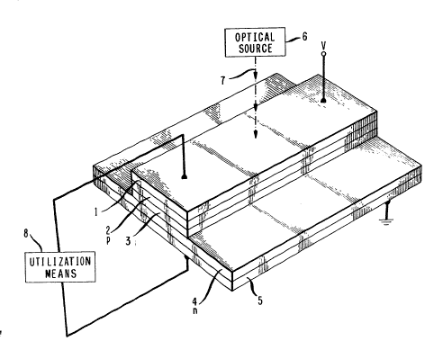
Brief Description of the Drawin~
A more complete understanding of the invention may be obtained by rea~ing the following
description of a specific illustrative embodiment of the invention in conjunction with the appende~l
drawing in which FIG. 1 is a system diagram of semiconductor apparatus in accordance with the
principles of the invention.
Detailed Description
FIG, 1 shows one embodiment of the inven~ion in which an optical signal is incident upon at
least one semiconductor quantum well layer for generating a change in the resulting electric field. In
general, a bias field is applied perpendicular to the quantum well layer or layers. The incklent optical
signal may enter the quantum well or wells from any direction and in any polari~alion provided that
the optical signal can propagate in the quantum well or wells, It should be noted that the
0 semicondutor device shown in FIG. l is not drawn to scale.
In one embodiment, the semiconductor quantum well layer is included in the intrinsic (i) layer
of a p-i-n detector. Electrode l is positioned on an exposed surface of p-type semiconductor layer 2.
It is preferable that electrode 1 be a semi-transparent metallic layer to permit passage of optical signais
incident thereupon. P-type semiconductor layer 2 is positioned on intrinsic layer 3 ~hich includes one
3 5 or more quantum well layers. Intrinsic layer 3 is likewise positioned on n-type semiconductor layer 4.
N-type semiconductor layer 4 is positioned on electrode 5 which is generally fabricated from metallic
12~3~
- 3 -
materials. For the embodiment shown in FIG. 1, electrode 5 serves as a metallic
ground plane and the combination of electrodes 1 and 5 acts as a stripline
transmisssion medium.
In an example from experimental practice, p-type semiconductor layer 2
5 includes p-doped AlGaAs; n-type semiconductor layer 4 includes n-doped
Al(~aAs; and intrinsic layer 3 includes one or more quantum well layers
approximately 100 angstroms thick. In this material system, a sin~le quantum
well layer may include either GaAs or AlGaAs. Multiple quantum well layers in
intrinsic layer 3 may include alternating thin layers of AlC~aAs and GaAs.
10 Semiconductor structures of this type are generally grown by epitaxial growthtechniques described in U. S. Patent Nos. 3,~82,207, 4,205,32s), and 4,261,771 as
well as in the reference book by casey and Panish, "Heterostructure Lasers Part
B: Materials and Operating Characteristics," P~ges 71-155 (Academic Press,
New Yorlc: 15~78).
Optical source 6 generates optical signal 7 at a wavelength below the
wavelength corresponding to the absorption edge of the quantum well layer or
layers in intrinsic layer 3. In other words, the mean photon energy of optical
signal 7 is less than the band gap energy of the quantum well layer or layers inintrinsic layer 3. In an example from experimental practice, optical source 6 is a
20 conventional pulsed dye laser capable of producing an optical signal pulse ofappro~timately 100 pJ of energy and several hundred femtoseconds duration in
an optical spot of area approximately 4,um~.
Utilîzation means 8 is connected to electrodes 1 and 5 of the
semiconductor device to receive electrical signals generated therefrom. In an
25 example from experimental practice, utilization means 8 may be realized as any
electronic or optoelectronic or other sensing device (e.g., transistor or quantum
well device) which is capable of responding to the electrical pulse signals.
For the arrangement shown in FIG. 1, optical signal 7 incident upon
intrinsic layer 3 and having a mean photon energy below the band gap energy of
30 the quantum well in intrinsic layer 3 induces a change of the electric field
perpendicular to the layers 3, 4, and 5. The induced change in electric i~leld
decays instantaneously when the intense optical signal 7 is extinguished,
thereby permitting extremely high speed photo detection. It should be noted
that the p-i-n semiconductor structure shown in FI(:~. 1 is subject to an applied
3~
- 4 -
reversed bias potential of magnitude V volts. As such, optical signal 7 incidenton quantum well layers in intrinsic layer 3 causes corresponding voltage pulses
to propagate on the transmission line formed by electrodes 1` and 5. These
voltage pulses are supplied to utilization means 8.
While it has been shown in FIG. 1 that the electric l`leld is supplied from
an external source, it is now well known that electric fields of sufficient strength
(105 Vlcm) occur in strained layer superlattice quantum wells via piezoelectric
effects and built-in strain mechanisms. See, for example, C. Mailhiot and D. L.
Smith, J. Vac. Sci. Technol. B4, 996 (1~86).
It is expected that the principles of this invention are applicable not only
to the photodetector ;llustrat;vely embod;ed ;n FIC~. 1 but also to other devices
such as optical ;solators, optoelectron;c transducers, and other photonic
switching appl;cat;ons. For example, the device can be used in producing field-
induced four wave mixing. That is, an electric field "grating" created in the
quantum well layer by two interfering optical signals generate a refractive index
grating through quantum confined stark effect electrorefraction and, thereby,
causes scattering of a third optical signal off the grating to generate a fourthoptical signal.