Note: Descriptions are shown in the official language in which they were submitted.
~Z~3~3
-- 1 --
C~RATING COUPLER WITH MONOLITHICALLY
INTEGRATED QUANTUM WELL INDEX MODULATOR
Technical Fieid
This invention involves grating couplers which are used in
5 conjunction with index modulators to affect incident optical radiation.
Specii~lc embodiments of the invention may be used in conjunction with
optical communication systems to process light and/or produce optical
signals encoded in a manner representative of intelligence.
Background of the Invention
The invention of low loss optical i~lbers in the early 1~70s, for use
as a practical optical transmission medium, stimulated explosive growth in
other areas relating to optical communications. So, for example, subsequent
to the development of optical fibers significant effort was directed toward
the development of various optical sources and detectors. The concomitant
15 growth of semiconductor technology led to the development of integrated
sources and/or detectors which could be easily and inexpensively fabricated.
(The term "optical", as used in this application, refers not only to visible
light but to any electromagnetic radiation which can be transmitted
effectively within dielectric fibers, usually with losses less than 2
20 dB/kilometer. Accordingly, the term refers to electromagnetic radiation
generally of wavelength between .1 and 50 microns.)
Along with ad- ances ;n device development, various system
architectures, for use in optical communication systems, have been proposed
and continue to be debated. However, many such systems require a light
25 source which is modulated in a manner representative of intelligence. For
contemplated long haul systems, such light sources must be pulsed as
rapidly as billions of times per second (gigabits/sec). The pulsation may be
in the form of an amplitude pulsation, e.g.,"on" and "off" states, or a
frequency pulsation such as, for example, frequency shift keying in which
30 light of one frequency represents "on" state and light of another frequency
represents the "off" state. Contemplated optical sources must be
considered with a view towards their ability to pulse in such a fashion at
gigabit rates.
~e
~2~3~3
- 2 -
While it is possible to fabricate light sources such as injection
lasers which may be inherently pulsed at gigabit rates by direct current
modulation, such high pulse rates introduce deleterious spectral-broadening
side effects such as "chirp" (T. L. Koch, J. E. Bowers, Electron. Lett., 20,
5 1038 (1~84)). However, such deleterious effects can be reduced if an
external modulator is used to vary the otherwise constant output of a light
source, or an intracavity modulator is used in a laser, thereby yielding
pulsating light representative of intelligence.
In other wavelength division multiplexed ("WDM") applications,
10 it is contemplated that a number of different wavelength channels will be
used in optical tran~mission or switching architectures. For these
applications tunable light sources may be used, or tunable optical filtering
devices might be used, to determine which wavelength channel is
transmitted or received. Such devices can also be used to re-route a given
15 signal within an optical communication netw-~rk. To achieve such
tunability or wavelength channel selection, most devices contemplated
employ me~lia whose index of refraction can be modulated or controlled
within the device to a desired value.
Particularly useful for modulation as described in the foregoing
20 applications are electrooptic devices whose optical properties, such as
absorption or index of refraction, may be varied by application of an
appropriate electrical signal. Exemplary of such electrooptical devices is the
(Juantum well device. (In this specification the term "quantum well" refers
to one or more quantum wells.)
The quantum well comprises one or more alternating layers of
different semiconductor material. The layers alternate between wide
bandgap material and narrow bandgap material. The valence band of the
wide bandgap material is lower in energy than the valence band of the
narrow bandgap material, while the conduction band of the wide bandgap
30 material is higher in energy than the conduction band of the narrow
bandgap material. The electrons and holes that are formed in the "well"
regions, or that migrate to those regions, are confined to the well regions
due to the lower potential energy in these regions. Such devices are called
quantum well devices because for narrow wells, the electron and hole energy
35 levels are altered by quantum effects. In the case of excitonic states,
confinement of the electrons and holes within a thickness, defined by the
12~3~3
narrow bandgap material layer thickness, that is much less than the normal
exciton diameter, makes the exciton binding energy larger without further
increasing the phonon broadening. This, and other consequences of this
"quantum confinement" explains the persistence of the associated
5 resonances to room te~nperature. In addition, the energies of the confined
electrons and holes are increased as a result of the "confinement energy".
One incidental consequence of the quantum confinement is that it removes
the degeneracy in the valence bonds of the semiconductor, resultin~ two
;citon resonances, the "light hole" and the "heavy hole" exciton.
When an electric f~leld is applied perpendicular to the quantum
well layers, the optical absorption edge, including the exciton resonances,
moves to lower photon energies. Normal bulk semiconductors show very
little, if any, shift in absorption edge. The only consequence of applying an
electric fields to a normal bulk semiconductor is the Franz-Keldysh effect
15 which broadens the band edge with comparatively little shift. At low ~lelds
the exciton peaks broaden and disappear. However, unlike the behaviour of
a bulk semiconductor, when perpendicular fields are applied to a quantum
well device the exciton absorption peak remains resolved to high fields.
The preservation of the exciton resonances when perpendicular
20 fields are applied to MQW devices can be explained by considering the
effect of an electrical field on a confined electron hole pair. Normally, the
application of a field results in exciton broadening because of a shortening
of an exciton lifetime due to ionization. However, since the confinelnent of
the electron hole pairs due to the quantum wells precludes exciton
25 ionization, very large fields can be applied without ionization, and therefore
without broadening of the exciton resona~ces. Additionally, and perhaps
more importantly, when the MQW device is considered for use as a
modulator, there is a significant shift in the absorption edge due to the
change in the conflnement energy associated with the application of the
30 electric field and the consequent distortion of the well. This shift in
absorption is thé basis for the MQW as a modulator. Since varying the
applied field can significantly alter the light absorption properties of a
properly biased MQW, light passing through the MQW will be modulated.
While the electrooptic properties of the MQW described above
35 make it particularly appealing as an optical intensity modulator, the high
degree of absorption encountered in the resonance region results in
~Z~3~3
-
-- 4 --
signii~lcant loss of optical energy in both the "on" and the "off" states of themodulator, which is most often undesirable, and in some applications may
be untolerable. Motivated by this concern various workers have
investigated the use of an MQW device as an "index" or "phase" modulator
5 rather than an absorption modulator. The basic Kramers-Kronig
relationship, which governs the interplay between the change in a material's
absorption characteristics and the change in its index of refraction, dictates
that large changes in index of refracticn will be experienced in regions
removed from the absorption edge. Accordingly, the MQW device may be
lO used as a phase or index modulator with reduced associated absorption
losses. utiiizatioll of such an MQW phase modulator in conjunction with a
Fabry-Perot laser was suggested in u.S. Patent 4,525,687, issued to Chemla
et al., at column 14, lines 1-19.
While early lasers were almost exclusively of the Fabry-Perot
15 type cited by Chemla et al., subsequent developments sug~ested lasers with
distributed reflectors, most often fabricated within a waveguiding structure.
U.S. Patent 3,760,2~2 discusses the operation of a distributed feedback
laser. Such a laser is based on the phenomenon of "grating coupling". This
phenomenon is associated with the passage of light through a region of
20 varying transmission properties, periodic in at least one dimension, i.e., a
"grating". The interaction of light with such gratings involves a phase
matching condition which is only satisfled at certain wavelengths. As is well
known by those skilled in the art, wavelengths for which the phase
matching condition is satisfied are given by the different "orders" of grating
25 coupling. When coupling occurs at the longest wavelength ~0 which
satisfies the phase matching condition, the coupling is referred to as "first
order". Other wavelengths which may also satisfy the phase matching
condition, are M where M=2, 3, 4 ... are the higher orders of operation. In
this application the grating is generally considered to be operating in "first
30 order" (M=1) but may operate in higher orders. Representative of such
"gratings" are regions of varying index of refraction or a corrugation in the
boundary between two materials of different index of refraction. When
light passes through such a region it may be either forward or reverse
coupled to other guided waves. Exemplary of such "grating coupling" is the
35 Bragg reflector- a "grating coupler" which reverse couples incoming light to
129~3~3
- 5 -
a "reflected", outgoing, light beam. The Bragg reflector may be fabricated
external to a gain medium resulting in a Distributed Bragg Reflecting (DBR)
laser. A "grating coupler" may also be fabricated as an integral part of the
grain material resulting in a Distributed Feed Back (DFB) laser. The
5 grating coupler in a DFB laser may be viewed heuristically as simply a
reflector which defines the laser cavity. However, rigorous analysis shows
that the coupling in a DFB laser is mos e complicated because of phase
effects. So, for example, the DFB does not lase at the center of the "Bragg
reflection band" but rather near its two first minima.
The quantum well device and the distributed feedback laser
have been combined to yield devices such as quantum well lasers. The
quantum well laser utilizes the electronic properties of the quantum well to
define energy levels which are particularly advantageous for use as laser
transitions .
15 Summary of the Invention
This invention is founded on the realization that particularly
advantageous devices may be realized when a grating coupler is combined
with a reverse biased quantum well index modulator in a monolithically
integrated structure. The structure may comprise one or more optical
20 waveguides to provide lateral and/or vertical confinement of the light
passing through the structure. The combination of the coupler and
modulator provides for an additional degree of design freedom which may
be used to alter the reverse or forward coupling characteristics between two
different propagation modes of the system, thereby resulting in a new and
25 beneïlcial structures. Embodiments of the invention include (1) a
distributed feedback laser with an intracavity reverse biased quantum well
index modulator, (2) a tunable quantum well Bragg reflector, (3) a tunable,
reverse coupling, grating filter, (4) a tunable, forward coupling, gra~,ing
filter, and (5) a quantum well index modulator integrated with a grating
30 coupler to provide a phase adjustable wavelength selective coupling device.
These devices may be advantageously used in optical devices to provide
light with characteristics suitable for use in optical communication systems.
Brief Description of the DrawinF
FIG. 1 represents measurements of the field induced change of
35 the refractive indices of quantum well devices, composed of different
material systems, measured at a particular voltage and wavelength.
12~43~i3
FIG. 2 is a schematic representation of the behaviour of the
absorptioII loss and field induced change in index of refraction as a function
of a detuning from the excitonic resonance peak.
FIC;. 3 is a schematic representation of an embodiment of the
5 invention comprising a distribl1ted feedback quantum well laser with an
intracavity index modulator.
FIG. 4 is a schematic representation of the change in the
effective refractive index and the associated induced excess loss of the
modulator waveguide shown in FIG. 3 as a function of applied voltage.
FIG. 5 is a schematic representation of the light current
characteristics for the single and double mode operation of the laser.
FIG. 6 is a schematic representation of the spectral behaviour of
the laser below and above threshold for the single mode and double mode
states.
FIG. 7 is a schematic representation of the frequency modulation
response versus modulation frequency for the intracavity index modulated
DFB laser.
FIG. 8 is a schematic representation of an embodiment of the
invention comprising a tunable quantum well Bragg reflector
FIG. 9 is an embodiment of the invention comprising tunable
reverse coupling grating fillters.
FIG. 10 is a schematic representation of the invention comprising
tunable forwa~d coupling grating filters.
FIG. 11 is a schematic representation of the embodiment of the
25 invention comprising a quantum well index modulator integrated with a
grating coupler to provide a phase-adjustable wavelength selective coupling
device.
Detailed Description
Since an aspect of the invention involves a combination of a
30 grating coupler and a quantum well index modulator, it would be helpful for
a more complete understanding of the invention to discuss the phenomena
of quantum well index modulation and grating coupling before discussing
specific embodiments of the invention. Accordingly, in what follows we will
discuss those two critical phenomena and then discuss specific embodiments
35 of the invention.
~l2
A. Quantum Well Index Modulation
The invention is inspired in part by our realization that for
quantum well devices an extended region of operation exists which is
sufficiently removed from the absorption peak to yield reduced optical
5 losses, while at the same time yielding significant modulation in index of
refraction upon application of an external field. Such preferred regions of
operation exist in most, if not all, semiconductor quantum well structures.
We have experimentally identified such regions for semiconductor quantum
well structures involving specific combinations of binary, ternary and/or
10 quaternary materials.
We have determined that for a fixed applied field the magnitude
of the change of the index of refraction induced by the application of an
electric field to the quantum well device varies inversely with the detuning,
DW, from the ground state exciton resonance. That result can be expressed
15 mathematically as ~ollows:
n~ 1/ /~w (1)
We have also determined that for a fixed detuning from the ground state
exciton resonance, the magnitude of the change in index of refraction
induced by the application of an electric fleld to the quantum well device
20 varies proportionately with the square of the electric field applied to the
device. That result can be expressed mathematically as follows:
~n~E2 (2)
Lastly we have determined that for most if not all semiconductor quantum
well devices, there exists a general relationship between the field induced
25 change in index of refraction, the amount of detuning and the square of the
applied electric field given by
( E )( E ) ( )
where ~c is between one hundred and ~Ive hundred when ~En is given in
3~3
picometers per volt and E is given in KV . Equation 3 makes it
possible to predict for any quantum well device the field ind~lced index
change as a function of wavelength and/or applied field based on a sinOle
measurement of the field induced chan~e of refractive index at a particular
5 voltage and wavelength. For quantum well devices composed of several
different material systems, FIG. 1 represents such sin~le measurements of
the field induced change of the refractive index at a particular voltage and
- ~avelen~th. Accordingly, from these results we can predict ~he field
duced change in index of refractlon for these quantum well devices as a
10 lunction of wavelength and/or applied fileld.
Since the magnitude of the field induced change in index of
refraction varies inversely with detuning from the ground state exciton
resonance, while the absorption loss falls exponentially with the same
detuning from resonance, we have determined that there exists an extended
15 region of wavelength operation for which the application of a field to the
quantum well device results in significant modulation of the index of
refraction while at the same time involving only minimal absorption losses.
FIG. 2 is exemplary of this trade-off between absorption loss and the field
induced change in index of refraction. In this figure detuning is plotted on
20 the abscissa axis while the right hand ordinate measures the propagation
loss and the left hand ordinate measures the phase change associated with
the field induced change in index of refraction. The left hand ordinate is
measured in units of length necessary to obtain a chan~e of 7r in phase. In
this figure a voltage of 10 volts was applied over a one micron intrinsic
25 region, i.e., a fleld of 100 kV/centimeter. This length is given by
L1r= ~/2~n (4)
As shown by the graph a phase change of 7r may be obtained in a device of
150 micron length and in such a device the propagation loss is less than 5
dB.
Prior art devices have been effectively operated with 5dB
absorption losses, leading to the conclusion that such losses are acceptable.
However, with the use of gain devices it may be possible to operate with
even greater absorption losses. Accordingly, while the inventive device will
3~3
usually be operated below the excitonic absorption peak, and most often the
operational range will be greater than 4r, where 2r is the full width at
e- 1/2 point of the lowest line excitonic absorption peak, the use of gain
devices may enable operation closer to the resonance peak, perhaps even as
5 close as 1r or 2r. Depending on the optical polarization relative to the
growth direction of the quantum well layers, the lowest line excitonic peak
will be the light hole exciton in TM polarization or the heavy hole exciton in
TE polarization. Additional details relating to our observations concerning
the relationship between the rleld induced change of index of refraction and
10 absorption loss may be found in "Low ~oltage Phase Modulation in
GaAs/AIGaAs Quantum Well Optical Waveguides", E~lectronics Letters,
Vol. 24, No. 2, p. 112, January 1,1~88.
B. Grating Couplers
In the inventive device a reverse bia9ed quantum well index
15 modulator is combined with a grating coupler ~o vary the phase of coupled
light or the wavelength at which such coupling occurs. The pitch of the
grating is designed to give phased matched grating coupling in a wavelength
range which is substantially below the absorption edge of the quantum well
device thereby insuring operation of the quantum well index modulator in
20 the preferred index region. In accordance with the above, the term
"substantially below the absorption edge" refers to detuning values greater
than 3r. However, commercially valuable devices may be designed to
operate further from the resonance peak than 5r, 7r or even 10r.
Prior art devices have involved coupling between various
25 propagation modes. The term "coupling" as used here refers to a transfer of
power between two or more propagation modes of a guided wave structure.
In the grating coupler, the grating provides phase matching to allow for the
coupling of two propagation modes, which, in the absence of the grating,
would not be phase matched, and therefore would not be coupled. The
30 term "propagation mode" as used here, is consistent with the term
commonly used in the art, and refers to a forward or reverse propagating
wave, whose relative intensity distribution perpendicular to the direction of
propagation is largely independent of the distance along the direction of
propagation. For e~ample, two propagation modes which may be coupled
35 by a grating are two different spatial modes of a guided wave structure, or
12~35;3
- 10-
two different polarization modes, or a J'orward and reverse version of the
same spatial mode. The terminology used here classifies the forward and
reverse versions of a given spatial mode as two distinct propagation modes.
As indicated above, the term "grating" as used here refers to a region of
5 varying transmission properties, periodic in at least one dimension. Such
gratings include regions of varying index of refraction or regions including a
corrugated boundary between media of different indices of refraction.
Two modes which are coupled by a grating, in general, have
different propagation constants ~1 and B2. In order to effect coupling from
10 mode one to mode two, the grating must provide phase matching, as given
by
~2 = ~ M
g
where ~g is the spatial period of the grating or its "pitch", and M = 1, 2, 3
... is the "order" of coupling. In most embodiments, the grating coupler has
15 a pitch which yields phase matched grating coupling with M=1, i.e., first
order, in a wavelength range which is energetically substantially below the
absorption edge of the quantum well device. Mode propagation constants
may also be characterized by an "effective index" defined as
ne~f = (~ )\)/(27r). Accordingly, to effect coupling between the forward and
20 reverse versions of a particular spatial mode with an effective index ne~, the
phase matching requirement above would demand that the grating pitch l~g
satisfy
l~g = 2 n ll (6)
where ~ is the wavelength where phase matched coupling is desired. As
25 another example, to effect coupling between two distinct forward
propagating modes with respective effective indices neffl and neff2~ where
nef~, is greater than nef~2~ a grating with a pitch
353
(7)
ne~fl -- neff2
would be required where again )~ is the wavelength where phase matched
grating coupling is desired.
Prior art examples of grating coupled devices include the
5 distributed feedback laser (H. Kogelnik and C. V. Shank, Appl. Phys., 43,
2327 (1972)), U.S. Patent 3,760,292, distributed Bragg reflector lasers (Y.
Suematsu, S. Arai and K. Kishino, J. Lightwave Tech., LT-1, 161 (1~83)7
lithium niobate TE-TM mode converter filters (R. C. Alferness and L. L.
Buhl Appl. Phys. Lett., 40, 861 (1~82), U. S. Patent No. 4,273,411) and
10 monolithic vertical grating coupling (T. L. Koch, P.J. Corvini, W. T. Tsang,
tJ. Koren and B. I. Miller, Appl. Phys. Lett., 51, 1060 (1û87)).
C. Specific Embodiments of the Invention
Specific embodiments of the invention as described below
include (1) a distributed feedback laser with an intracavity reverse biased
quantum well phase modulator, (2) a tunable quantum well sragg reflector,
(3) a tunable reverse coupl;ng, grating filter, (4) a tunable, forward coupling,grating filter, and (5) a quantum well index modulator integrated with a
grating coupler to provide a phase adjustable wavelength selective coupling
device.
1. A Distributed Feedback Quantum Well Laser with An
Intracavity Pha~e Modulator
This embodiment is a quantum well laser with four additional
quantum wells that are used for index, and thus phase modulation. In this
embodiment a quantum well phase modulator is incorporated in the center
25 of a quantum well distributed feedback laser cavity. Using this embodiment
we have measured the optical phase shift in the modulator section a~ a
function of the applied voltage for both reverse bias, which results in field
induced index change, and also with forward bias which results in the
injection of carriers into the quantum wells and may also change the index.
30 (Such forward bias operation is not limited to this embodiment but may
also be practiced within the spirit of this invention in the other
embodiments of this invention.)
1~43~3
- 12-
This embodiment ir, a particularly useful sin~,le mode laser.
Since ~he lon~itudinal mode behaviour of the distributed fçedback laser is
controlled by the central phase shift, single mode operation can be obtained
by adjustment of the modulator bias. Additionally, since the electrooptical
5 effect permits high speed modulation, this embodiment may be used where
high speed FM modulation of lasers or high speed switching of frequencies is
required such as, for example, in frequency shift keyed àrchitectures.
A device representative of this embodiment comprises two stacks
of quantum wells with 80A and 60A thicknesses for use as the laser and
10 modulator sections respectively. The laser waveguide incorporated both
stacks of quantum wells while the modulator waveguide included only the
th;nner 60A QW stack as the other QW's have been etched away at this
section. This design concept takes advantage of the fact that the laser is
operating at a wavelength corresponding to the lower energy gap of the
15 thicker (80A) QW's and at this wavelength the thinner (60A) wells are
relatively transparent. However, the excitonic absorption band edge of the
60A wells is about 70nm shorter than the lasing wavelength and it can be
strongly shifted by the applied electrical fleld. Therefore, large variation in
both the refractive index and the electroabsorption can be induced in the
20 modulator section. Using both forward and reverse biasing on the
modulator section, which wa~, 80 micron lon~, we have mea~,ured phase
~,hifts of up to about 650 degree~. This corresponds to an effective
refractive index change An/n of about 1~ which, to our knowledge, is the
highest index change yet reported for a QW-separate confinement
25 heterostructure waveguide in this material system.
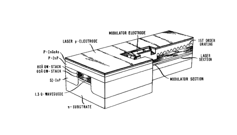
The complete device structure is shown in FIG. ~,. The base
wafer was grown by atmospheric pressure metal organic vapor phase
deposition (MOCVD). The waveguide part was composed of a 250CA thick
1.3 micron InGaAsP layer. Following this layer two stacks of four QW's
30 were grown. The first stack was composed of four InGaAs QW's 60A thick
separated by 100A InC~aAsP barriers. Following this stack a 250A InP
stop-etch layer was grown followed by the second stack of four 80A QW's
separated by 100A InC~aAsP barriers. The last layer grown was a 1.3
wavelength lSOOA thick InGaAsP waveguide layer.
~L:2943~3
- 13-
After the epitaxiai growth, a first order grating coupler was
formed holographically on the top of the last waveguide layer. This
waveguide layer and the top 80A QW stack were then removed at the
modulator section (see FIG. 3) by selective chemical etching down to the
5 InP stop-etch layer.
The rest of the processing steps were similar to those used for
fabricating a semi-insulating blocked planar buried heterostructure (SIPBH)
laser. (See Koren et al., Electronics Letters, Vol. 24, page 138 (1~88)). This
chnique uses two epitaxial regrowth steps by MOCVD for the blocking
emi-insulating layers and for the top cladding and cap layers. Finally, two
electrodes were formed for the laser and modulator parts as shown in FIG.
3. The electrodes were separated by chemically etching through the cap
and most of the cladding layer resulting in about 200 ohms resistance
between the two electrodes.
The devices were cleaved and mounted p-side up on copper
studs. The total cavity length was 500 micron while the central modular
section was 80 micron long. The devices were operated as cleaved without
anti-reflection or high reflectivity coatings on the mirrors.
The change in the effective refractive index of the modulator
20 waveguide as a function of the applied voltage on the modulator electrode is
shown in FIG. 4. The induced phase shift was measured as described in
Koren et al., Applied Physics Letters, Vol. 50, page 368 (1987). The
technique involves driving the laser below threshold so that one can monitor
the spectral shift in the Fabry-Perot modes as a function of the modulator
25 voltage. A phase shift of 1~T corresponds to a shift in the spectrum of one
complete cycle causing it to overlap with the original mode spectrum. Tl1e
excess optical loss that is added to the cavity as the modulator bias voltage
is varied from zero is also shown in FIG. 4. This loss was derived from the
change in contrast of the Fabry-Perot modes. It should be noted that a
30 relatively large change of more than 1~ in the e~fective refractive index was obtained while the excess loss remained smaller than 40 cm-1.
The dominant effect of the modulator voltage on the operation
of the DFB laser is to switch repeatedly (at several different modulator
voltages) between single and double mode operation of the laser. The li~,ht
35 current characteristics for these two states are shown in FIG. 5. The
current threshold for single mode DFB operation is about 10 ma lower than
353
- 14-
for double mode DFB operation, and at single mode operation output power
of above 10 mW/Facet was obta;ned. The spectral behaviou~r below and
above threshold at these two states is shown in FIG. 6. The stop band is
clearly seen below threshold and the laser can be switched between single or
S double mode operation by the modulator voltage. A similar switching
behaviour has been observed previously using variation of the current ratio
in two electrode l~sers. It should be noted that with flne adjustment of the
modulator voltage single mode operation with side mode suppression better
than 40 dB was obtained.
The switching behaviour described above was obtained when the
DFB Bragg wavelength was near to the gain peak of the laser. However,
when the Bragg wavelength was significantly longer than the gain peak
(detuned by 15 nm or more) then we observed switching between DFB
single mode operation and Fabry-Perot operation. Again, switching
lS between these two states occurred several times as the modulator voltage
was varied. This kind of switching behaviour is expected, and indicate that
the threshold for Fabry-Perot operation can be lower, with detuning, than
for double mode DFB operation.
FIG. 7 shows the frequency modulation (FM) response in GHz/V
20 as a function of modulation frequency of the signal applied to the phase
modulator electrode of the intracavity phase modulated DFB laser. This
was measured with a Fabry-Perot interferometer and demonstrates
substantial FM response at GHz modulation speeds.
2. Tunable Quantum Well Bragg Reflectors
In this embodiment a grating, a quantum well and a waveguiding
structure are monolithically fabricated and oriented spatially so that the
forward and reverse versions of a particular optical mode of the waveguiding
structure spatially overlap both the grating and the quantum well. In the
most common embodiments the waveguiding structure will be placed
30 vertically adjacent to the quantum well and the coupler. In the most
common embodiment the grating will be a corrugation in the interface
between two different index materials. The most common application of
this device will be to provide a narrow band reîlection filter whose center
reflection wavelength may be varied by varying the index of the quantum
35 well material, usually by applying an appropriate electric field. This
i 3
- 15-
embodiment is shown schematically in FIG. 8. Provided l~he quantum well
material overlaps the propagating mode in question the effective index of
this mode will be altered when the quantum well material index is altered.
The tuning thus follows directly from 13quation (6). This embodiment may
5 be used as "mirror" in a novel tunable DBR laser, or in a novel tunable
resonant DBR amplif~ler.
3. A Tunable, Reverse ~oupling, (~rating Filter
This embodiment is substantially similar to embodiment number
two above, but rather than coupling between the forward and reverse
I0 versions of a particular optical mode, the grating couples between a forward
version of one particular mode and a backward version of another particular
mode. A specific version of this embodiment will involve a waveguiding
structure which supports two vertically separated spatial modes with
different propagation constants and a grating which will couple both modes
15 usually as a result of its spatially ove~lapping both modes. This
embodiment is shown schematically in FIG. 9. A related prior art device
which does not involve quantum wells is described in "Wave Length
Selective Interlayer Directionally Grating-Coupled InP/InC aAsP Waveguide
Photodetection," Appl. Phys. Lett., 51, 1060 (1~87). In the particular
20 example of this embodiment shown in FIG. ~, a quantum well layer overlaps
at least one of the two spatial modes shown. When the index of the
quantum well layer is varied with an applied voltage, one or both of the
respective mode's effective indices neffl and neff2 may be altered. This has
the effect of changing the coupling wavelength in accordance with Equation
25 (5) which in this embod~ment becomes
g (nef~l + ne~2)
~1. A Tunable, Forward Coupling, Grating Filter
This embodiment, shown schematically in FIG. lO, is
substantially the same as embodiment three above except the two coupled
30 modes are both forward propagating. In accordance with 13quation (7) She
pitch of the grating required for forward coupling is substantially coarser
than that required in reverse coupling. The phase matching wavelength for
this embodiment becomes
3~3
)` = ~B (neSII -- neff2) (9)
5. A Quantum Well Index Modulator Integrated With a Grat;ng
Coupler to Provide a Phase Adjustable Coupling Device
In general, this embodiment involves a grating coupler with a
5 spatially separated quantum well index modulator which may be used to
alter the phase of the coupled light. The phase is altered by providing a
length of propagation in a quantum well medium whose index has been
altered, by application of an electric field, either before or after the coupling
has occurred. The grating coupler itself may or may not also include a
10 quantum well index modulator as in the embodiments one through four
above. Accordingly, FIG. 11 shows five specific examples of this
embodiment. FIG. 11a is a generic schematic diagram of this embodiment
while FIGs. llb through lId are specific examples of this embodiment
analogous to embodiments one through four above.