Note: Descriptions are shown in the official language in which they were submitted.
3~i4
,
~IQUID CRYSTAL DEVICES
The invention relates to smectic liquid crystal devices employing
ferro electric smectic material.
Liquid crystal devices commonly comprise a thin layer o~ a liquid
crystal material contained between two glass ~lates or walls. A
thin transparent electrode is deposited on the inner face of both
walls. ~he combination of liquid crystal layer~ walls, and
electrode is often termed a liquid crystal cell. When an electric
field is applied between the two electrodes, liquid crystal
lo molecule~ rotate in the field to an ON state. On removal of the
field the molecules rotate back to an OFF state, determined by a
surface treatment applied to the wall~ before cell assembly and by
the type o~ liquid crystal material. ~he optical transmission
characteristics of the ON and OFF states are different. Some
devices need one or two polarisers and/or dyes to visibly
distinguish between ON and OFF states.
~here are broadly three different phases of liquid crystal
material, nematic, cholesteric, and smectic, each distinguished by
a different molecular ordering.
Such materials only show a liquid crystal phase over a limited
temperature range between the solid and isotropic liquid phases.
Within the liquid crystal phase temperature range a material may
e~hibit one or more of the nematic, cholesteric or smectic phase
types. Normally a material is chosen such that it forms only one
type of liquid crystal phAse over jts working temperature range.
~'
12~3~3~4
- 2 -
The present invsntion concerns devices using ferro-electric smectic
liquid crystal materials.
Displays have been made with the electrodes formed intc rows on one
wall and cOlUmn8 on the other wall. These collectively form an x,
y matrix of separately addre~sable element~ on a large display.
One way of addre~sing such a display is by multiple~ing i.e.
addressing each row in sequence until the whole display has been
addressed. This is repeated all the time that a display is
0 needed. Another type of display use~ the ON and 0~ states to
form an electrically switchable optical shutter. Yet another type
of di play is used as an optical ~torage device. Nematic
cholesteric and smectic liquid crystal material have been used for
such devices. A problem with many display3 is the time taken to
switch between the two states i.e. the response time~. For many
displays a fa~t response time is needed. A nematic material,
arranged in a 90~ twisted structure typically has a response time
of 100 mJlli~econds.
Devices comprising smectic materials have not been used as widely
a~ device8 With nematic or cholesteric materials. Available
di9play devices based on smectic materials do not have the
necessary characteristics~ Recently however the smectic ferro-
electric property with its fast switching and bistability
characteristics ha~ become important see for example N. A. Clsrk &
S. T. La~erwall, App. Phys. Letters 36(11) 1980 pp 899-901..
Chiral material9 in a tilted liquid crystA1 smectic phase, e.g.
SC . SI SF . SJ, SG* SH*- are known to exhibit ferro-electric
properties. ~hi~ has been described by R. B. Meyer, L. Liebard,
L. Strzelecki, and P. Keller, J. de Physique (Lett.), 36, L-69
(1975)-
12S~-~3
-- 3 --
A disadvantage of the devices using ferro-electric or chiral
smectic (S~) materials is the non-uniformity of cells: they appear
patchy. One particular kind of problem that ari~es in cells u~ing
a conventional alignement layer, such as a rubbed polyimide
material as used in twisted nematic devices, is characterised by a
"zig ~ag" defect, which is visible under microscopic examination
and separates areas of the cell which exhibit different levels of
contrast and angle of view. This produces an unacceptable visual
appearance for a display or shutter using the smectic ~ material.
According to this invention the above problem is solved by using a
cell wall surface treatment that give~ a high tilt to contacting
liquid crystal molecules.
~ 4 ~ 3~4
22762-495
According to this invention a liquid crystal device
comprises:
two cell walls spaced apart by a spacer;
a layer of a chiral (i.e., ferro-electric) smectic
liquid crystal material contained between the walls, the liquid
crystal material having a cholesteric phase at a temperature
above ambient between smectic and isotropic phases;
electrode structures on the inner facing surfaces of
the cell walls;
a surface alignment coating on the inner facing surface
of the cell walls, the alignment coating providing both an
alignment direction and a surface tilt of above 5 to contacting
liquid crystal material;
at least one polariser arranged with its optical axis
parallel to a liquid crystal molecular alignment direction; and
either (i) an amount of a dichroic dye in the liquid
crystal material sufficient to establish a guest-host type
display device or (ii) a second polariser arranged so that the
cell walls are between the polarisers.
The alignment directions on the two walls may be
parallel in the same or opposite directions, although small
variations are acceptable.
A retarder may be incorporated between the polarisers
to optimise colour and contrast.
A reflector may be used and the device viewed in
reflected light, in which case the second polariser may be
replaced by a retarder between the cell and the reflector.
- - 4a - 129~354
22762-495
Preferably, the liquid crystal material has the follow-
ing phases: ~
solid-~ chiral smectic ~_ smectic A~_ cholesteric ~_isotropic.
Preferably, the surface tilt is from about lO to 45C
and the liquid crystal layer is up to 15 ~m thick.
,.i ~ `
1~43~4
The chiral smectic material has a cholesteric phase at a
temperature above ambient between the smectic and isotropic phases.
Preferably the cholesteric pitch p is greatar than half the layer
thickness d over a temperature range of 0.10C or more above the
smectic/cholesteric phase transition. The value of the
spontaneous polarisation co-efficient Ps of the material is at
least 0.1 and preferably 1 or more nC/cm2 .
The liquid crystal material is heated into the isotropic phase and
introduced between the walls by capillary action via two holes
which are subsequently sealed, or by vacumn filling through a
single hole. Once in place the liquid crystal material is heated
into the cholesteric phase and slowly cooled to ambient
temperature. This assists in obtaining good alignment and uniform
appearance. A typical cooling rate is between 0.05 and 2C/minute
within +/- 5C of the smectic/cholesteric phase transition.
Brief Description of the Drawings
One form of the invention will now be described, by way of example
only, with reference to the accompanying drawings in which:-
Figures 1, 2, are plan and section views of a liquid crystal
display device;
Figure 3 is an enlarged view of part of Figure 1;
Figures 4a, b, c are graphs of cholesteric pitch against
temperature for different materials.
Ambient temperatures may be taken as 0C to 40C for most displays.
However for displays mounted on instruments or other equipment
ambient operating temperature may reach 100C.
~ ~43~4
-- 6 --
Description of Preferred Embodiment
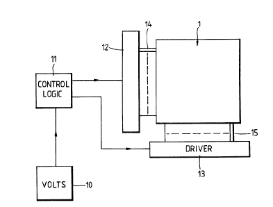
The cell l shown in Figures l, 2, 3 comprises two glass walls 2, 3,
spaced about 2-15 ~m apart by a spacer ring 4 and/or distributed
spacers. Electrode structures 5, 6 of transparent tin oxide are
formed on the inner face of both walls. These electrodes may be
of conventional row (x) and column (y) shape, radius and angle (r,
~) shape, or seven or more segment display for displaying alpha
numerics. A layer 7 of smectic liquid crystal material is
contained between the walls 2, 3 and spacer ring 4. Polarisers 8,
9 are arranged in front of and behind the cell 1. A d.c. voltage
source 10 supplies power through control logic 11 to driver
circuits 12, 13 connected to the electrode structures 5, 6, by lead
wires 14, 15.
The cell display may be observed by transmitted light, in which
case a light source eg a tungsten bulb 16 is arranged behind the
display. Alternatively a reflector 17 may be arranged behind the
polari~ers and the display observed by reflected light.
Additionally a retarder (not shown) may be arranged between wall 3
and polariser 9.
Prior to a~sembly the walls 2, 3 coated with the electrodes 5, 6
are surface treated by the known process of oblique evaporation of
silicon monoxide.
354
-- 7 --
This is described for example in G.B. 1,454,296, 1,472,247,
l,470,592. A ~tream of silicon monoxide i~ deposited onto a wall
at an angle of up to 15~to the substrate surface. When used as
described in the above qpecification with nematic liquid crystal
S materials this results in a uniform linear alignment of liquid
crystal molecules and a tilt of 30 D between the molecules and the
wall. The alignment is analogous to rubbing which provides
alignment of liquid crystal molecules but a tilt of about 2.
Different angles of molecular tilt may be produced by sequential
evaporation of SiO at evaporation angles Df up 15. and angles
between 15and 30~. Varying the amounts of material deposited in
these two directions Varies the tilt angle between about 0 and
45 -
The smectic material is preferably one having a long pitchcholesteria phase above the smectic phase.
To provide a uniform alignment of both molecules 26 and micro-
layers 25 it is nece~sary to use a smectic material with a
cholesteric phase at elevated temperatures flbove device operating
temperatures e.g~ above 40C or eVen 100C depending on device use.
~igure 4a shows a cholesteric pitch p versus temperature curve for
a typical conventional smeCtiC material With a cholesteric phase.
As the temperature reduces very clo~e to a cholesteric/smectic
phase transition, pitch p increases towards infinity. Away from
this transition cholesteric pitch becomes very small, typically
much less than 1 ~m.
-- 7 --
12~354
Display8 of the invention described in copending application
numbers GB 86 08,114 and 86 08,115 filed together with the present
invention have a long pitch in the cholesteric phase fcr at least
0.1C above thi 8 phase transition. Preferably this range is 5OC
and ideally occurs over the whole cholesteric temperature range.
Within this range the minimum p is greater than 4d, d being the
layer thickness.
There are a number of ways of achieving the above material. ~or
example combining one or more chiral components with laevo (left)
cholesteric twist sense with one or more chiral components with
dextro (right) cholesteric twist sense, with the proviso that none
of the laevo components are the racemates of the dextro components.
Such a mixture may be used by itself if it has the necessary
smectic phases. Alternatively the chiral mixture may be added to
a non-chiral or a racemate liquid crystal material, e~ a smectic C
host. Different chiral components may have different
temperature/pitch characteristics. In this case it is necessary
to ensure that the re8ultant pitCh ha8 the required value in the
temperature range above the smectic/cholesteric phase transition.
When using chiral components of opposite twist sense it is
necessary to ensure that the resultant mixture has the required
spontaneous polarization value Ps. Thus all of the chiral
components, regardless of their cholesteric twist sense, may have
the same sense of S * polarization, i.e. their Ps add.
Alternatively one or more of the chiral components may have the
opposite sense of Ps providing the net Ps has a sufficient value.
lZg43~4
- 9 -
Another way of achieving the above material i9 to u3e one or more
chiral components with the same cholesteric twist sense and S *
polarisation sense but still satisfying the cholesteric pitch
values noted above. Such a mixture may be used alo~e or in
combination with a non chiral or a racemate liquid cryRtal
material, eg a S C host.
As a result of the long pitch in the cholesteric pha~e the material
cools into the Sc* pha~e with uniform alignment caused by the cell
wall treatment. The result i~ alignment as in ~igure 3.
The pitch in the smectic phase is arranged to be greater than about
l ~um and preferably very much greater.
The compensation of pitch in the cholesteric phase is illustrated
in Figures 4(a), (b), (c). Figure 4(a) shows cholesteric pitch
against temperature for a noncompensated material having a
cholesteric to smectic transition. At this transition the pitch
tends to infinity. The compensated material shown in Figure 4(b)
shows a pitch increa3e a few degrees above the transition
temperature with a pitch reduction below. By suitable selection
of materials thi~ pitch increase can be made to occur even closer
to the transition temperature as in ~igure 4(c) , but a few degrees
difference does not seem to affect the end result.
_ g _
a3~4
1 o --
When introduced into a cell liquid crystal molecules at the cell
walls align along the evaporation direction of SiO marked E on
Figure 3 with a surface tilt of eg 30. The directi~ns of E may be
the same or in opposite directions on the two walls 2,3. Liquid
crystal molecules are observed to adopt one of two ali~nment
direction Dl~ D2 depending on the polarity of an applied voltage.
A typical voltage is +/- 10 to 50 volts. These two positions are
seen in Figure ~ in full Dl and broken lines D2~ and lie either
side of the evaporation/alignment direction E. Rapid switching
between the two states, when the d.c. pulses are applied, is due to
the smectic ferro electric property of the material. ~ypically
the cell can be switched between D1 and D2 in times of a few ,us to
a few ms eg 1ms depending on the liquid crystal material. The two
different directions D1, D2 represent two different directions of
Ps, often termed UP and DOWN directions. These two directions D1,
D2 may be about 45 apart depending on the material composition.
-- 10 --
12~3~4
The polarisers ~, 9, Figures 1, 2, are arranged with their optical
axes crossed. Polariser 8 is aligned with it~ axis parallel to
direction Dl. The cell 1 transmits light polari3ed in a plane
parallel to the direction of molecular alignment D1 or D2. ~hus
in one state D1 of the cell very little light is passed through the
combination of polariser 8, cell 1, and polariser 9.
However when the cell is in state D2 the molecules are at 45 to
both polarisers 8, 9 optical axis and light is transmitted.
Typical applied voltages are +/- 15 to 20 volts for a 6 jum thick
layer of liquid crystal material, +/- 5 to 10 volts for a 2~um
thick layer, and +/- about 30 volts for a 12 ~um thick layer.
For the x, y matrix display of Figure 1 each electrode intersection
x, y is addressed by a +/- voltage pulse; m, n are integers equal
to the number of 2 and y electrodes respectively. These pulses
switch the liquid crystal material at each xm, yn intersection to
be light trRnsmissive or opaque as required. Using a kno~m
technique of multiplex addressing each intersection is addresAed in
sequence. Such addressing may be an interseetion at a time or a
whole x row at a time.
Conventionally an x, y matrix needs to be continually refreshed,
i.e. re-addressed, to maintain a flicker free display. The reason
for thi9 i9 that conventional nematic materials quite rapidly relax
from one say ON state to say an OFF state. Conventional
addressinB refreshes each intersection before they have time to
turn from ON to OFF. This imposes a severe limitation on the
number of x, y intersections that can be addressed.
354
In contrast cells of this invention possess true bistability.
That is when switched into either D1 or D2 state they remain as
switched for some seconds or even hours, depending on the cell
material and construction, without any applied voltage until
switched to the other state. This means that much larger numbers
of intersections can be addressed without flicker of the display.
Alternatively instead of refreshing the whole display only those
parts to be changed are addressed.
Materials suitable for use in cells of this invention are:-
Example 1
CM6 =43.5% CD3 (chiral component) + 56.5% H1 (S host)15
where CD3 = 22% CC1 + 78% CC3
Me
CC1 = C ~ l7 ~ COOC*HC6H13
Me
CC:5 C8H17~COO~ ~ *
F
25 Hl = Ml + M2 + M3 (1:1:1 )
Ml = C8H17 {~}COO~c5
F
M2 = C8H170~Coo~c5Hll
M3 = C7Hl50 ~ C00 ~ C7Hl5
F
- 12 -
3~4
CM6 h~ the follownn~ ph~e~
solid ~ chiral ~mectic = ~mectic A ~ cholecteric`~- isotropic
Example 2
Merck ZLI 3041
Example 3
LPMl3:- 72.5% Hl + 25% M7 + 2.5g CC13
lS ~7 = C8H17 ~ COO ~ C5H11
CN Me
CC13 C8H17 ~ C02C*H C H
Me
LLM13 has the following phases:-
solid,chiral smectic 56.3 cholesteric 118 isotropic.
Ps = lOnC/cm at 20C and 5nC/cm2 at 460C.
One example of a blue dye is Dl02 available from BDH Poole, Dorset,
UK.