Note: Descriptions are shown in the official language in which they were submitted.
.;375
SELF REGULATING TEMPERATUR~ HEATER AS AN
INTEGRAL PART OF A PRINTED CIRCUIT BOARD
The present invention relates to an improved method
and apparatus for electrically connecting and
disconnecting contaCt pads or traCes on a circuit board to
and from external leads. More particularly, the present
invention relates to improvements in positioning and
utilizing self-regulating heaters to effect electrical
connections and disconnections at circuit pads on a
circuit board.
Although the invention has as its primary utility the
simultaneous joining of a plurality of electrical leads to
a plurality of circuit board contacts, it will be
appreciated that the principles described herein are
equally applicable to joining a single lead to a single
contact. Moreover, although the description set forth
below mentions solder as the joining material, it is to be
understood that any fusible material, such as doped
conductive plastic material, may be employed.
Soldering cable leads to circuit board contact pads
can be achieved in a variety of prior art methods and
apparatus. The least desirable of these is manually
effecting each of the multiple solder terminations; that
is, the resulting repetitive soldering operations are
time-consuming and costly. In addition, close spacing
between adjacent connection sites renders it likely that
14325 CA
375
SELF REGULATING TEM~ERATURE HEATER AS AN
INTEGRAL PART OF A PRINTED CIRCUIT BOARD
The present invention relates to an improved method
and apparatus for electrically connecting and
disconnecting contact pads or traces on a circuit board to
and from external leads. More particularly, the present
invention relates to improvements in positioning and
utilizing self-regulating heaters to effect electrical
connections and disconnections at circuit pads on a
circuit board.
Although the invention has as its primary utility the
simultaneous joining of a plurality of electrical leads to
a plurality of circuit board contacts, it will be
appreciated that the principles described herein are
equally applicable to joining a single lead to a single
contact. Moreover, although the description set forth
below mentions solder as the joining material, it is to be
understood that any fusible material, such as doped
conductive plastic material, may be employed.
Soldering cable leads to circuit board contact pads
can be achieved in a variety of prior art methods and
apparatus. The least desirable of these is manually
effecting each of the multiple solder terminations; that
is, the resulting repetitive soldering operations are
time-consuming and cost~y. In addition, close spacing
between adjacent connection sites renders it likely that
14325 CA
*
43~i
Another prior art problem associated with the
simultaneous soldering of sets of plural contacts relates
to solder bridging between the connection sites. The
pressure and thermal energy applied to spaces between the
connection sites tends to cause the solder to run between
those sites and form solder bridges. This problem has
been addressed in some prior art apparatus such as that
disclosed in the aforementioned Grassauer et al patent.
In that apparatus the solder is sandwiched between two
layers of polymeric material, one of Which has window
openings arranged to permit the solder, when melted, to
flow through to respective connection sites. Barriers are
provided between the windows to preclude solder bridging.
While this technique, when properly employed, minimizes
bridging, proper employment iS hampered by the difficulty
of aligning the windows (which must necessarily face
downward and away from the technician) with respective
contact pads at the connection sites. Care must also be
taken to avoid displacement of the solder within the
layered polymeric package prior to heating the apparatus
in order to assure that solder is present at each of the
window openings.
Connectors having terminals with solder tails
extending therefrom for reception in plated through holes
of a circuit board are well known. Relatively recently,
in the interests of facilitating automated contact
14325 CA --3--
~Z943 ~S
placement and economy of circuit board manufacture,
surface mount connectors have been developed with
terminals having solder tails formed for disposition
against respective plated contact pads on the surface of
the board. The terminals are typically fixed in the
connector housing, and the tails are formed to sufficient
length to assure compliance with the pad or pads,
regardless of any tendency of the board to warp.
Typically, each solder tail is individually manually
soldered to a respective contact pad by any of a variety
of known techniques. The repetitive soldering operations
are both time-consuming and costly.
Another problem associated with prior art techniques
for simultaneously joining multiple solder tails of a
surface mount connector to respective contact pads on a
printed circuit board relates to positionally aligning of
the components during soldering. It is not only necessary
for the multiple solder tails to be positionally aligned
with respective multiple contact pads on the printed
circuit board surface; in addition, the solder tails and
contact pads must be simultaneously aligned with multiple
respective sections of the solder delivery unit. The
resulting alignment procedure is often unwieldy at best.
It is desirable, therefore, to provide a method and
apparatus for electrically joining contact pads of a
circuit board to respective leads in a cable or solder
14325 CA -4-
~Z~37~
67789-271
tails of a surface mount connector without a third component to be
aligned at each connection site. In addition, it is desirable
that the thermal energy required to melt the fusible material
(e.g. solder) be available virtually instantaneously after
energization of the heater, and tha~ the heater be arranged to
provide no more thermal energy than is required to melt the solder
at the varioUs connection sites. It is also desirahle that the
heater be simple and convenient to employ and energiz~, and that
it have a relatively low mass in order that the heater may cool
quickly after a soldering operation. It is likewise desirable
that the method and apparatus provide the thermal energy to a
locallzed area in which the connection sites are located.
The present invention makes use of a relatively new
automatic self-regulatiny heater technology disclosed in U.S.
Patent Nos. 4,256,g45 (Carter et al), 4,623,401 (Derbyshire et
al), 4,659,912 (Derbyshire), 4,695,713 (Krumme), 4,701,587 (Carter
et al), 4,717,814 (Krumme) and 4,745,264 (Carter). A heater
constructed in accordance with that technology, referred to herein
as a self-regulating heater, employs a substrate of copper, copper
alloy, or other material of low electrical resistivity, negligible
magnetic permeability and high
7~
thermal conductivity. ~ thin layer of
thermally-conductive magnetic material is deposited on all
or part of one surface of the substrate, the layer
material typically being an iron, nickel or nickel-iron
alloy, or the like, having a much higher electrical
resistance and magnetic permeability than the substrate
material. The thickness of the layer is approximately one
skin depth, based on the frequency of the energizing
current and the permeability and resistance of the layer.
A constant amplitude, high frequency alternating
energizing current is passed through the heater and, as a
result of the skin effect phenomenon, is initially
concentrated in one skin depth corresponding to the
thickness of the magnetic surface layer material. When
the temperature at any point along the heater reaches the
Curie temperature of the magnetic material, the magnetic
permeability of the magnetic material at that point
decreases dramatically, thereby significantly increasing
the skin depth so that the current density profile expands
into the non-magnetic substrate of low resistivity. l'he
overall result is a lower resistance and lesser heat
dissipation. If thermal sinks or loads are placed in
contact with the heater at different locations along the
heater length, thermal energy is transferred to the loads
at those locations with the result that the temperature
does not rise to the alloy Curie temperature as quickly at
14325 CA -6-
12~3~ii
67789-271
those locations as it does in the non-load locations. ~he
constant ampli~ude current remains concentrated in ~he higher
resistance alloy layer at the load locations which dissipate
considerably more resistive heating energy than it dissipated in
the non-load locations where the current is distributed in the low
resistance substrate.
It is therefore desirable to provide a technique for
connecting and disconnecting circuit board contact pads to
external leads and terminals whereby a self-regulating heater may
be employed for both connecting (i.e., soldering) and
disconnecting (i.e., unsoldering) applications. Moreover, it is
desirable to provide a method and apparatus for effectlng
electrical connections and disconnections at circuit board contact
pads wherein a heater for generating thermal energy to melt solder
or other fusible material is a permanent part of the circuit board
structuxe.
In accordance with the apparatus of the present
invention, there is provided an artlcle containing portions to be
heated by delivery of sufiicient thermal energy to at least one
connection site to melt electrically-conductive fusible material
at the connection slte, said article comprlsing: a support
structure comprising an electrically-insulative thermally-
conductive circuit board havlng first and second opposite b~ard
surfaces spaced by a board ~hickness dimension, with at least one
contact pad secured to said circuit board at said connection site,
n~
1294375
677~9-271
said pad being disposed on said first board surface; a selectively
energizable self-regulating heater ~or generating said sufficient
thermal energy, said heater having a thermally-conductive portion
permanently secured to said support structure in spaced proximity
to said connection site to permit thermal energy generated by said
heater to be conducted to said connection site through the circuit
board, said heater having a substrate of electri~ally and
thermally conductive non-magnetiC substrate material having first
and second opposite surfaces, the suhstrate disposed over less
than the entirety of said second surface o~ said circuit board and
secured to said circuit board with the second substrate surface
against the second board surface, a surface layer of at least a
part of said first substrate surface, said surface layer aligned
with said pad through the thickness of said circult board, said
surface layer material being electrically and thermally conductive
but having a much greater electrical resistance than said
substrate material, whereln said self-regulatlng heater is
energizable by passing a constant amplitude alternating current of
known frequency therethrough and the depth of said surface layer
20 on said first surface of said substrate iS approximately one skin
depth at said known frequency, whereby current through said heater
is concentrated in said surface layer at temperatures below the
Curie temperature of said surface layer material and expands into
said 5ubstrate material at temperatures equal to and above said
Curie temperature.
4375
67789-271
The invention will now be described by way of example
with reference ta the accompanying drawings, in which
FIGURE 1 is a View in perSpective of one embodiment o~
the present invention whereln a circuit board has a self-
regulating heater mounted on one surface thereof;
. FIGURE 2 is a sectional view in elevation taken along
lines 2-2 of Figure 1 and showing a surface mount connector
positioned to be soldered to contact the circuit board;
FIGURE 3 is a sectional view in elevation similar to
Figure 2 but of a modified version of the embodiment of Figure 1,
FIGUR~ 4 is an exploded vlew in perspective of another
embodiment of the present invention in which a
~2~375
multi-layer circuit board has a plurality of
self-regulating heaters embedded therein;
FIGURE 5 is an sectional view in elevation taken
along lines 5 - 5 of Figure 4;
FIGURE 6 is an sectional view in elevation taken
along lines 6 - 6 of Figure 4:
FIGURE 7 is an sectional view in elevation of another
embodiment of the present invention wherein a
self-regulating heater is embedded in a circuit board and
lo illustrating a surface mount connector positioned to be
soldered to circuit board contact pads;
FIGURE 8 is a sectional view in elevation of another
embodiment of the present invention wherein a
self-regulating heater is embedded in a circuit board to
which a flexible etched cable is positioned to be soldered
to circuit board contact pads; and
FIGURE g is a sectional view in elevation of still
another embodiment of the present invention wherein a
self-regulating heater is embedded in a circuit board and
a multi-conductor cable is positioned to be soldered to
contact pads on a surface of the circuit board.
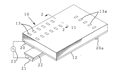
Referring specifically to Figures 1 and 2 of the
accompanying drawings, a circuit board 10 has a top
surface 11 and a bottom surface entirely covered by a
substrate 12. Substrate 12 is composed of copper, copper
alloy or other material having a high electrical
14325 CA -10-
~ 37 5
conductivity (i.e., low resistivity) and negligible
magnetic permeability (i.e., a permeability at, or close
to, one). The substrate material must also be a good
thermal conductor. In this embodiment, wherein substrate
12 covers the entire bottom surface of the circuit board,
the length and width of the substrate are determined by
the corresponding board dimensions. The depth of the
substrate may be dictated by circuit board structural
requirements; however, for purposes of heater function,
o the depth of the substrate need only be on the order of a
few thousands of an inch.
~ plurality of contact pads or traces 13 are disposed
in a conventional manner on the top surface ll of circuit
board 10. Traces 13 are arranged in two mutually spaced
longitudinal rows wherein the traces are positioned to
correspond to the positions of two rows of solder tails 14
of a surface mount connector 15. Another set of traces
13a is positioned at another portion of top surface ll Of
the circuit board and arranged in a row so as to be
connected, for example, to wires or leads of a cable.
In order to form a self-regulating heater, a
thermally-conductive surface layer 20 of magnetic material
is deposited or otherwi5e affixed to a portion Of the
exposed surface of substrate 12 located in registration
with the two rows of contaCt pads 13 at top surface 11. A
similar surface layer 20a is affixed to the same surface
14325 CA -11-
L37~i
of substra~e 12 but in registration with the row of
contact pads 13a to define a second self-regulating
heater. The two self-regulating heaters may be
individually or simultaneously energized, as desired. The
~ollowing description of the characteristics of surface
layer 20 is intended to apply to surface layer 20a.
A typical material for surface layer 20 is
nickel-iron alloy, such as Alloy 42 (forty-two percent
nickel, fifty-eight percent iron) or Alloy 42-6 (forty-two
percent nickel, six percent chromium, fifty-two percent
iron); however, layer 13 may be any metal or alloy having
the characteristics described herein. Depending upon the
particular material, magnetic permeabilities for surface
layer 20 range from fifty to more than one thousand, as
compared to a permeability of one for copper; typical
electrical resistivities range from twenty to ninety
micro-ohms per centimeter as compared to 1.72 for copper.
The thickness of surface layer 20 is typically one skin
depth. In this regard, substrate 12 and surface layer 20,
when energized by passing a constant amplitude alternating
current therethrough, function as a self-regulating
heater. Specifically, for temperatures below the Curie
temperature of the surface layer material, slightly more
than sixty-three percent of the constant amplitude current
flowing through the heater is concentrated in one skin
depth from the heater surface. The s~in depth is
14325 CA -12-
3~75
proportional to the square root of the material
resistivity, and is inversely proportional to the square
root of the product of the magnetic permeability of
surface layer 20 and the frequency of the alternating
5 current passing through the heater. For temperatures
equal to or above the Curie temperature of the surface
layer, the magnetic permeability of the material drops to
approximately that of the substrate material (i.e., a
permeability of one, for copper), thereby producing a
dramatic increase in the skin depth. Consequently, much
more of the constant amplitude current is distributed in
the lower resistivity substrate 12 than in the higher
resistivity surface layer 20, with the result that
considerably less heat is dissipated. If selected
locations of the heater body are in contact with thermal
energy absorptive loads (e.g., heat sinks~, then the
temperature at those locations of the heater body does not
rise as readily as it does at the non-load locations. It
is possible, therefore, for the constant amplitude current
to be concentrated in layer 13 to a greater extent at the
load locations (where the temperature is below the curie
temperature for surface layer 20) than at the non-load
locations (where the temperature is equal to the Curie
temperature of the surface layer material). Curie
temperatures for materials can range from 50c to 1,ooO~C;
typical materials employed for surface layer 20 have Curie
14325 CA -13-
12~375
temperatures in the range of 200C to 500C, depending
upon the solder or other fusing material employed.
In order to actuate the heater associated with
surface layer 20, a tooling assembly is employed and
comprises a conductive bus bar layer 21 and a superposed
layer 22 of electrically insulative material. The bus bar
layer 21 is typically copper and has dimensions similar to
those of surface layer 20. Insulative layer 22 is
typically Kapton and is slightly larger in length and
width than the corresponding surface layer dimensions; the
thickness of layer 22 is of the same order of magnitude as
that of the substrate. When it is desired to energize the
heater, the tooling assembly is positioned flush against
the heater with the exposed surface of insulative layer 22
abutting surface layer 20 of the heater. The heater and
tooling assembly may be held together by clamps or other
suitable means while the heater is energized.
As best illustrated in Figure 1, a source 23 of
constant amplitude alternating current is connected across
the heater (at substrate 12) and the tooling assembly (at
bus bar 21) at one longitudinal end of the heater. Source
23 may be any suitable constant amplitude alternating
current supply such as, for example, the source disclosed
in U.S. Patent No. 4,626,767 (Clappier et al) and provides
25 a constant amplitude alternating signal, typically in the
radio frequency range. Most commonly, the frequency of
14325 CA -14-
12~43 ~5
the actuating signal is 13.56 MHz. The constant amplitude
of the signal is selected to provide the desired heating
level. An impedance matching circuit is generally
provided to match the impedance of the heater-tooling
combination to the source impedance.
At the end of the heater section located
longitudinally remote from the connection to source 23,
there is a short circuit connection 24 (Figure 2)
interconnecting substrate 12 and bus bar 21. For example,
the short circUit 24 may be a copper strap positioned on
the tooling to electrically connect the substrate to the
bus bar when the tooling assembly is placed adjacent the
heater. Current flow at any instant of time is in
longitudinally opposite directions in substrate 12 and bus
bar 25. A resulting electric field is established between
the substrate and the bus bar across the insulation layer
22, thereby concentrating the current flowing through the
heater in the high reslstance surface layer 20 rather than
in the lower resistance substrate. The current flowing
through bus bar 21 is similarly concentrated at the
surface facing the surface layer 20. Since the current
amplitude is maintained constant, it is desirable, for
optimal heating, to concentrate the current in the higher
resistance layer 20 of the heater than in the lower
resistance substrate 12. That is, the resistive heating,
with the current maintained constant, is greater when the
14325 CA -15-
1294375
current path has greater resis~ance. The electric field
developed by the oppositely-directed current flowing in
the heater and bus bar assures that the current in the
heater is concentrated in the high resistance surface
layer of the heater assembly facing the bus bar.
Thermal energy generated by resistance heating in
surface layer 20 is conducted via the substrate 12 and the
structure material of circuit board 10 to the contact pads
13 at the top surface of the circuit board. The nature of
the self-regulating heater is such that the resistance
heating is produced only where it is needed to effect
soldering operations. More specifically, current through
the heater flows longitudinally (i.e., into and out of the
plane of the drawing in Figure 2) and thereby encounters
regions relatively proximate contact pads 13 and regions
relatively remote from the contact pads. Thermal energy
developed in regions proximate the contact pads is
conducted to respective connection sites by the structure
material of circuit board lO, thereby preventing the
temperature at those regions from building up quickly.
On the other hand, in the regions relatively remote from
the contact pads, the temperature increases rapidly until
it reaches the Curie temperature of the surface layer
material, whereupon the effective skin depth is increased
in those regions. This causes more current to flow
through the low resistance substrate material in these
14325 CA -16-
34375
regions and, as a consequence, less thermal energy is
produced therein. The regions located proximate the
contact pads continue to develop high amounts of thermal
energy that is transmitted to the respective connection
sites through the circuit board structure material.
Overheating of the connection sites is prevented by the
same mechanism; that is, once the temperature at a
connection site reaches a certain level, thermal
conduction from the heater to the site ceases, thereby
removing the heat sink effect of the connection site. The
thermal energy developed by current flowing in the high
resistance surface layer 20 then quickly increases the
temperature at heater locations proximate the connection
site until the Curie temperature of the surface layer
material is reached. Eventually the effective skin depth
along the entire length of the heater is increased so that
more of the constant amplitude current flows through the
low resistance substrate 12 and significantly less thermal
energy is produced by resistive heating. After current is
removed from the heater assembly, the assembly begins to
cool and the solder, or other fusible material, at the
connection sites is permitted to harden~ The cooling
proceeds quickly because the relatively low mass of the
heater does not retain its heat for long periods of time.
The tooling assembly, including the return bus 21,
insulation layer 22, source 23 and short circuit 24, may
14325 CA -17-
37~
be removed from the heater at any time after current flow
is terminated.
The self-regulating heater composed of substrate 12
and surface layer section 20a may operate with the same or
different tooling components used for the heater composed
of substrate 12 and surface layer section 20, In either
case, operation is the same as described above for the
heater comprised of substrate 12 and heater section 20.
The self-regulating heater assembly need not have a
lo substrate that covers the entire bottom surface of the
circuit board. For example, a substrate may be disposed
only on those areas of the underside of the board that are
in registration with the connection sites. An example of
an embodiment of this type is illustrated in Figure 3
wherein substrate 17 is disposed in registration with
contact pads 13. SUr~ace layer 20 is disposed over the
entire exposed surface of the substrate. In all other
respects the embodiment illustrated in Figure 3 is the
same as the embodiment illustrated in Figures 1 and 2 and
operates in the same manner. It will be appreciated that
substrate 17 and its surface layer 20 can be configured to
extend into registration with contact pads 13a tFigure 1)
and any other connection sites on the circuit board so
that a single heater can be energized to simultaneously
effect soldering at all connection sites on the board.
Likewise, when a substrate 12 (Figures 1 and 2) co~prising
14325 CA -18-
375
the entire underside of the board is employed, a single
surface layer 20 may be configured to register with all
contact sites to be simultaneously heated.
Circuit board 10 is composed of any material
conventionally employed for circuit board structures. The
material must provide the necessary structural support and
must be electrically non-conductive. In addition, the
structure material must transmit thermal energy from the
heater to the connection sites over at least the short
o distances required by the present invention. Examples of
suitable materials are ceramic, glass, glass epoxy and
various phenolic materials.
In accordance with the present invention, a
self-regulating heater may also be embedded in a
multi-layer circuit board and selectively energized to
generate thermal energy for melting solder or other
fusible material at one or more connection sites on the
board. With references to Figures 4, 5 and 6 of the
accompanying drawings, a multi-layer circuit board
assembly 30 includes a top layer 31, an intermediate layer
32 and a bottom layer 33 sandwiched together in a stack.
Adjacent layers are secured to one another in a
conventional manner, such as by adhesive, ultrasonic
welding, screws, etc., and the material used for the
individual layers is the same as the structure material
described above as used for circuit board 10 in Figure 1.
14325 CA -19-
37~
With particular reference to Figures 4 and 5, a plurality
of contact pads or traces 34 are spaced in a
longitudinally-extending row at the top surface of upper
board layer 31. The top surface of intermediate board
layer 32 has a recess defined therein in an area aligned
in depthwise registration with the row of contact pads on
upper board layer 31. Disposed and secured in that recess
is a self-regulating heater 40 including a substrate 41
and surface layer 42 having the same thermal, electrical
and magnetic properties as substrate 12 and surface layer
20, respectively, of Figure 1. The length and width
dimension of heater 40 are the same as those of the recess
in which it resides and are determined by the area
encompassed by the row of contact pads 34. The underside
of intermediate board layer 32 is also provided with a
recess in Which a return bUs 43 of conductive material
(e.g., copper) is disposed. The return bus 43 and its
retaining recess are aligned depthwise with heater 40 and
its retaining recess. Heater 40 is oriented such that
surface layer 42 is parallel to and closely spaced from
return bus 43 across the intervening structure material of
intermediate board layer 32. The opposite surface of
heater 40 (i.e., the top surface of substrate 41) is flush
with the top surface of inte~ediate board layer 32 and
abuts the underside of top board layer 31. Substrate 41
is typically a few thousands of an inch thick. The
14325 CA -20-
3~
thickness of the surface la~er 42 is approximately one
skin depth of the surface layer material at the frequency
of the energizing signal for the heater. Return bus 43 is
disposed in its recess such that the bottom surface of the
return bus is flush with the bottom surface of
intermediate board layer 32 and abuts the top surface of
bottom board layer 33.
At one end of the row of contact pads 34 there are
two terminals 35, 36 affixed to the top surface of the top
board layer 31. Terminals 35, 36 are adapted to be
connected to respective opposite sides of a source 23 of
constant amplitude alternating energizing current.
Terminals 35, 36 are connected to the heater 40 and return
bus 43, respectively, at one end of the heater by any
conventional electrically-conductive means extending
depthwise into the structure. For example, terminal 35 is
illustrated as comprising the upper end of a conductive
post or pin 37 extending through the entire thickness o~
upper board layer 31 into ContaCt With a Con~act trace 44
or similar conductive strip disposed at the top surface of
intermediate board layer 32 and extending into direct
electrically-conductive contact with one end of heater
substrate 41. Terminal 36 is illustrated as comprising
the upper end of a conductive post or pin 38 extending
through the entire thickness of upper board layer 31 and
intermediate board layer 32 into contact with a contact
14325 CA --21--
lZ~3~7~
trace 45 or similar conductive strip disposed at the
bottom sur~ace of intermediate board layer 32 and
extending into direct electrically-conductive contact with
the same end of return bus 43. The opposite ends of the
heater and return bus are electrically connected together
by any suitable means such as a pin or post 46 extending
through the thickness of intermediate board layer 32 into
contact with respective traces 47, 48, or the like,
extending from the heater 40 and return bus 43 at
respective surfaces of the intermediate board layer.
When source 23 is connected across terminals 35, 36,
the resulting current is, at any instant of time,
oppositely directed through heater 40 and return bus 43.
As a consequence of the oppositely directed currents, an
electric field is established across the heater and return
bus, the field serving to concentrate heater current at
the surface facing the return bus ti.e., the surface clad
with surface layer 42). Thermal energy is generated in
the manner described above in relation to Figures 1 and 2
and is transmitted to the connection sites at contact pads
34 from substrate 41 through the intervening structure
material of upper board layer 31.
It is possible to provide thermal energy for melting
solder at contact pads 60 constituting conn~ction sites
25 located on the underside of bottom board layer 33.
Referring to Figures 4 and 6, a second self-regulating
14325 CA -22-
37~
heater 50 is aligne~ depthwise with the area encompassed
by contact pads 60 and disposecl in an appropriately
defined recess in the bottom s~lrface of inter~ediate board
layer 32. Heater 50 includes a substrate 51 with its
magnetic surface layer 52 facing away from contact pads
60. A return bus 53 is disposed in a suitable recess in
the top surface of intermediate board layer 32 in
depthwise alignment with heater 50. Terminals 54, 55,
disposed at the top surface of upper board layer 31, are
adapted to be connected to opposite sides of energizing
current source 23. Terminal 54 is electrically connected
to one end of heater 50 by a conductive post or pin 56
extending depthwise through the entire thickness of board
layers 31 and 32 into contact with a circuit trace 57, or
the like, at the bottom surface of intermediate board
layer 32. Trace 57 is in direct electrical contact with
substrate 51. A similar post or pin 58 extends from
terminal 55 through the thickness of upper board layer 31
into contact with circuit trace 59 at the top surface of
intermediate board layer 32. Trace 59 is in electrical
contact with one end of return bus 53 corresponding to the
aforesaid one end of heater 50. The opposite ends of
heater 50 and bus 53 are connected together, such as by a
connective strip 61. Heater 50 functions in the manner
described above in relation to heater 40.
14325 CA -23-
12~375
In the embodiment illustrated in Figure 7, a heater
70 comprising substrate 71 and magnetic surface layer 72
is embedded in the circuit board 75. Contact pads 13,
disposed on the top surface of the board, are positioned
to be soldered to respective solder tails 14 of surface
mount connector 15. Instead of embedding the return bus
in circuit board 75, return bus 73 is secured to, or
substantially movable into flush abutting contact with,
the unde~side of the board. The magnetic surface layer 72
of the heater faces the return bus 73 in parallel
closely-spaced relation across the structure material of
circuit board 75. Embedded heater 70 functions with
external return bus 73 in the same manner described above
for the embedded heaters illustrated in Figures 4, 5 and
6. An exposed terminal (not shown) on the circuit board
permits one side of an energizing source to be connected
to heater 70, the other side being connected to return bus
75. A connection (also not shown) between the heater 70
and return bus 73 may be entirely embedded in the board,
or may include an exposed terminal at a board surface to
which an external wire, or the like, may be connected for
shorting the heater to the return bus.
Figure 8 is an illustration of an embodiment in which
conductors in a flexible etched cable 84 are soldered or
otherwise fused to respective contact pads 83 on a circuit
board 86. The embedded heater 80 includes a substrat.e 81
14325 CA -24-
12~ 375
with its magnetic surface layer 82 aligned with contact
pads 83 in spaced relation. Surface layer 82 faces the
contact pads and is separated therefrom by the
electrically-insulative structure material of board 86.
To effect soldering, the conductors of cable 84 are
disposed on respective contact pads 83, and an external
return bus 85 is disposed on the cable so that the
connection site, including the contact pad and cable
conductor, is disposed between the heater 80 and the
return bus. A constant amplitude alternating current
energizing source (not shown) is connected between
corresponding ends of the heater and return bus,
respectively, as described above. Likewise, a short
circuit (not shown) is connected between the opposite ends
of the heater and return bus. Operation proceeds in the
manner described above to provide the energy required to
melt the solder or other fusible material at the
connection sites.
The embodiment illustrated in Figure 9 is identical
to that illustrated in Figure 8 except that an individual
lead or conductor 94 is shown being soldered to contact
pad 83 rather than the flexible etched cable 84 of Figure
8. Conductor 94 is provided with an insulation sleeve 95
throughout most of its length, the slee~e being stripped
at one end of the lead to permit the required electrical
14325 CA -25-
lZ~375
contact at the connection site. Lead 94 may ~e part of a
multi-conductor cable or it may be a single lead.
In the embodiments described above in which the
heater is embedded in the circuit board, it is to be
understood that the heater body may be inserted into
pre-formed recesses at a board surface; alternatively, the
substrate and magnetic surface layer Of the heater may be
formed by deposition, or similar technique, during the
fabrication of the board structure. In other words, any
technique for embedding the heater in the board material
is considered to fall within the scope of the present
invention. Likewise, although the preferred embodiment of
the present invention utilizes the board structure
material as the necessary electrical insulation between
the heater and the return bus, other approaches to
providing such insulation may be utilized. For example,
the heater may be embedded in the underside of the same
board layer having contacts defining connection sites at
its top surface; thin insulative paper, or the like, would
then be placed between the heater and a return bus
embedded in the top surface of the board layer disposed
immediately below the first-mentioned board layer.
It is also to be understood that the contacts
defining connection sites requiring thermal energy for
soldering, or the like, need not necessarily be disposed
at an exposed surface of a circuit board, depending upon
14325 CA -26-
~9~375
the nature of the structure in which a heater is embodied
or to which the heater is secured. A common heater may be
used to heat all of the conta~ts in the structure
requiring soldering/unsoldering; alternatively, individual
heaters may be selectively energized to effe~t soldering
or unsoldering at different groups of connection sites.
The particular illustration of three board layers in
Figures 4, 5 and 6 is not to be construed as limiting the
scope of the present invention; rather, any number of
board layers may be employed with heaters embedded at
different depths or secured to an exposed surface.
As described above, the connection sites are most
efficiently heated to the soldering temperature by
automatic self-regulating heaters of the type described.
It is to be understood, however, that the heaters may be
unregulated electrical resistance heaters; however, under
such circumstances care must be taken that the board
structure material and other components is not damaged by
excessive heat.
In performing the soldering operations described
hereinabov~, solder or other fusible material is typically
deposited on one or both of the contacts to be joined.
Although solder is the preferred fusible
electrically-conductive material for most applications of
the present invention, other fusible materials may be
employed. For example, several conductive adhesives and
14325 CA -27-
~2~37~
pastes are commercially available and are fabricated as
suspensions of metal powder in a thermosetting plastic.
The metal powders employed are typically gold, silver,
copper, aluminum, etc., while the adhesive plastic is
typically an epoxy-type resin.
From the foregoing description it will be appreciated
that the present invention makes available a novel method
and apparatus for joining different types of conductors to
contact pads or traces on a structure such as a circuit
o board using a heater that is permanently secured to that
board. In the preferred embodiment of the invention, the
heater is a self-regulating heater of the type described.
Having described preferred embodiments of a new and
improved method and apparatus for connecting various
conductors to contact pads or traces on a circuit board,
or the like, it is believed that other modifications,
variations and changes will be suggested to those skilled
in the art in view of the teachings set forth herein. It
is to be understood that all such variations,
modifications and changes are believed to fall within the
scope of the present invention as defined by the appended
claims.
2S
14325 CA -28-