Note: Descriptions are shown in the official language in which they were submitted.
IGNITOR DISABLER
This invention relates to ignitor disablers, and more
particularly, to iynitor disablers which are suitable for
disabling ignitors employed in igniting and operating circuits
for high intensity discharge lamps, particularly of the high
pressure sodium type.
High intensity discharge (HID) lamps are used in many
applictions because of their long life and high efficieny for
converting electrical energy to light. The principal types of
HID lamps are mercury vapour, metal halide and high pressure
sodium (HPS).
Mercury, metal halide and HPS lamps all operate
similarly during stablized lamp operation. The visible output
results from the ionization of gases within an envelope and
which must be broken down before there is any flow of
ionization current. For this reason, a high open circuit
voltage must be applied to a HID lamp for igniting and this
voltage is substantially higher than the operating voltage and
the available line voltage.
Another characteristic of HID lamps is that they
exhibit negative resistance. That is, when operating their
resistance decreases with the applied voltage. As a result,
such devices
.
-1-
5654b/1 1
~2,~ i66
require an impedance means in their power supply
circuit for limiting the current flow to a
predetermined value.
Because of the high starting or igniting
voltage requirement and the negative resistance
characteristic, HID lamps are provided with ignitin~
and operatin~ circuits which provide a relatively high
open circuit voltage, a lower operating voltage and
impedance means for current limitation. A ballast
between the power supply and the lamp typically serves
as the impedance means in igniting and operating
circuits for HID lamps. For some HID lamps, such as
mercury vapor lamps, igniting voltages are on the
order of two times the operating voltage. The
igniting voltage is generated by the ballast acting in
conjunction with a capacitor. For other types of HID
lamps, such as HIPS lamps, wherein the required
igniting voltages are typically more than ten times
the operating voltages, more complex igniting
mechanisms are required. Examples of starting or
igniting circuits for such lamps are disclosed in U.S.
Patent 4,322,660 to Johnson and U.S. Patent 4,683,304
to Hitchcock. The Johnson patent discloses lamp, said
apparatus having a single capacitor in s0ries with a
blocking diode and a charging resistor. When the
voltage of the capacitor reaches a predetermined
voltage e~ceeding the zener voltage of a parallel
zener diode, the capacitor discharges through a
ballast which is connected in autotransformer
relationship therewith to provide the high voltage
; pulse to start the lamp.
, .
~ ~ L~
Hitchcock discloses an apparatus including two capacitors, two
blocking diodes, a voltage sensitive symmetrical switch, and
multiple resistances across which pulses are distributed. The
aforementioned elements are electrically connected together
with a tapped ballast reactor so that one of the capacitors
charges through an impendance in the negative half-cycle, and
thereafter, when line voltage goes positive, the other
capacitor charges through an impendance equal to the sum of the
multiple resistances. When the voltage of the capacitors
reaches a predetermined voltage exceeding the ~reakdown voltage
of the voltage sensitive symmetrical switch, the capacitors
discharge. This discharge, because of an autotransformer
relationship within the reactor, produces a high voltage pulse
of predetermined height and width once per each cycle of the
source voltage.
Notwithstanding the many similarities noted above
between the various types of HID lamps, there are, however,
unique rsquirements for HPS lamps which the ballast system
typically provides. As discussed in the preceding paragraph,
some type of electronic ignitor is used in conjunction with HPS
ballast coils to produce a high voltage pulse to start the HPS
lamp. In all cases, these electronic ignitors work on the
principle of sensing whether or not the lamp is burning, and if
not, the ignitor continuously supplies starting pulses to the
lamp. Electronic ignitors are generally insensitive to reasons
why the l~mp is not burning, and, accordingly, function in the
same manner regardless whether
non-burning of lamp is caused by lamp failure, by absence of
lamp in the lamp socket, or by lamp "cycling'l off. Lamp
cycling is a well-known phenomenon in which a lamp nearing the
end of its life will light, burn for some time, go out, relight
and repeat the cycle time after time, until the lamp ls either
replaced or will fail to start at all. This phenomenon is
caused because of a characteristic life trend of lamp operating
voltage in HPS lamps. As an HPS nears the end of its life, its
lamp operating voltage gradually increases. The normal end of
such a lamp is when its lamp operating voltage gets so high
that the ballast will no longer sustain operation. This
condition usually manifests itself as an above-described
"cycling" lamp. Further information about this phenomenon is
set in an article entitled "Recommendations for Lamp
Maintainance in High Pressure Sodium Luminaires", in
Main-Lighter -- Official Publication of the InterNATIONAL
ASSOCIATION OF LIGHTING MAINTANCE CONTRACTORS, Volume 10,
Number 7, page 1, (December 1982).
From the foregoing, it should be clear that there are
a number of shortcomings in the prior art. In certain cases,
e.g., when a lamp is cycling, failed or missing, ignitors in
HID circuits continue to operate. Such futile operation
shortens ignitor life, particularly in cases where the ignitor
operates in conjunction with the ballast so that more than
excitation power is drawn by the transformer, that is, to be
more specific, where the ballst coil is stressed as a
consequence of the ignitor operation. Cycling lamps can also
cause problems by possibly avoiding easy detection of
-4-
5654b/12
~2~
impending failure. A lamp may be "cycling on" when inspected
and, hence, escape replacement. In situations where obtaining
access to lamps is difficult and inspections are not frequent,
such as when the lamps are used for roadway lighting, failure
to detect a cycling lamp will inevitably lead to futile ignitor
operation consequent aeterioration.
To overcome the above-described shortcomings in the
prior art, and to provide other advantages and new features
described in greater detail below, the present invention,
either incorporated into or designed for retrofit into an
igniting and operating circuit for a lamp, includ~s means for
means for disabling the ignitor for the lamp, means for
triggering said means for disabling the ignitor after passage
of a predetermined amount of time, said means for triggering
having a timing component for measuring the predetermined
amount of time, which timing component begins time measuring
operation only under certain predetermined conditions; and
means for resetting the timing component of said means for
triggering the lamp ignition.
Accordingly, one object that the present invention is
to disable ignitors for HPS lamps under fault or no lamp
conditions.
Another object of the present invention is to increase
the effective lives of ignitors and ballasts in HPS lamps
igniting and operating circuits by preventing lamp cycling and
unnecessary high voltage insultation breakdown.
~5_
Yet another object of the present invention is to give
a lamp user a clear indication of end of lamp life.
Still ye-t another object of the present invention is
to provide a unit that is substantially independent of the
ballast and can therefore be used in conjuction with any
standard ballast ignitor currently commercially available for
conventional HPS lamps.
A further object of the present invention is to
provide an ignitor disabler unit that can be retrofitted to any
existing installation at minimum cost, since the ballast does
not have to be changed to accommodate the function.
Other objects, advantages, and new features of the
invention will become apparent from the following detailed
description of the invention when considered in conjunction
with the accompanying drawings wherein:
Figure 1 is block diagram of a igniting and operating
circuit or HPS lamp, such circuit including therein an ignitor
disabler according to the present invention;
Figure 2 is a block diagram showing subportions of an
ignitor disabler according the present invention; and
Figure 3 is a circuit diagram of a preferred
embodiment of ignitor disabler according to the present
invention, which embodiment is especially suitable for use in
conjunction with conventional high pressure sodium lamps upto a
150 watt maximum.
DETAILED DESCRIPTION OF THE INVENTON
In Figure 1 is shown a schematic diagram of
a circuit for connection across an AC source for
igniting and operating a HPS lamp 10. The circuit
includes an ignitor disabler 12 according to the
present invention. The circuit comprises input
terminals 14, 16 operable to be connected across the
AC source and output terminals 18, 20 operable to have
the lamp 10 connected across.
A convention ballast reactor 22 has a tap 24
intermediate the ends thereof which defines first and
second winding portions, said first winding portion
generally having a greater length than said second
winding portion, and having a transformation ratio
therebetween substantially greater than unity. The
ballast reactor 22 is connected at its ends between
input terminal 14 and output terminal 1~, with the
second winding portion connected to the output
terminal 18. Input terminal 16 electrically connects
the output terminal 20. Details regarding this type
of structure and its function are very well known to
those skilled in the art and are discussed at length
in numerous references, including U.S. Patent
4,107,579 to Bodine. Likewise those skilled in the
art recognize the desirability in many cases of
including a power correction capacitor (not shown) in
HPS lamp circuits. As details regarding inclusion and
placement of such a capacitor are well known, they are
not discuss~d further herein.
--7--
A conventional ignitor, such as described in
the prior art section above, is connected across a
second winding portion of ballast 22 so as to e~ploit
the inherent autotransformer relationship therein and
thus be capable of generating a high voltage pulse to
ignite lamp 10. As can be seen in Figure 1, this
connection across the second winding portion of
ballast 22 is accomplished by electrically connecting
ignitor 26 at some point within its system to tap 24
and at some other point within its system to output
terminal 18. Whereas in conventional igniting and
operating circuits for HPS lamps the igniting
apparatus also is directly in circuit with output
terminal 20, in the circuit shown in Figure 1 a new
element 12, the ignitor disabler according to the
present invention, is inserted between ignitor 26 and
output terminal 20. As is further shown in Figure 1,
at some point the ignitor disabler system according to
the present invention also connects to output terminal
18.
For clarity and convenience, at this point
terminal connections to what can be considered an
independent ignitor disabler system or retrofittable
unit, are designated ignitor disabled terminals 28,
~ 25 30, 32. Referring to Figure 1, terminal 28 can be
; seen to electrically connect to some point within the
ignitor 26 system, terminal 30 can be seen to
electrically connect to output terminal 20, and
-8-
20, and terminal 32 can be seen to electrically connect to
output terminal 18.
Referring now to Figure 2, the ignitor disabler 12 is
shown therein in greater detail. Major subcomponents of the
disabler 12 are depicted by individual blocks. Terminals 30
and 32 can be seen to electrically connect to a power supply
portion 34. Power supply portion 34 is designed to convert
alternating current from the ballast secondary winding to
direct current. Accordingly, power supply portion 34 effective
divides disabler 12 into an AC part 36 and DC part 38, the
border between the respective part designated by dashed
line 40. It is important to note that the time delay
initiating portion 42 is depicted as operating within the AC
part 36 of disabler 12. The purpose and function of portion 42
and further details about this aspect of applicant's invention
are discussed in greater detail below.
~ erminal 28 can be seen to electrically connect to a
switch portion 44. Switch portion 44 is designed to generate
an ignitor disabling signal for transmission to ignitor 12 via
terminal 28 under certain predetermined conditions. Switch
portion 44 is connected and triggered by a switch trigger
portion 46. Under the certain pradetermined conditions,
portion 46 is designed to trigger portion 44, thereby
transmitting an ignitor disabling signal out of the disabler
via terminal 2~. Under the teachings of the present invention,
the present predetermined conditions involved passage of a
_g_
;
certain predetermined amount of time. Accordingly, switch
trigger portion 46 includes a timing component for measuring
time.
Switch trigger portion 46, already discussed as heing
connected to switch portion 44 is also connected to a switch
trigger reset portion 48. Switch trigger reset portion 4B is
designed to sense through various connections which ultimately
lead to terminals 30 and 32, across which lamp 10 is connected,
lamp 10 ignition. Once switch trigger reset portion 48 senses
lamp 10 ignition, it resets trigger portion 46 by, under the
teachings of the present invention, stopping and immediately
resetting to zero the timing component within the switch
trigger reset portion.
Referring now back to time delay initiating portion
42, mentioned only briefly above, the portion 42 is designed,
in part, to perform the opposite function of switch trigger
reset portion 48. Whereas switch trigger reset portion 48
stops and immediatel~ resets to zero the timing component of
switch trigger portion 46, time delay intiating portion 42 sets
the timing component into operation. Once the timing component
is set into operation, by means discussed immediately below,
unless the reset portion subsequently senses lamp ignition and
terminates time measurement, switch trigger portion 46 will
trigger switch portion 44 and cause transmission of a disa~ling
signal out of disabler 12. Two important aspects of portion 42
under the teachings of the present invention should be noted.
First, portion 42 includes means for establishing a threshold
voltage. As discussed in the description of a preferred
embodiment
--10--
~2~6~
below, this threshold voltage can be used as a bench mark for
establishment of the certain predetermined conditions which
begin the measuring of time within the switch trigyer portion
46. For example, as in the preferred embodiment described
below, this threshold voltage could be compared to the
operating voltage of a lamp lO and systematically connected so
as to begin the time measuring if and when the lamp operating
voltage exceeds the threshold voltage. It should be
remembered, as discussed in the background of the prior art
section above, that a HPS lamp's operating voltage rises as the
lamp nears the end of its life, so -that an operating voltage
being greater than a threshold voltage is an effective timing
trigger. A second important aspect of portion 42 it is
designed to operate in the previously described AC part 38 of
disabler 12. In conventional practice, threshold voltages are
set in the DC parts of circuits. There are a number of
advantages in establishing a threshold in the AC part of a
circuit including less complexity of construction. These
advantages, and the awareness that this exceedingly novel
feature of applicant's invention, should become clear to those
skilled in the art upon examination of the example of the
preferred embodiment described immediately below.
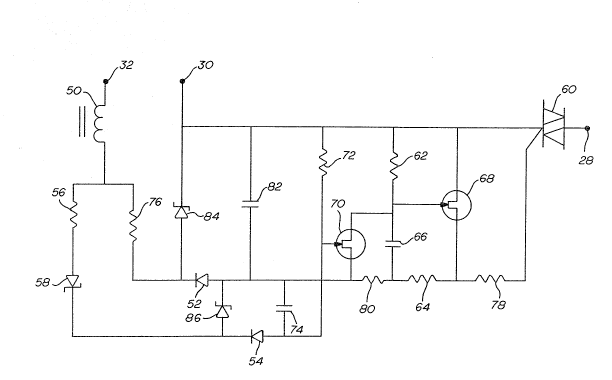
Referring now to Figure 3, shown therein is a circuit
diagram for preferred embodiment of the ignited disabler on the
present invention. The topography is basically the same as in
Figure 2 except for including some circuit details for pratical
CHN-014076 1~ i PATENT
RLM:nls
06/09/B7
RLMP3;b
application. Terminals 32, 30, 28 correspond to the identically
numbered terminals in Ffgures 1 and 2.
The power supply portion of the circuit o~ Fig~re 3
comprises choke 5~ and rectifying diodes 52, 54. Of course, it
0~ should be readily apparent to those skilled in the art that
alternating current dppl~ed across ter~;nals 3~9 30 will be converted
~o direct current by speration of diodes 52, 54.
The ti~e delay initiating portîon, which, as ~entioned
above, performs an AC threshold function9 comprises dropping resistor
56 and zener d1Ode S8.
The sw;tçh portion o~ disabler 12 eomprises a
bi-directiond1 trtode ~hyristor or triac 60. Triac 60 is inserted
between terminal 28 and swi~ch tri3ger portion 46. In ~igure 3> the
swltch tr1gger portion comprises resistor 62, 64, capacttor 66 ~nd
field effect trans;s~or (FET) 68. Those skilled în ehe ar~ will
appreciate ~hat the ~bove-identi~ied components cons~itute a
conventional RC timing network whtch operates in conjunctlon with FET
68 to apply a "trigger" current to the gate of triac 60. In
preferred embodiments o~ ~he present lnvention, Qf whtch the
~mbod;men~ o~ Figure 3 is an axa~ple, built in t~me delay wi11 be
suf~ktent to accommodate momentary interruption o~ power resulting
in l~mp outage. As is ~el1 known to those skilled ~n ~he ~rt, lamp
~nd fixture com~inations, af~er operatin~ fior some time and be~ng
ex~ingu;shed, must coo1 down to a certain d~gree before ~he la~p ts
capable of being reignited. In such hot res~rike circumstances, if
- 12 -
CHN-014076 PATENT
RLM nls
06/09/87
RLMP3:b
sufficient ti~e is not a110wed for the igni~or ~o be in the on ~o~e
during the cool down period, ~he high voltage pulses w;ll cQa~e
before the lamp is capable of reignition resulting ~n lack of lamp
re~trike, The various elements of the circuit depicted in Figure 3
05 are o~ such values and are so operatively connected to provide
sufficient time for hot restrike of lamps.
A secon~ ~ET, designated FET 70, a resistor 72 and a
capacitor 74 combine to form the switch trigger reset portion of the
disabler. As those skilled in ~he art w~ll readily apprecia~e, the
di5charge of timing capacitor 66 is perfor~ed by FET 70. As has been
previous~y mentioned, 1n all previous circui~s serving the purpose of
the circuit of the present invent~on, a bipolar ~ransistor has b~en
us~d to d~scharge timing capacitors. This practice has left a
voltage residue of approxi~ately 0.6 volts in capacltor 66. The use
lS of FET 70 in the c;rcuit of the present inven~ion insures that timing
capacitor 66 discharges to zero volts at all temperatures. A second
aspec~ of the ~bove-described trigger reset por~ion that ~hose
sk~lled in ~he art will readily appreciate is tha~ i~ is elec~rically
incorpora~ed into the circuit shown in Figure 3 so that ~ET 70 resets
or discharges timing capacitor 66 upon sensing of lamp 10 ignition
accamplished based upon vol~age drop across lamp 10 connected a-ross
terminals 30 and 32.
Various other circuit co~ponents, spec~fically, resistors
76, 78, 80, capacitor ~2 and zener diodes 84, 86 are incorporated
into the circuit ~f the preferred embod;ment o~ ~he present invent~on
- 13 -
CHN-014076 ~ 2~4~66 PAT~NT
RLM:nls
06/09/87
RLMP3:b
as position clearly set forth ln Figure 3 where they perform current
resisting, filtering and vol~age limiting funct~ons in well known
m~nner~ fully Ull~ dnd a~precl~tea Dy ~no~e skilled in the art.
By way of example only, a eircuit such as shown in F1gure 3
05 could be construct~d of co~ponents having designations or values as
l~sted below.
~esignation
Element ~umber ~Ye~ or Yalue
Inductor 2~mH
52 ~iode tN4001
54 Diode ~N4001
56 Resistor 1~0K
58 Zener DirJde 75V, 1N5374
Triac T2300B
S2 Resistor lMES
64 Resistor 1.2K
66 Capaci~or 220uf. 10Y
68 ~ET 2N5640
FET 2N3640
72 Resistor 470K
7~ Capaeitor 0.1uf
76 Resistor 5 6~ W
78 Res~stor 220
Resistor 270
82 C~pacitor 220uf, 10Y
84 Zener Diode 6.8V, 1~53~2
~6 Zener Diode 19Y, 1NS3
From the foregoing descrlption and fdentif k~tion o~
eircuit components, ~hose skilled in the art will readily appreoiat~
and understand operatlon of ~he presen~ly preferred embod~ment of the
present inventionO Lamp 10 Yoltage passes through choke 50 which
~ilters the high voltage starting pulses from the 120 V.A.C. present
at that point. Reslstor 76, placed in serles with choke 50, per~orms
A Yaltage dropping and curr~nt limitin~ function ror the negatlve
~ 14 -
CHN-014076 PATENT
RLM:nls ~ f~
06/09/87 ~-~J~ ~ ~ ~'~
RLMP3:b
6 V.D.C. supply. Zener d;ode 849 connected from the end of res;stor
7S to common, limits the voltage ~nd produces a square wave output
p~aked at negative ~.8 ~olts. Thls square wave is cause to flow
through a recti~er diode 52 insuring that only negative voltage is
05 present on fllter capacitor 8~ which is connected fr~m the anode of
diode ~2 to common.
The timing circuit components are resistor 62 in series
wi~h capacitor 66 connec~ed from the com~on to the nega~ive 6 vott
power sUpply line. The common po~nt of the RC timing network is
connected to the gate of FET 68 with the drain and supply ronnections
of FET 6~ going to the co~mon and neyative 6 volt power supply lines.
When power is first applied to the clrcuit the gate of FET 68 is held
low ~nd FET 68 is turned off. As capacitor ~6 charges, ~hrough
current ~low from res~stor 62, FET 68 gate voltage increases until
FET 68 turn5 on, and prevents current ~rom flowing into the gate
terminal of triac 60.
Trid~ 60 c~ntruls the AC power to the lgn1tor 26. Trlac 60
exercises such cDntrol because it is in serles with the ~ommon and
starter conne~tion point 2B as ~epicted in Figure 1. On ini~ial
power up current flows into the gate of triac 60 vla re~ist~rs 7fi, 64
~nd 78 which limit the current. As the timing circuit comes 1nto
effect and FET 68 ~urns on, the triac 60 ga~e current cedses to flow
and triac ~0 turns off preventing starter 26 fr~m-~unctionlng.
9~66~i
The rese-t function is preformed by FET 70. A negative
25 V.D.C. supply, for the reset function, is generated by
dropping the voltage and limiting the current, through the
resistor 56 and the series zener diode 58. The diode 58 also
determines a threshold vo:Ltage under which the reset is
preformed. The voltage is squared by the zener diode 86
connected from the cathode of zener diode 58 to the anode of
diode 52, and then rectified and smoothed by the diode 5~ and
capacitor 74. This negative 25 V.D.C. is connected to the gate
of FET 70 and controls the discharge of timing capacitor 66.
When the negative 25 V.D.C. is not present, which it would not
be when the lamp is operating, resistor 72, connected from the
gate of FET 70 to the common, pulls the gate of FET 70 high,
turning the FET 70 on and discharging or resetting capacitor
66. When the negative 25 V.D.C. is present, as it would be if
the lamp voltage is high or if the lamp is bad or if there is
no lamp, the gate of FET 70 is pulled low turning it off and
allowing capacitor 66 to charge up and perfcrm predetermined
time delay, energi~ing starter 26.
At this point, practical operation of the ignitor
disabler should be readily apparent to those skilled in the
art. For example, when incoporated into or retrofitted in an
igniting and operting circuit for an HPS lamp and a cold start
(lamp) is undertaken, the ignitor disabler will have no effect
and the lamp will start and operate normally. ~nder a cold
start (unlamped~ condition with the ignitor disabler in the
circuit the high voltage pulses will cease after the
predetermined interval. If a lamp is screwed into a
-16-
~ ~.
CHN~014076 ~ G6 PATENT
RLM:nls
0~/09~87
RLMP3:b
receptacle of a fixture under these cond~;on~, the lamp will not
lgnite and it will be n~cessary ~o reset the disabler. Reset under
these conditions would ent~l turning ~he po~er off and on again
which will lead to the lamp ignit~ng and functioning normally. If d
05 short power interruption were to occur, a circui~ having ~he disdbler
wlll extinguish the lamp, and a cool down period of 30 to 60 seconds
will occur before ~he lamp retgnited. This is identtcal to operation
o~ circuits without a disabler installed, as the disabler resets
itsel~ ~u~omatically. If the la~p shall be f~ulty or if a 1amp
parame~ers go beyond the capability of the ballast output, as in the
case of a cycling "end of life" lamp, the disabler will disable the
ignitor and, hence, increase its useful life. In a regular sys~em,
on the other hand, the ~gnitor will con~inue to supply high ~oltage
and rQduce the ignitor's operational life. It ~ay be noted that in
the case of the cycling "end of life" larnp, s~itching the power off
And ~n again resets the dlsabler and th~ la~p will rQignite and run
for a cycle.
With regard to method of l'abrica~ion of a circul~ accord;ng
to the present invent~on, a printed circuit board containing the
circuitry as ~hown in Fi~ure 3 and po~ted in a can approximately
2-1~4 in~hes ti~es 1-1/2 1nche~ times ~-1/4 ~nches oval, wl~h ~hree
leads protruding outside the can ~or connect~ng purposes can be
~onstruct~d by conventiona1 techniques. Further, thP can can be
insul~ted by a polyolef;n heat shrink ~ube to prevent shor~ing to
2~ çurrounding c1rcuitry, also a conventional technique. An alternativ~
,
CHN-014076 ~2~4~6 PAT~NT
RLM;nls
06/09/87
RLMP3:b
construction would be to cast the circui~ board in a potting co~pound
without a sepdrate ~etal can.
A unique aspect of the ignltor disabler ~ the present
invention is its independence fr~m the ballast. ~ecause of this
05 indPpendence, it can be used in conjunc~ion wlth any standard
ballastJ1gnitor currently commercially available with appropriate
adjustment of element values within the disabler. The preferred
embodi~ent of Figure 3 can itself be used on any primary voltage from
12û volts to 600 volts without modification since it derives lts
power from ~he ballast secondary winding which in all cases involvinq
ta~ps of 150 wa~ts or lower is providing the 120 vo1~ open circui~
volta~e dictated by the arc tube voltage req~irement of such la~p5.
Further, in all potent~al embod1ments of the disabler ~f the present
invention, becsuse each ;s a separate unit, each can b~ retrofitted
to any existi~g installa$ion at ~inirnum cost, since the ballast does
not have to be changed to accommodate the funct;on.
~bvious, numerous modifications and ~ariations of the
pre5ent invention are possible in light of the above teachings. For
: exa~ple, in the presently preferred embodiment sw~tch trigger portion46 ~n~ludes an FET 68. This component 68 could be eliminated ln
future preferred e~bodiments of the present invention. Other chanyes
may be made by c~rcuits to work w~th higher wa~tage HPS lamps. I~ is
therefore to be understood that, wlthin ~he scope o~ the appendec;
claims, the preSent invention may be practiced otherwlse in a
specifical1y descrlbcd hereinabove.
.. 18 -
,, ,~