Note: Descriptions are shown in the official language in which they were submitted.
6~
- 1 - 61051-2231
10 GIGASAMPLE/SEC TWO-STAGE ANALOG STORAGE
I~TEGRATED CIRCUIT FOR TRANSIENT
DIGITIZING AND IMAGING OSCILLOGRAPHY
Cross Reference to Related Application
A high speed analog signal sampling circuit is shown in
U.S. patent number 4,811,2~5 by two of -the inventors named here-
in.
Background of the Invention
This invention is directed generally to an analog stor-
age device and more particularly to a device for very high speedsampling of analog pulse information.
There is a great need to e~tend the range of measurement
capabilities of high speed, very short lived electrical phenomena.
Such measurements are particularly important in the growing fields
of laser communications research, laser fusion energy research,
nuclear research, weapons study, and high speed imaging. Other
possible applications include biological research, materials re-
search, and accelerator and high energy physics research. Transi-
ent digitizing techniques are already in use in most of these
areas. However, in known systems, the accuracy degrades signifi-
cantly with increases in transient speed of the signal to be
sampled.
Prior efforts in this field have been limited by the
fact that the storage capacitor for storing the signal sample must
be kept extremely small, rendering it highly susceptible to leak-
age which degrades the accuracy of the sample. Moreover, because
of the small siæe of the capacitor, the sample can only be held
for a very short time.
-2
~ urther limika~ion o~ known ayE;tem~ in the ~ield is
that they ~re r~ot ~d~ptable to slmultnneou~ reading of a
plurallky of ~imul~aneouE;ly occurring ~ign~16.
Current: l~own D~ethod~ are limit~d to ~amplln~ ~peeds of
S about 100 MH~ with accuracie~ o~ 6-~ bit~. ~e~e de~fices,
:known a~; fla6h ~n2l10sito-digital converter~ (~DCs), are
expen~ive, c:on~ume hlgh power, ~nd reguire high 6peed,
gh power ~nd exp~nsive ~e~norie~ r d~ta storage . Dual
range t~chnlqueE; tc> ~ncreas~ 'che ~Icc~aracy beyond eight
10 bit~; becDme ~pproximat~ly twice ~s expen6ive.
Summ~ ry of t21e InventiQEI
It iB an objectiv~ thi6 invention to provide a system
c:apable of 6igni~icantly improved ~ampling of fa~t pulse
~ignalfi in a ~res~uency r~nge and ~1: a ~ampling ~peed use-
15 ~ul ~ n laser rlnd nuc:lear research and de~r~lopment, s~ommu-
nications, imag~ ny and other purpo es .
A $urth~r objec:tive herein ~s to provide reduced per-
ch~nnel cc~t~ in high 6peed ~ampling applications,
especially where ~ultipl~ channel~ must be simultaneously
20 ~ampled.
a ~Eurther l~b~ ectiv~ to provide improved dens ity ~nd
power con~umptic~n ~rl an ultra-hi gh ~apeed ~ampl ing
circuit, ~aking f~a~ible very large multi-channel ~rrays.
Mor~ part~cul~s~ly, ~n e~bjective herein i5 to providl~ a
25 ~ampling 6p6~ed ~ncrease ov~r current pul~e campling
circuit technolo0ie~ of approacim~tely 100 ~i~es (twt~
- order6 of ~gr~itude~ ~or 3hort durat~t7n pulse ~vents.
1~ ~urther ab~ec~ve her~n i~ to prc~vide ~ ~ignal Gampl-
~ng devi~e capa}:)le o~ ~ ~and width of gre~ater than one
30 G~z at 3~b r~ f f .
5 ~ 1 0/3~S
67~
--3--
Another o~ectiv~ her0~n iB to prov~de an amplitude
aocuracy ial~provement over current ~la6h ~DCs cf 1-1/2
ord~r6 of ~agnitud~ ~or the basic d~vi~e ~lD bi'cs com
par~d with Ei~ x bitE~; O.1~6 cf 1. 5% for full ~c~le) .
5 A further ~nd related objective her~in i~ to provide a
high 6peed E~am~ling Bevice which cc~n~u~es low power and
has a r~ tively low co~t per channel.
A furtller objective hea:ein i6 to pro~ide an ~ntegrated
circuit 31evice h~ring as~ ective and efficient multiple
10 chann~l capability ~or bein~ adapted to two- or three-
di:~er~sional 6ampling ~rrays~
A ~urth~r obj ectiv~ l~erein i 6 to provide a high peed
digitizing circuit that can be easily reconfigured for
longer ~torage time interv~ nd which further includes
15 a reprogra~nakle ~a~pling rate for daptation to a wide
range o~ E;ignal frequencies.
The rec:onflgurable ~igh density and low cost ~eatures of
thie invention allow the device to be adapted for ~uch
applic~tion~ a8 recording of ~ingle transient phenome~a
;~o for extended peri~d~ o~ ti~e; generation o~ ~ stored
ocsillo~cope di~play; ~3~pu~er stor~ge of hundreds ~r
thoucand~ of channel~ v~ related or independent data; ~r
generation o~ hlgh ~pead, hiyh r~salution graphics or
related picture ~tor~ge ~y6te~s wi~h aper~ure ~imes of
~pproxi~ately 0~1 n~no~e~ond~ per pho~ograph ~nd pic~ure
r~t~ Df 101~ per ~c~n~.
In thi6 invention, it ha6 ~een re~ognized that a large
~d ~xtre~ely ~portant ~la~s of ov~nts s~guire only that
:the~e ~xtr~ely ~6t pheno~ena ~e observ~d ~r a ~hort
~riod o~ time. Thi~ ~vorable duty cycle l~nds itself
to t~e invention t~ be ~escri~ad. Some circu~stances
will r~guire t~e ob~erva~ion o ~ny such signals
A-45210fJAS
7~i
--4--
61multz~nee:>u61y, or o:~ certain eignal~ over a ~ore extend
~d p~rlod of time. ~gain, the invention to be described
c:an be configured to addre66 these l;pecial requir~ments.
In 6umm3~ry, the invention compri~e6 ~n analc~g $ntegrated
5 eircuit uE;ing ~nte~rated ~ield e~fect ~ran~ tor techno-
logy co~npri~ ng ~ plurality ~E 6ampling ar: d 6torage
~ells. To achieve t,he high speed p~rf~ nce required, a
twc>- taç~ ampling cell de~;ign i6 u~;led. The fir~t ~tage
inc~ rat~6 a very 6mall capacitor coupled to the input
10 ~ignal tl~rough a l~lgh ~peed gate. This gate, which is
~p~ned only ~y the ~imultanec>u~ occurrence of row ~nd
column ~ell~ ~Ln the circuit, cau~;e~; tl~i~ fir~k capacitor
to capture ~t very 21igh ~peed ~ ~ample of the analog
~ignal under stu~y. When a~l the ~ir~t capture ~ections
15 oP the c:ell haYe captured on their capacitc)r~ a ~ample of
the analc~ signal, a tranc:f~r qate is briefly opened to
transfer th~ captur~d and buf~ered ~ample values to the
second or storag~ E~ect~on of the c:ells. Thi~ E;t~rage
~ection incorpora~tes ~ capacitor E~ub6tantially larger
20 than the s:apacitor ~n the capture ~ec'cion, ~nd capable of
6torlng the 6ignal for a ~on~iderably longer tiDle.
Th~ ~torage ~ectiorl~ ar~ read out in ~ multiplex~d fash~
ion through ~n output bu~r ~:omprl~ing a pair of ~natched
tran61etors ~oeding ~n analog output ~pli:fier. The out-
25 put a~pli~ er i6 d~signed to provid~ voltag~ ~eedback toone of 'che two ~atch~d tran~i~tor6 o~ t~e output buffer
~o th~t nc~n-linear~ti~s ~r~ remov~d from lthe 6ignal
rapre~enting the ~ctuaï output whi ::h is read by tha tran-
tor fro~ th~ ~torage cap~citor; ~nwhile, the n~n-
30 destructivc~ readc~ut format iB ~aintained. Further, byUBe ~f the ~eparate output 3bu~Eer in co~nbln~til~n with a
~3taged ~torzlg6~ ~ection/ th~ r~ad ir~ and r~zld-out 3l~0d~s of
the c~ll nre s~parated, and could ~unction ~i~nultane~usly
if dl~ired,
1~-4 5 21 OJJAS
61051-2231 VM:lad
The cells are assembled on integrated circuit chips
comprising in a preferred embodiment 1024 (32x32) storage cells.
A further novel feature herein is that various arranyements of the
inputæ can be made to extend the captured record length, both
horizontally in terms of the number of channels being sampled, and
vertically in terms of the length of the record. Because of the
extremely low inpu~ capacitance of a given column of cells, it is
practical to combine cell groupings either vertically to add
additional devices, or horizontally to columns of devices, to
achieve sampling groupings that are extremely flexible and can be
more easily tailored to a particular application. Thls
flexibility is of paramount importance in certain applications
where many thousands of parallel data channels must be
instrumented. The high speed timing required to allow the
coupling of different portions of the same signal to a single
channel or adjacent channels is achieved either through the use of
delay lines, the delay lines being used to delay the input of the
analog signal being sampled to the next adjacent chann~l; or by
application of a ga~ing signal to the capture section of a cell
v~a a high-speed parallel output shift register, or equivalent
timing technique.
In accordance with a broad aspect of the invention ther~
is provided a high speed data acquisition system for storing a
succession of sampled values of an analog signal compri~ing analo~
signal input means and analog signal ou~put means, a first analog
bus connected to said input means and a second analog bus
connected to sald output means, a storage array comprising a
7~i
5a 61051-2231 VM:lad
plurality of cells arranged in rows and columns, row clock means
coupled to said array for selectively activating each row of said
array, column cloc]c means coupled to said array for selectively
activating each column of said array, said analog signal beiny
directly coupled to said array to supply said signal to the cells
of said array, each of said cells comprising a first, capture
section responsive to said row and column clock means for
capturing one of said sample values at high speed~ a storage
sec~ion for holding said captured sample value for a relatively
lonyer perlod ~han said capture section, an output buffer for
transferring said captured sample ~o said analog signal output
means, and transfer means for transferring said captured sample
from said cap~ure section to said storage section, whereby a very
high speed sample of said analog signal may be taken by said
capture section, said sample thereafter being transferred to said
storage section.
BrieE Descrip~ion of the Drawings
The details and advantayes of this invention will become
apparent to a person of skill in the art who studies the following
description of a preferred embodiment given in conjunction with
the following figures, which comprise:
Figure 1 is a detailed schematic view of the two-staye
sampler and output buffer design;
Figure 2 is a timing diayram illustratiny the signal to
: be sampled and the timing signals needed to æample this inpu~
signal;
--6--
FIG 3 ~llu~;trate~; ~n alternative ~rr~y of timing 6ignals
u~able with th~ nt c~f FIG 1 tc) 6ample the analog
input ~ignal;
FIG 4 ic; ~ 6chematic diagram of the output buffer and
5 output ampl~ r 6ehem~ u6ed to linearize the output data
of the ~a~npling cell;
FIG 5 i~ a ~chem~tic diagr~m of a driver circuit used to
drive on~ o~ th~ cc)rltrol gates o~ the capture ~ection and
having ~n extre~ely rapidly ~alling l:railing ~dge for
lo ~ontrolling the ~ste:
FIG 6 illustrat~ the ba6ic ~rranqe~ent of a plurality of
input cell~ arrayed ln colu~ns to sample a plur~lity of
~eparate input 6ignal~;
FIG 7 illu~tr~tes an alt~rn~tiYe to FIG 6 in which the
15 array of 1024 cellæ Dl~y be uE;ed to ~ample a ~ir,gle input
signal Vl;
FIG 8 illustrates ~n alternative arrangement in which an
entire integrated chip of 1024 eells ~s used to E;ample
four ~nput 6ignals Vl-V4:
20 FIG 9 illustr~te6 an ~rrangement lncorporating alterna-
I:ive u~es of delay llnes to delay ~pplication o~ the
input ~ignal . r the cll~ck E~ignal to columns s~f cells in
order 'co ~i~plify the gener~tion ~f timing ~ignal~; nnd
FIG 10 illustr~tes an alternative arr~ngement incorporat-
25 ing a plurality of int~gratsd clrcui'c chips ~ach compris-
lng 1~)2~ C~ 6, the data or clock ~ignal~ being delaye~
~y ~ppropriately Gc~nne~ed del~y lineE; ~r ~ r delay
device to captur~ ~ ~equenc~ OI ~amples of ~n analog
~ignal over an extended period o~ ti~e.
A-4 521 0/JAS
6'~
--7~
Detail~d Descrip~ion of a Preferred Embodiment
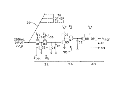
The tw~;ct~e c~11 de~ gn 20 u~ed tc: ~;ampl~ an analog
signal lnput V~ hown in schemat~ rm in FIG 1.
~his ~mpling ~ell 20, which ~ clude~ ~irst ~nd ~econd
5 6tages co:mpri~ing a t:apture ~;tage 22 and ~ etor~ge 6tage
24 opt~m~ ze6 the ~peed o~ sampling. q~e go~ f th~
I;amplins~ design 1~ to ach~eve el circui~ lnput band width
of great~r than 1 G;Hz ~ ~nd ~ampling ~peed~ of up to 10
GHz (10 gigasa~ple~/6ec, sr GS/6). TAe æpe~d of the
lo basic c:ircuit is~pl~!sment~tibn to b~ de~t~ribed i5 limited
only by th~ input-~Eollowing ti~e c~nE;tant which defines
the bandwidth, and ~y t~e external fa . t ti~lng circuitry
(which will be de6crib~d with respect to FIG 5~ which
mu~t generate elean ~ign~l~ of 1 nanc~econd tr~nsition
15 time ~or optimum perf~rmance ~t ~ 1 GS/~ r~te in the
current iD}: lementation .
The principle l~f operation OI the basic 6ampling cell is
a_ ~ollows: the analog SIGNAL IN (V; ahown also ~t the
tQp line ~f FIG 2~ pplied t~ the input of the 6amp-
20 ling cell~; 20 through a c~ n anal~ bus 30 on the
~nt~grated circuit chip that will carry a large num~er of
the cell~, typically 1024 per chip. ~he typical ~inglo
6ampling oell 20 co~pri~es two ~t~ge~ he first, called
the eignal s:apture 6;~ct~sn 22, ~ncludes es~entially a
25 pair o~ FET s~ates Ql, Q3 ~ollowed by a ~mall ~ampling
o~pacitor Cl. This c~pacitos Cl ha~ ~n extremely small
value, ~nd 311~y s~entially c:o~nprise only the s . ray capa-
citance ~f th~ input circuit. The reason for the use of
ry low v~lue c~paci1:ance i~ ~:o reduce ~he input
30 capacit~nce c~f the Ga~plinçl ce~ll 20, m~xiD~izing the speed
of 6ampling and the nu~iber of ~11G th~t ~y be connected
tc~ the co~non bu~ 30. ~or optiYnum bandwid~t~, the voltage
~ollowing RC time con~tant 3~11St be very ~hort; therefore,
a pr~ferred ~ dilDent o~ the desiqn ~or capacitor Cl
35 ~nini~izes the v~lue l:o approxi~nately 0.1 plcofarads, so
A-4 S 21 O~JAS
6t;~
~B -
tA~t the ~e tlme c~n~tant become~ ~pproximately lO0 pico-
seconds, leading to an input bandw~ dth o~ 1. 6 GHz .
I'h~ storage ~apa~it~r Cl ~ buffered by a voltaye follow-
~r circuit 32 rompri~ing ~ palr o~ FET6 QS ~nd Q6. In an
5 ~lternatiYe embc~dixaent, the buiE~er eir~u$t 32 ~nay be
repla~ed wilth a stag~ providlng voltage qain. l:ach sam-
pling cell 20 i5 activated ~y the ~:oincid~nt ~ccurrence
o~ ~ pair ~r sign~ F~ and ~C~ (FIG 2t lin2s 21, 23),
applied t~ g~teE3 34, 36 o~ ~he pair o~ ~ran6iE;tors Ql and
lO Q3 . Typic~lly, the column si~rlal ~e ~ r~mains on for the
entirçs ti~e a colu~ c~ ~ell~ i B to be ~nabled. The fast
gate oontrol ~;lgnalE~ applied to the gate 34 c~f transistor
Ql are gener~t~d ~ hip ~preferably u~ing the circuit
of FIG 5) and c~u e lthe ~torlng oP a value of ~ p;~rtiru
15 lar v~ltage taken fr~m the ~nalog 6ignal ~ nt the occur-
rence of ~he traili~g edge o~ ~he ~t~rage g~te wavef~rm
~Fi . The capture ~ection 22 in ::ludes two ~urther tran-
6i~tor~ Q2 ~nd Q4, ~dh~6e ~unction~ contribute to the
~sccura~y o~ capture Istage 22, and the ~ccuracy of
20 tran~fer of the captured E;a~ple to the next eucceeding
~torage stage 2~a. Tran~i6tor Q~, coupled between the
~unctlon of transi6t0rs Ql and Q3 and controlled by
~ignal INH (FIG 2 f llne 25) ~ GOC~p~rateS wlth tr~nsi~tor Ql
to for~ cer ~gain~ unwanted 6ign~1 eed l:hrough
25 during reaa-~ut oi~ the data. Low requency nc~ise ignals
ill be attenu~ted in the r~tio f R2on/ lof~
frequency eed lthrough will b~ ited by ~l~e at~enuation
f~tor o~E Z;2on~Xlo~, where Xl ~ primarily the reac-
tanc~ OI 'c~le ~l:ray c~p~cltance fro:m the input to the
30 ~unction of t21 ~nd Q3. ~ransi~tor Q4 is coupled between
the junct~ on of tr~n~istor Q3 ~nd capac:itor Cl, ~nd
grc~und, ~t~ ~t~te b~lng cvntroll~d by the ~ign~ (FIG
2,11n~ 27)o As ~ppear~ at th~ bot~om o~ FIC 2, th~ state
o~ ~ign~l ~R is c:h~nged to 5~round cap~ci~ r Cl, discharg-
35 ing it co~pletely. Tran~i6tor ~24, togeth~r wi~h
A 4 5210/JA5
~9--
tran~ or Q3, t~us ~orms ~ E~econd ~ilter to isolatenoi~e ~rom re~dinsll thf3 6ample ~n C2.
In 6u~nmary, ~ample~ of the ~IGN~ IN V~ ar~ taken at the
trailing edqe o~ e~ h ~a6t yate E~ignal ~F L appl~ ed to the
5 gate of tran~tor Ql and stored on cap~c:$tor Cl. 5ince
cap~citor Cl iE~ v~ry 6mall, ~te hold ti~ue ~ 6 liT~ited to
v~ hr~x~ ti~e~; o~ the order o~ ~ ~ew hundred ~nicro-
~econds. ~rherefors~ the 6ample ~ell 20 of thi~ invention
compr~e~ a 6econd stage or oe~torzlge ~ection 24 immediate-
lo ly ~ollowing the fir~i;t l;ta~e c:omprising ~ate Q7 activatedby a ~ignal ~T ~nd a l~rs~er l3torage capacitor C2 which
ha~ a v~lue ~ approximately 1 pi:ofarad. ~his l;~orage
~ectic~n 24 provides ~ Estoras~e time for the ~ample cell 2 0
of hundreds o:f ~illi6e~:Qnds. It ean be ~een from FIG 2
15 l:hat the tr~nsfe3: gate, co~pri6ing i:rarlsi~t~r Q7, is
enabled ~y the signal ~T ~at ~ tiDle following the fast
~ate signal ~ to the tran6isltor Ql of the last ~ampling
cell 20 of an ~rray. Thif~ way, ~11 the data or ~naloq
~a:nples ~tored on the ::apacitor Cl o~ ~very cell 20 are
20 trarl~ferr~d simultaneously to the ~torage ~tages ~4 and
speci~ically the cApacitcr6 C2. It $s ~ ~eature o~ this
invention that at the ti~ne T2 (FIG 2, l~ne 27) when the
~ata ~re tran6ferred ~ro~n ~2e capture ~ection 2 to the
~tora~ ~e~tlon 24, ~nother ~a~t write cyc:le ca~ imm~di-
25 ~tely c:~D~e~lce ~ven ~hile the original data is not yetread ~ut or ~B l:~eing read out v~ th~ laultiplexed read
lines 4~, 44. Thu~, ~ double ~hot ~East c:~pture ~ode is
po~ible, ~o long as the ~rst ~at~ ~a~ple transferred to
th~ storage ~tag~ c~pflcitor C2 ie r~3ad out rapidly ~nough
30 that tl~a dynamically ~tored data th~ t~red in l:he
~econ~ rs:und c~f dalt~ nple~ on ~e ~:~pture ~;tage capaci-
tor C~ ~e not siyn~ antly deteriorate ~efor~ transfer
of the ~ec~nd ~ pl~ ~Lnl:t~ the ~econd ~tage ~torage
capacitor C2.
A-4 521 0/JAS
The Btorage ti;ne extQnsion provided by the ~toragP 6tage
24 i3 particularly ~mportant ~Ln typical imple~entations
b~here lergla array~ o~ c:ell~ are to be read out over a
c~on analog 3: u~ a~ ~ill be di6cuss2~ ~ith respect to
~IG 10. Capacitor C2 of the ~torag~ 6tage 24 $a followed
by ~n output buf ~r 5't:~gç3 40 compri~ing a 1:ransi~tsr Q8
operating in oon~unction with ~ r~fer~nce cell Q9 to
~rovide a dlf~Eer~ntial zmal~g read-out ~ignal cor,sisting
OI the ~;alopled voltage and the reference voltzlge impress-
lo ed upon di~feren~ial analog outpuk buses 42, 4d,. This
operation will be axplaill6ad in greater detail below.
A ~llrther impo:rtant ~eature of the desi~n of the 6ampling
~:ell of ~lG 1 is it~ adaptability to ~ontrol by the over-
lapping ti~ing l?ul~e~ shD~m ~or exa~nple in FIG 3. ~s
discussed abov~, the ga~e of tran6i~tor ~21 which controls
the 6ampling of the analo~ s;ignal V~ causes the F~ample to
be takerl upon the c~ccurrence of the trailing ~dge of the
control ~ignal 4F; at gate 34. Bec~use of thi~ and th~
further *act that the length of time for which lthe ~teady
E;~ate of ~he 6ignal ~Fi to any ç~ate 34 may ~xi~t is not
relevallt to the 6a~ple time, a ~erie~ of overlapping
timing signal6 s~uch a~ thD6e hc)wrl ~n FIG 3 and labelled
60, 62, ~4 ~ay be ~ppli~ad to the gate~ of the transistors
Ql or a plurality o~ 6~epar te ~:~116 that are receiving
the 6a~e input ~lgnal Vl, 65. It ~an be seen in FIG 3
that 6ignals ~50, 62, 64 ~er~selves overlap, but that the
trailing edges thereo~ are 6~parated by per~aps 100 pico-
6econd~ . Thus in l:he ~x~mpl~ 6hown ~n ~IG 3 J 10 adj acent
~ell~ at once could be ~urned on and actively trac~ing
- 30 and ~a2npllnsl the input vDltage w~lveform. The actual sam-
ples wc~uld b~ t~kerl ~t ~e trailing edges o:E th~ contr~l
~ignal~ 60-64, which edges eBn be very C:lQg~ly ~paced in
ti~e. B~csu~e s~ v~ry ~all cap~ei~ance of the
c~pture ~Itage . apacitc~r Cl, the input i~ loaded Dnly very
3s ~lightly ~Dore than i~ would be n~ally. In contrast,
no~lly the input capacitance to ~ large csll~ction OI
A-4 5 21 0/JAS
~ 61051-2h31
cells would be very large compared with the inpu~ capacitance of a
single cell. Thls advantage is achieved in part because each
cap-ture stage 22 o-f this cell design 20 is isolated by the input
FET gate Ql, so that the input capacitance is limited to being
essen-tially the capacitance of the channel of the F~T Ql itself.
Turning to FIG. 4, the dif-ferential read-out scheme of
this invention is shown in detail therein. To read out the volt-
age stored in any sampling cell 20, -the particular cell is select-
ed by the multiplexing yate 70 in a manner already known in this
technology and described for example in the abovementioned U.S.
patent 4,811,285.
The multiplexed differential output signals 72, 74 are
fed through a pair of operational amplifiers 76, 78 into a voltage
sensitive high gain operational amplifier 80. The output of this
amplifier 80 is read as the output signal VouT of the samp-
ling cell and is applied as a feedback signa] VREF to the
gate of transistor Q9 through a filter section (not shown). By
this feedback action, the current difference between transistor Q8
(which provides the actual stored sample from storage section 24)
and transistor Q9 (which comprises the reference transistor) is
minimized or nulled to a fraction of the sampled voltage, that
fraction being defined by the ratio of the closed loop to the open
loop gain as in any known feedback circuit. The transistors Q8
and Q9 are of matched monolithic construction to minimize differ-
ences between the reference signal 72 and output sample 74. The
amplifier 80 is a high gain amplifier that can be adjusted to
minimize the error in matching the currents from Q8 and Q9. The
result of this is that a linear transfer is provided -from the
capacitor C2 to the voltage output VREF, with any non-
linearities in the operating characteristic curve of the transis-
tors being clivided by
--12
the ~orward gain of the ampli~i~r to reduce their ~igni-
nce.
E~y providins~ the operatio~l a3nplifier~ 76, 78, and 80,
between the ou1:pu~ buffer ~n~ the ~gnal output, and
S ~eedinç~ ~utput E~ l VREF bacX to the ~tched trarl istor
Q9, the volt~e th~t appear~ ~t the gate af the FET
~uf~er tran~$;tor ~29 will b~ ~dent1cal to lthe voltage
re6iding on thQ ~mpling ~ap~citor e2 ~ att~ched to the
galt~ 3f FET bu~fer trAn~i6tor Q~. Transist~r6 Q8 and Q9
10 ar~ identical in ~tructure and very clo~ely coupled
phy6~ cally a~ are the ~ sequent differential pairs of
tran~i~tor~ inc:orporated $n the ~nultiplexing read~ c:ut
bu~;~s. Ther~fore, t~e diæclosed de~ gn will provide a
clo~e tracking ~etween the ~utput volt~ge VOUT of the
15 circuit whlch i6 nc~w t~e re~erence Yolt~ge, VREF, and the
sa~npled 6ignal vc~ltage, to a first order. This unique
read-out ~nethcsd removes the need for ~ir6t order lineari-
~ati~n ~f the data to c:ompensate fc~r the inherent non-
l~nearitie~ in non-fed-back circuits. Correcticn o~ ~am-
20 pled data ~or other erfacts, uch ~s timing and thresholdvariations in the rell6, which are second order effects
lmp~rt~nt only at the highest frequency of operation, can
6t:ill be applied by ~axternal c~libration correction means
th~'c will l:e ~e~cribed l~ter. ~r many ~pplications, the
25 simpl~ lin~arization provided by th~ operational amplifi-
~r ~eedb~ck ~cheme of this invention will be ~ufficient.
Returnia~g to th~a ~ample ce~ll 20, and ~;p@cl flcally the
capture ~ect~on 22, the dri~er Girc:uit ~hown in FIG 5 f~r
providing the ~aet gate pulses ~ Fl to the ga~e of tran-
30 ~i~t~r Ql ~ill next be di~u~;ed. The aperlture, or turrl-
o~f ti~e o~ ~i6 fir~t ~t~ge c~f th~ ~ampl~r t:ircuit i5
cr~t~c~ e tran~l~tor Ql used to prov~de ~i~ gat~ is
~ ~inimwD geo~etry dQvice to op~imize itB ~p~ed s:~f opera-
tion. ~ a~ple ti~e o~ cell 20 iE~ a direc~ ~unction of
35 the ~lling ~dge ti~e of th~ siqnal ~Fi ~hown at the
A-45210/JAS
7~
~13-
upp~r righ~ of F~ 5 which ~rive~ th~ transistor Ql in
FIG 1. I~ thi~ ~dge wer~ ~n~inite6imally short in time,
the ~vice would ~a~ple precl~ely the voltage ~tored on
the c~pacitor at that ti~. At a ~mplin~ 6peed of 1
S ~Hz, it i~ de~ir~ble to have a trailing ~dg~ tlme of 100
pic~second6 or 1~
In a typ~cal ~mplementati~n, ~roups of cell~ will be
connected t~get~er ln a colu~n ~r row array to minimize
the ~m4unt of A~t drive circuitry that must be provided
lo ~or ~he c~ ample lines. ~wev~r~ thi~ increases the
capacitance of the load to be dr~ven by th~ driYer cir-
cuit. FlG 5 ~how~ a driv~r circuit capabl~ of driving up
to 32 e~ w~th ~ ~ignal ~Fi having a trailing or
falling edge time o le~s than 10~ pico~econds, although
15 together, the cell~ h~ve ~ calculated load capacitance of
three picofarads. The design ~s~u~ption ~or this circuit
i~ that the ri~ing adye of the ~Fi pul~e does not need to
be nearly a~ fa~t; ~ut ~ust ~e above a de~in~d threshGld
a ~u~ nt time for the ~ignal to ~ttle to the correct
20 v~lue on the 0.1 plco~arad captur~ capacitor Cl. In ~act,
the ~ignal ~Fi, and therefore the c~pture ~t~ge transis-
tor Ql, coul~ th~or~tic~lly be turn~d ~n an arbitrarily
long time ~head o~ the ~alling ¢~ge. In practice, a f~s
6a~pli~g pul6e ~Fi ~ ~ev~ral nano6~conds i8 ~dvantage-
ous. In e~th~r case, th~ ~ajor require~ent i~ to gener-
ate ~n extre~ely ~a~t ~alling edg~ ~or the ~ignal ~F. A
circuit ~hat 6~rves ~he purpo~e o~ providing the fast
falling ~dga i~r ~h~ signal ~Fi i~ ~h~wn in ~G 5. ~his
circuit ~um~ ~hat ~n input ~ignal 37 comprising a 1
nano~e~ond wide pulse w$t~ ri~e and all ~imes vf ~pprox-
imately 100 p~co~e~nd6 ~nd having an 3utput value that
v~ri~ ~e~w~en -.B v~lt~ ~nd ;;1.~ volt6 i~ gen~r~ed ~rom
~ ~a6t b~p~lar ~r galliu~ aræenide ~h~ r~ r, delay
llne, or an ~gually ~a~t ~urce, rQpre~en~ad by the tran-
3s ~i~tor ~nd r~gi6t~r co~bination labell~d ~L ~vurce 89.~he ~t~nd~rd logie 1~Y~16 0~ ~it~r coupled loqic ~ECL)
A-45210~JAS
L~ 6 ~7 5
~14 ~
are a~u~ned ~or th~ urt:e. Th~ dris~er circuit 90, which
ie ta tA~Ce th~ plllBI~ 87 and sh~pe it to pr~vide the ri6e
and especi~lly t~e ~lling edç~e ti~ne r~guired ~or ~ gnal
jlF~ o~ c:ell 20 ~ ntl~lly c~mpri6e~ a c:ommon ~mitt~r
5 current swit/::h Q91, ~ollow~d by a common ~:ollQc'c~r 6ta~e
Q95 whioh ~un~tios~e 3e ~ c:urrent ~ult~plier. This
current ~nultiplier Q9~ re6p~nd6 to a chang~ ln t~e level
applied ~ECL ~ignal ~7 ~o produ~e a ver~ high
current c:>utput to ~very rapidly disch~rge the load capaci
tanc~ CL 97 of the 6~mple c~ll 20. In this way, when the
OUtpllt 98, which i~ c:oupl~d to the gake of tr~n~ixtor Ql,
chaslg~s ~t~te ~nd provid~s thiE; high s:urren$ outpu1:, an
extre~ely ~a~t ~alling edge of the ~ignal ~Fi ~ prGduced
to provide the le6~ ~han 100 p~c~ on~ f~lling edge
~i~n~l regu~red. The requir~msnt ~mp~sed on the driver
circuit of FI~ 5 i6 to first ~harge th~ capacitor CL
repre~enting the gate cir~uit6, ~nd ~hen to diecharge it
rapidly within the reguireB ~all ti~e. Therefore, a PNP
follower circu~t i6 u6ed inco~p~rating the transistor
20 Q95. The ~witch Q91 1~ d~sign~d ~or a 6t nding current
of 15 ~A. Matching dio~e~ D99 and D100 are provided to
de~ine the range o~ ~ignal applied to the base o~ thP
tran~i6tor ~95. The circuit is designed to oper~te ~s
~ollows: when the valu~ of ~ign~l 87 ~n lin~ 88 t~ the
2s ba~e of ~ran~i~tor Q91 $~ at .8 Y~lts, a 6ufficient
voltage ~rop ~xist6 ~ero~ re~i~tor R92 ~uch that di~de
D100 will turn on, wi~h its ~paed o~ turn-on depending on
~he ~$ze of R92. It haG ~een d~terminsd that this
res$~tor ~hould b~ ~t l~a~t ~00 ~s. At thi6 ti~e, the
33 ollow~r tran~istor Q~5 will ~urn on, providing ~ logio
zero at it~ er output. ~h~n ~he ~ignal on line ~
~o~s to it~ v~lue of -1.6 volt~, t~e colle~t~r of the
tr~n~istor Q91 will ~o positiv~, and ~he ~ode ~99 will
~onduct, ~u~ln~ ~h~ ba~a ~ ~ransie~or ~95 ~o ~o p~si-
tive to ~ut ~.3 v~lt~. T~i~ will cau~Q t~e output att~ ~itter o~ tr~n~tor Q95 t~ ~o po~itlv~, ~nd charg~
t~ ~f~ctive ~apacit~nce CL97 o~ th~ ~ample c~ll with a
~-45210/J~S
'7S
61051-~231 V21:lad
time constant in the up direction set by the values of the
resistors R92 and R102. R102 is typically 300 ohms or less,
assuming a capacitive load of three picofarads.
It is noted that this will lead to a standing current in
transistors Q90 and Q95 of about 35 milliamps, and a combined
power dissipation of 195 milliwatts for one stage or 6.4 watts for
32 stages. To reduce this power, the values of R1 and R2 can be
increased, and a correspondingly longer charging time allowed.
The values shown are quiescent nominal currents. The width of the
clock pulses varied inversely with this nominal current.
At the critical time when the fast falling edge of ~Fi
is to be produced, the signal on line 88 returns to its value of
-.8 volt. Both transistor Q91 and Q95 are configured to be able
to draw maximum instantaneous current in the negative going
direction at this time. Therefore, the fall time at the output of
transistor Q95 is determined solely by the maximum instantaneous
current and the load capacitance CL 97. To get added pull down
current through the transistor Q95, a speed-up capacitor C104 is
provided at the emltter of transistor Q91 to pull added charge
into the base of transistor Q95. This current, when amplified, i5
available to aid in the discharge of the capacitor CL97 and
provide an instantaneous chanye in the value of the current in Q95
a shown at curve 105 on the right of Figure 5.
For transistors Q91 and Q95 to switch sufficiently
rapidly, transistors with an Ft of at least 6 GHz must be
provided; to discharge CL97 in less than 100 picoseconds requires
an instantaneous current in the transistor Q91 of Cdv/dt=100
67~i
15a 61051-2231 VM:lad
milliamps, a very reasonable value.
Diode D100 is to prevent transistor Q91 from saturating,
and guarantees a stable low level voltage at the output of
transistor Q95 at the zero voltage conditlon. Diode D99 prevents
transistor Q95 from turning off, and sets
7~ii
--~6--
'che high 1~3~rel at the l~utput of tran~i~tor Q95 to 4 . 3
volt6. ~n ~ddit~e~nal diode D106 1~ provlded across the
ba6s e~nitter ~unct~on of transistor Q95 t~ prevent
potential damaSIe to this tran6i~tor~
It Ishould b~ noted that to prevent ~xcess power dissipa
t~n in th~ circui~ n option to pul~e 'che supply
power ON ~uet befc~re c~mencem~nt o~ the write ycle. In
many application~, thil!s '16 ~!1 per~ec:tly accepitable mode of
operation. 1~,16t~ o increase th~ gate transition, and
hence, improve the dyrlamic: range, the ~upply pc~wer for
the buffer ~3e~tion ~ust d~cribed c:2n be pulsed to 2
60m~what higher level ~6 volts) shown in FIG 5.
The driver c:ircuit described zlbove i6 a c:lear improvemen~
over kncn,m driver circuit6 in that the pc~wer dissipation
1S iE~ c~ntroll~ble ~y :reduc~ng standing ourrent at the c~st
oî ch~rging the ~witching circuit~ ~ore ~l~wly. The max-
imum speed of the falling edge i~ preserv~d by virtue of
Ith~ hl gh c:urrent gain of bc~th transi6tor~ Q91 and Q95
being u~ed to drive the discharge of the c~pac:itor CL97.
W~th ~ppropriate external control circuitry, having
prc~pagation delay relakively les~ than 100 picoseconds,
groups of cell6, ~.g., columns, or ~ntire chips can be
phased to achleva asl overall 6y6tem 6ampliny rate of up
~:4 1 O GS/Bec-
Havlrtg d~rri~ed the organi zatis~n and design of each
e~ll, the r~maining figure~ ~llu61trate dif~erent ~D~IIS of
~rgnni~ation ~n a ~ingle chip of ~ plurality o~ gro5 ps of
In ~n exemplary embodiment E;hown in FIG ~, the
eell~ ar~ ~rrang~d in a 3~x3~ array, wit~ Qach column of
32 c~116 ~ving a ~ngl~ ltage ~;lgnal lr~put Yi ~ the
column ~ignal ~c b~tn5~ mon 'tD al l the 3~ ce~ in a
giverl cDlu33tn. Each ~a~nple c:ell i~ activ~tsed only when
both ~Cj ~nd ~i are~ ul5tan~ously ~gh. By pr~vidiilg
~n ~rr~ng~ent ~ ~n FIG ~, w~ich ~3y be prc~vided on a
A 45210~JAS
--~7 -
gl~ chip~ 32 parallel input ~ignal~, Vl through V32,
~ay be E;amplQd Esimul~aneoualy over 'che eame ~st timing
:Lnter~f~l, at sp~ed~ up to 1 Eiample ~v~ry lOû pico~econds,
or 10 GS,~6~ ~y virtue oP the fact that the ~115 ~ppear
5 ~ n a regul~r r~ct~ngular ~rr~y with the ~:olu~n clock
6ignal~ ~u~ed vertically, and ghe f~t row clc~ck ~ignals
bu~ed hor~ zontally, a number v~E di~feren~ ~rr~ngements
are ~vailabl~ to ~;ample ~n incomin~ nal or ~iynals for
diff~rent period o~ time at very high ~;p~eds.
10 An ~l~erna~:ive arraa~ge:nlen~ $or E;~or~n~ a long se~ries of
3ample~ o~ a ~in~le input ~ignal ~ppeare~ in FI& ~, where
11 the 6ignal input~ re tied in parallel. According to
th$6 arrangeIaent, ~e OO1UD~ E;ignalE; ~C~ C32 follow
one ~fter the oth~r, ~a::h colu~n ~ign~l lasting ~or the
15 duration o~ al~ 32 ~a~t c:lc~k ~gnal~ . This arrange-
Dlent will prs:~vide ~eor 1024 ~;ucc~ssive high ~peed ~amples
of a ~ingle analo0 signal input Vl.
Another rlrr~ngement i6 6hown in FIG `8~. By connecting 8
plura~lity c>f colunul input lines tog~ther ~nd then ~pecif-
ically ~ddres~ing each c:olumn ~or the dur~tion of the
:IEast row g~t~ s~ F 1-32, a r~cord of ~ length of
the input ~ignal YlN ~an b~ ~ade where th~ number of
6ucces~i~re 6~mple~ aual~ the nwnber o~ ~a~t pul~s ~Fi
t~e~ the n~a~er D:e ti~d ~ lumn input8. In FIG `R, the
ltotal cell ~rray iE; divided lnlto i~our ~eg~ent~ 1~0, 122,
124, 126, oach c~f which $nclud~s 256 ~ell6 ~nd r~ceives a
~ gl~ nal input Yl V4. Considerlng only the 256 cell
DDatrix 120, by appr~priate ~eslu~ncing o the acti~r~ting
cQlumn clock liign~l ~C, ~ach colu~n clc)c3c ~eing held on
~or a p~riod long ~nough to allow ~11 3~ ~ast clock
ç~ign~ls ~ ~ to occ:ur, ~ total o~ 256 ~1;UC:5~!E;siV! ~amples
ean l:~e taken c~ 3ingl~ ~nput ~ignal Vl.
Z~n alterna~v~ a~ethod of u~inS~ th~ etructural ~cheme ~f
t2~i6 ~nvent~ :?n to take extxem~ly closely spaced ~amples
~4 52 10/J~LS
67~
~18-- ~
~ Qn lnpul: D~ignal l!lppear6 in FIG; ~, with two
al~errlatlve~ be~ng lllu6trated in the ~am~ ~lgure. In
the ~lr~t altern~ti~re, twc~ ~ucces~ive l:olla~ns oiE cell~
130, 132 ~v~ ~eir Y~N sign~l ~nput6 connected by a
5 ~ielay line 134. ~h~n th~ Ellgnal Vl occur~, ~t first
appears t the lnput Vl t~ the column 130, ~nd ~ very
short time later efi;tablished :by th~ deli~y line 134 ak the
input V2 to the c~Qlwnn 132. If ~he ~c~lumn clock 6ignals
~Cl arld ~C2 arfa ~ 'ch pre~ent and the fast clock capture
10 signal ~ Fl now s~ccur~, ~he ~ir~ ell ~ ol~L~n 13 0 cap-
tures a ~ampl~ o~ the analog E~i~nal ~t ~ts ~nput, ~nd the
~ir~t s:ell $n ccilumn 132 captures a 6ample of the ~ame
~ignal a8 it Dccurred a $hort ti~ne interva~ later. The
tilae interval iE; ~ixe~ by the del~y of delay line 134.
15 ~n alternative, rather th~n u~ing the ~elay lln~ 134 at
the eiqnal input, would be to u~;e a delay l~ne 136 ~ the
~ame ti~ne delzly roupling the c91Um31 dock inputs 138,
140. In thi~ instance, the colu~n clc~ck ~Cl ~t the first
columTI 13 0 would gc~ high at ~ c~rtain point and when it
20 coincid~s with the existence of ~ignal ~Fl wc~ul~l ~tore a
6ample of the input ~ignal Vl. The c:olu~ cl~ck C2 goes
high a period of time later ~3u~h thal: it would store a
sa~pl~ of ~ 6is~nal in the fir~t ~:ell of the c:Dlumn 132 at
the time o~ 6 coin~iderlce ~wilth a ~signal ~Fl, which
25 ~ign~l i6 con~tantly r~pe~ting. This ~rrangemen~ would
be e~pecially u~e~ul with ~;lower ~ampling rates.
For ex~mple, returrlin61 ~gain to the ~xa~nple o~ a delay
line coupling two input~, ~6~ume that the inputs Vl, V~
~re connected through ~ on~ nan~sec:c~nd ~elay lin~ 134,
30 ~n~ oilarly ln ~:he ~rray ~h~wn ln FIG ~, tl~at input
p~rs 3-~, 5-6"~etc., t~ 31-32 ~re sach c:s3nnacted ~hrough
a on~ nano~c~lld delay liDe ~nd that ~ ~asic clock
~rlving ~p~ed ~rough lln@~ ~Fl-32 i6 r~duced to two
nanc~sec~3ld~ plar cycle S50D ~Hz). Tben the resulting
35 ~tor~d record will containsd 16 C~annel6 ~f data, each
Ao4 52 .lO~JAS
7~
-19 '
with 64 ~tored value~, ~ach data ~oint r~presenting a
~ample t~e~ at ~ one nano6eGond interval on each of the
16 chann~ thi~ arrange~ent, lt 6hould b~ noted
that the ~a~pl~s ar~ all tnken ~t preci~ely the came time
on all cha~nel~, which i6 an important ~atur~ ~n c rtain
cla~ses o~ me~ure~nt~ where it i~ nece~ary to corre
late th~ ti~e ~easurement~ on ~ny point~ ~imultan~ously.
A ~urther n~vel exten~ion og thi6 design i~ that each
int~grated chlp o~ 102~ cell6 ~y be replicated ~nd
lo interconn~ct~d i~ an ~rr~y o~ lik~ chip~, to ~xtend tha
r~ ord len~th both horizontally ln nu~ber of c~ann~ls ~nd
vertic~lly in length vf ~he rec~rd to be made of any
given input ~gn~l. This eould be done as ~hown in FIG
by coupling 0ither ~h~ ~ignal input Vl ln the verti-
cally ~rrayed chips 140, 142, 144 u~ing delay lines 146,148, the d~lay line~ bein~ equal to the time neces~ary to
produce ~ a~t 32 pul~e~ F32; or by c~nnecting the
respective fast control lines ~F f~r ~ach chip thr~ugh
delay line6 150, 152. In ~hi~ way, the ~i~nal 1nput Vl
could trav~l through the length of ~h~ vertical chip
arr~y 140 144, with ~11 o~ the cell6 then being pulsed at
~ppropriate time interval6 by the appr~pri~tely delayed
~F~ nal~. Thi~ arranye~en~ i~ available ~ince ~he
input capacitance o~ a ~iven column ~f cell6 as designed
herein is extre~ely ~all, on ~h~ ~rder of one picofarad
~or 32 cell~. It i~ there~ore pra~tical to c~mbine the
c~ roupin~s eit~r ver~irally, to additional ~vi~es,
or ~orizontally ~or ~x~mple vi~ d~l~y line~. Sampling
qroup~ng~ ~r~ ~her~by provid~d which are ex~r~ely ~lex-
30 ible ~nd cAn be ~orQ ~a~ily t~ red ~o the particular~pplic~ion. mi~ ~lex~bility i~ o~ paramount i~p~rtance
ln ~er*aln ~pplications wh~r~ ~ ny thou~and~ o~ parall~l
dat~ ~annel$ ~u~t be ~n~tru~ented~ ~he 32 column device
describ d h~rein, u~ed with dolay line~ ~n y~ld ~ombi-
35 n~tiQn~ ll~i~ed only by ~he pr~cticability 5~ implement-
lng ~uch ~elay lin~s. In ~rinc~ ple, ~ ~ingle chip can be
~4~210/JAS
61051-2231
configured as 32 analog data channels, or as any comhination of
eolumns connected together to analyze any number of inputs bet~7een
1 and 32.
Another important feature herein is that 10-GS/s
equivalent sampling speed can also be achieved by delaying the
fast clock lines ~F1 ~F32 in the arrangement in Figure 9 from one
chip to the next in the vertical directlon 140-144 by 100
picoseconds, and using for example M=10 chips. Thus the gate
signals for chip M=2 will be uniformly delayed from chip M=1 by
100 picoseconds; from M1 to M3 by 200 picoseconds, and so on.
Thus, one full cycle of the fast clocks from ~F1-~F32 will store
the data for 10 100-picosecond intervals in each of 10 chips. On
readout, the readout sequence can be trivially arranged to match
the write sequence, such that a continuous record of samples in
the natural time sequence will be received at the read output.
Moreover, the vertical columns of each chip can be organized, one
with respect to the other, such that total record length and
number of channels can be configured to suit the particular
application.
In a preferred embodiment, each chip 140 comprises 1024
sample cells of the design shown in Figure :l, and includes a
driver circui~ such as shown in FigurP 10 for each set of 32
sample cells, all combined on a hybrid circuit. This combination
is recommended for optimum timing performance. A common readout
153 and common clock address lines 155 (-32 x 17 chips) i5 also
provided.
. ~
67Si
2()a
61051-2231
The basic difference between the approach described with
respect to Figure ~ for achieving lO~GS/s performance vs. the
overlapping pulse methocl clescribed ln Figure 3 is that in the
Figure 9 example it is not necessary in principle to overlap write
pulses to achieve the result. At the same time, the assumption is
that a longer record length or more parallel data channels jus~ify
the use of 10 chips.
I ~;
7~
-21-
further altern~tiv~ ~b~diment ~P thl~ lnvention is
achie~ed ~y ~xten6ion o~ the ba~ic ~onfigur~tion shown in
~"1 FIG ~U. A ~y~e~ ~or continuou~ record$ng of 6ingle or
~ultiple data channel~ can ~hereby be achieved o~ ~ampl-
~ng ~p~ed~ up to 10 GSJ~, ~his rogu~re~ organizing theread output~ ~nto n group~ of ADCs, ~uGh th~t the ~ssem-
blage o~ conY~rt~r~ run~ ~t ~n overall ~peed eguivalent
to n time~ ~e ~peed o~ a ~ngle converter. ~upp~se c~n~
v~rter~ of 10 MHz are u~ed, and an overall ~ampling ~peed
o~ 1000 ~HZ or 1 G~Z i~ reguir~d. Thi6 can be ~chiev2d
with 100 groups of ~ampler chip6 followed by a converter.
A conti~uous r~cording sp~ed of 10,000 ~Hz would require
1000 oonverter~. Th~ ~torage capacity o~ a ~in~le yroup
would n~rmally be k2pt to the ~lnimum n~eded to acco~-
15 pli~h ~he ~e~ired ~aximu~ speed of 6ampling. This~rrangement ~an be achieved due to ~he fAct that ~ampling
o~ contlnuou~ waveforms at ~h~ maximum rates o~ the
~ampler chip ~ always fea~l~le ~nd practical. Further,
a wlde dyn2mic r~nge achievabl~ by no other ~ystem i5
achleved by t~i~ invention. Finally, the digital ~emory
requireme~t~ ~re simple 6ince r~latively 610w ~peed, low
p~wer ~rl~ can be u~ed ~n~tead o~ ultra~ast memories
: which ultl~ately limit the performance of flash 6ystems
known in the prior art.
25 Other alt~rn~tives ~ay become apparent to a person of
~kill in the ~rt who 6tudie~ ~hi~ invention di~cl~sure.
~h~re~ore, the ~cope o~ ~hi6 ln~ntion $~ to be limited
only by the ~llowing cl~ms.
~-45210/JAS