Note: Descriptions are shown in the official language in which they were submitted.
SOLID STATE SWITCHING DEVICE
.
The invention relates to a solid state switching device,
and more particularly, to a switching device in which the latching
and holding currents may be independently controlled.
This invention has application to the type of switching
device which, when fabricated on a semiconductor wafer, is
referred to as a thyristor. A thyristor has four layers which can
be designated pl-nl-p2-n2, representing three p-n junctions in
series. At low voltage levels, current is effectively blocked
from moving from the pl region to the n2 region by the reversed
nl-p2 junction. However, if a voltage of sufficiently large
magnitude is applied across the structure, a state is entered in
which the avalanche breakdown of the nl-p2 junction is reached and
current through the device begins to increase; the voltage at that
point is referred to as the '~orward-breakdown voltage' (V~O).
After the current has increased to ~he 'latching current:' (IL), a
transition to a 'forward conducting state' occurs in which the
voltage drops almost instantaneously from a 'forward-breakover
voltage' (VBF) to a fraction of that value. The magnitude of VBF
and IL are a function of the particular structure. The voltage
value after the transition is referred to as the 'holding voltage'
VH, and the corresponding current is referred to as the 'holding
current' (IH). The forward conducting state has low impedance,
and small changes in the applied voltage in that state result in
large changes in the current.
When such a switching device is used, for example as an
overvoltage protection device, the low-voltage forward conducting
state exhibits a short~circuit behaviour with high current flowing
through low impedance. It is often desirable in telephone systems
that the holding current be set at a sufficiently high level that
returning the switching device to the off state does not require
large reduction in the current to the circuit embodying the
switching device. For example, in primary protection
applications, the holding current must be in the range of 300 mA.
For prior art solid state devices used in such applications, that
; current also approximates the latching current at VBF, which is in
~ the range of 200 to 400 volts. The heat dissipation in the
~1--
switching device just prior to the transition to the holding state
is therefore large in comparison to that experienced in the
forward blocking region llow current) and in the forward
conducting state (low voltage). If the current passing through
the device should be slightly less than that required for the
transition from VBF to VH for an extended period and if VBF and IL
are large, the device may undergo degradation through excessive
power dissipation. It is therefore desirable to have a switching
device in which the latching current at the transition from the
latching state to the holding state is significantly less than the
holding current, and the subject invention is directed to that
end. Such transition is reflected by an increase in the slope of
the negative-resistance (-dI/dV) line, which is designated as 12
in Figure 1.
In its most general form, the invention is a solid state
switching circuit adapted to be connected between two conductors
for providing two alternate impedance states between those
conductors. The circuit comprises a pnp transistor device and a
npn transistor device, the base of each device being electrically
connected to the collector of the other device. The emitter of
each device is adapted to be electrically connected to a
respective one of the conductors. The circuit further comprises a
resistance element electrically connected to an associated one of
the transistor devices. One end of the resistance element is
connected to the base of the associated transistor device, and the
other end of the resistance element is connected to the emitter o~
the associated transistor device. The resistance element has a
variable resistance which varies with the voltage on the collector
of the associated transistor device.
The variable resistance element may comprise a voltage-
controlled current regulating element. A control terminal of the
regulating element is electrically connected to the collector of
the associated transistor device, and the voltage on that
collector determines the amount of current flowing between the
base and emitter of the associated transistor device~ The
variable resistance element may also comprise a fixed resistor
element connected in parallel with the current regulating element.
In a further form of the invention, the circuit may
comprise a second resistance element electrically connected
between the base and emitter of the other transistor device. Both
of the resistance elements may have a variable resistance. In
this arrangement, each resistance element may comprise a
voltage-controlled current regulating element. A control terminal
of each oE the regulating elements is connected to the collector
of the respective associated transistor device, and the voltage on
the respective collector determines the amount of resistance
between the base and emitter o the associated transistor device.
l~ Each of the resistance elements may comprise a ~ixed resistor
element connected in parallel with the respective current
regulating element.
The circuit of the invention may either be built from
discrete components or be produced on a semiconductor wafer. With
respect to the latter form, either n-substrate or p-substrate
material may be utilized. A thyristor structure having pl, nl,
p2, and n2 regions is produced by diffusion or other processing o
that material. The outer surEace of the pl region has a Eirst
conductive layer extending across it, and the ou~er surface of the
n2 region has a second conductive layer extending across it. The
two conductors are each adapted to connect to a respective one of
the conductive layers. One bipolar transistor device is defined
by the pl, nl and p2 regions, and the other device is defined by
the nl, p2, and n2 regions. The variable resistance element is
defined by a portion of the p2 region that in part extends through
apertures in the n2 region to contact the second conductive layer.
The resistance of that resistance element varies with the
thickness of the depletion region formed in the p2 region by a
voltage differential applied between the first and second
conductors. It is also possible to construct a device having a
complementary construction, in which the variable resistance
element is defined by a portion of the nl region that in part
extends through apertures in the pl region to contact the first
conductive layer. A still further form of the invention is a
structure that includes both types of variable resistance element.
A pair of discrete bipolar transistors may also be used
to create the circuit, one transistor being a npn-type and the
other being a pnp-type. The base of each transistor is connected
~2~¢~
to the collector of the other transistor. The variable resistance
element comprises a field-effect transistor and a first resistor,
those devices being configured such that the channel of the
field-effect transistor is in series with the first resistorO The
gate of the field-effect transistor is connected to the collector
of the associated bipolar transistor such that the voltage on the
collector controls the resistance between the base and emi-tter of
the associated bipolar transistor. This discrete component form
of the invention may also comprise a zener diode positioned
between the bases of the bipolar transistors, the voltage across
the diode defining the forward-breakdown voltage of the switching
circuit. The circuit may be utilized in combination with a series
of diodes forming a rectifier bridge, that arrangement allowing
connection of the circuit between conducting lines having a
voltage differential of varying polarity.
The invention will next be described in terms of seve~al
preferred embodiments utilizing the accompanying drawings, in
which
Figure 1 is a graphical representation comparing typical
voltage-current characteristics of the switching circuit of the
invention with typical voltage-current characteristics of a prior
art switching circuit;
Figure 2 is a schematic diagram of a discrete component
circuit in a first embodiment of the switching circuit of the
invention;
Figure 3 is a schematic diagram of the discrete
component circuit of Figure 2 with the addition of a diode bridge
and other optional components;
Figu~e 4 is a sectioned view of a semiconductor wafer in
a second embodiment of the switching circuit;
Figure ~ is a cross-sectional view of the semiconductor
wafer of the second embodiment, the view having discrete component
symbols superimposed and also illus-trating the width of the
depletion zone at the nl-p2 junction;
Figure 6 is a cross-sectional view of the semiconductor
wafer of the second embodiment, the wafer having the addition of a
n3-layer for defining a second switching circuit; and,
Figure 7 is a graphical representation of the
a2~
voltage-current characteristic of a device embodying the two
switching circuits of Figure 6.
In Figure 1 the voltage-current characteristics of a
typical prior art switching circuit are compared with those of the
switching circuit of the invention. The line designated 11
indicates the VBF to VH transition of the prior art structure.
The transition region is one of negative resistance, in which a
slight increase in current results in a large reduction in
voltage. In comparison, the line designated 12 indicates the
transition from the latching state to the holding state which is
associated with the switching circuit of this invention.
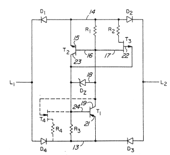
A discrete component form of the switching circuit is
illustrated in Figures 2 and 3. In those figures, node 13 is more
positive than node 14. A bipolar pnp transistor Tl is connected
to a bipolar npn transistor T2 such that the base of each device
is connected to the collector of the other device. The emitter of
transistor Tl is connected to node 13, and the e~itter of
transistor T2 is connected to node 14. Transistor T2 has a bypass
resistor Rl connected between its emitter and base, and a zener
diode Dz connects the bases of the transistors. Transistor T3 is
a p-channel depletion-mode field-effect transistor (FET) having
its source connected to the base of transistor T2 and its drain
connected through a resistor R2 to node 14. The gate of FET T3 is
connected to the collector of transistor T2. ~nother bypass
resistor R3 (shown in outline in Figure 2) can be connected
between the emitter and base of transistor Tl.
With reference to the forward blocking region denoted in
Figure 1, the voltage differential between nodes 13 and 14 must
exceed the threshold value VBF before the switching circuit of
Figure 2 turns on. Once the circuit turns on, large currents pass
between nodes 13 and 14 through a small differential forward
voltage VF. The discrete component circuit of Figure 2 operates
in the following manner. In the forward blocking state the
negative voltage on node 14 is experienced at the emitter 15 of
transistor T2. Through the forward polarized emitter-base
junction of transistor T2 and resistor Rl this voltage appears at
the base 16 of transistor T2, at the source 17 of FET T3, at the
anode 18 of zener diode Dz, and at the collector 19 of the
transistor Tl. Similarly, the voltage on the positive node 13 is
experienced at the emitter 21 and base 24 of the transistor Tl, at
the cathode of the zener diode Dz, and at the collector 23 of
transistor T2. Transistors Tl and T2 are not conducting and a
large impedance exists between the cathode and the anode of zener
diode D~. The voltage between nodes 13 and 14 appears essentially
unchanged between the drain 17 and gate 2~ of FET T3. As a
result, FET T3 is not conducting and the resistor R2 is
essentially disconnected from the base 16 of transistor T2. Below
the breakdown voltage of zener diode Dz, this circuit is
functioning in the forward blocking region on the voltage-current
characteristic o Figure 1.
Once the voltage differential between nodes 13 and 14
exceeds the breakdown voltage of the zener diode Dz, current
passes through the resistor Rl, through zener diode Dz and through
the emitter-base junction of transistor T1. When this current
reaches a value such that the voltage drop across the resistor R
exceeds the threshold voltage oE the emitter base ~unction of
transistor T2 (approx. 0.6 volts), current begins to pass between
the collector 23 and emitter 15 of transistor T2. Transistors T
and T2 both begin to turn on, and a positive feedback action
results from the connection of the collector 23 of transistor T2
to the base 24 of transistor Tl and the connection of collector 19
of transistor Tl to the base 16 of transistor T2. The onset of
this process is defined by the value of the resistor Rl, and
corresponds to the breakover point VBF2 in Figure 1. The positive
feedback action causes the collector-emitter currents of both of
the transistors T1 and T2 to increase, resulting in eventual
saturation of both transistors; the current increase is reflected
by the line 12 in Figure 1. Simultaneously, the differential
voltage between the collectors 19 and 23 decreases to a low value,
and the voltage differential between nodes 13 and 14
correspondingly decreases to the holding voltage V2 shown in
Figure 1. The device is then in the forward conducting state.
With this invention, as the voltage differential between
the collectors 19 and 23 decreases, the voltage differential
between the gate 22 and source 17 of FET T3 also decreases. FET
T3 is a depletion-mode device, its source-to-drain resistance
2~
varying in inverse prooortion to the voltage differential between
gate 22 and source 17. FET T3 is selected so as to be ~ully
non-conductive when the voltage differential between nodes 13 and
14 is, for example, equal to 90~ of VBo and fully conductive when
the voltage differential between nodes 13 and 14 is approximately
equal to VF. In the conductive state, the resistor R2 is
connected essentially in parallel with the resistor Rl. The
parallel combination of resistors R2 and Rl determines the holding
current IH and the holding voltage VH in the same way that the
resistor Rl determines the latching current IL and the breakover
voltage VBF, as depicted in Figure l. The ratio of the holding
current to the latching current is approximately equal to the
function (Rl/R2)+1.
As illustrated in Figure l, the presence of FET T3
creates a pronounced separation between the latching current and
the holding current. Line 12 represents the switching
characteristic for the circuit of Figure 2, while line 11
represents the switching characteristic for the same circuit with
FET T3 shorted and resistor R2 connected directly to base 16 of
transistor T2. By allowing for a decrease in the latching current
with respect to the holding current, the device provides
independent control of the holding and latching states.
Figure 3 combines the circuit of Figure 2 with a diode
bridge comprised of four diodes, Dl, D2, D3 and D4. The diode
bridge rectifies voltage differentials appearing across Ll and L2,
and results in node 13 always being more positive than node 14.
The FET transistor T4 and resistor R4, which are shown in outline
in Figure 3, may optionally be added to the circuit to increase
the range of control over the ratio o~ holding to latching
currents; those components act in a manner complementary to that
earlier described with respect to FET transistor T3 and resistor
R2 .
Figures 4 and 5 illustrate a second embodiment of the
invention, an implementation of the circuit on a semiconductor
wafer. The wafer has two p-type regions, pl and p2, each
extending on an opposite side of a n-type region, nl. A n-type
region, n2, extends into the p2 region. One means of producing
such a structure is by diffusion of a p-type dopant into a n-type
' , : ' ,
'
22
substrate, with subsequent difEusion of a n-type dopant into one
of the p-type regions created by the first dif-Eusion. Planar
conduction layers 34 and 35 each extend across a respective
opposite side of the deviceO Isolation layers 36 and 37 define
the sides of the pl, p2 and n2 regions. The n2 region is created
with a series of windows 38 through which the p2 region extends to
contact conduction layer 34. Whenever reference is made hereafter
to the width of the p2 region, that reference is to the distance
between the nl and n2 regions and not to the width of the p2
region at the windows 38.
Although the semiconductor device of the second
embodiment of the invention appears quite dissimilar to that of
the first embodiment, their operation is analogous if the
dimensions and doping levels of the semiconductor device are
selected appropriately~ Thyristor devices having a structure
similar to that shown in Figures 4 and 5 are usually designed such
that the width of the p2 region between the nl and n2 ~e~ions is
several times greater than the maximum width of the depletion zone
in the p2 region at the breakdown voltage of the device. In the
second embodiment of the invention, the width and doping level of
the p2 region must be closely controlled. Below the breakover
voltage of the device, current is prevented from passing through
the device by the reverse-bias zone at the junction of the nl and
p2 regions. As the voltage across the device is increased toward
the breakdown voltage, the width of the depletion zone at the
nl-p2 junction increases. A first portion of the depletion zone
extends into the p2 region; it has a width a1. Another portion of
the depletion zone extends into the nl region; it has a width a2.
With the device of this invention the width of the p2 region is
only slightly greater than the width e~pected of the depletion
zone in the p2 region at the breakover voltage of the device. The
excluded portion of the p2 region, ie. that portion which remains
outside of the depletion zone and varies in thickness with the
voltage differential applied to the device, acts in an analogous
manner to the channel of the FET transistor of the discrete
component embodiment. The resistance of the excluded portion of
the p2 region to current flow parallel to the nl-p2 junction
varies with the thickness of the excluded portion, ancl thus varies
with the voltage applied across the device. The nl region may
optionally extend through the pl region to contact the conductor
35 by means of the series of cylindrical windows 39 shown in
outline in Figure 4. That optional structure, which can be made
equivalent to the FET transistor T4 and resistor R4 of Figure 3,
may be added to create a slight improvement in circuit
performance.
The analogy between the first and second embodiments of
the invention has been made clearer by placing symbols for the
analogous discrete components onto the cross~sectional view of the
semiconductor wafer of Figure 5. A npn transistor (T2) is drawn
between the nl, p2 and n2 regions, and a pnp transistor (Tl) is
drawn between the pl, nl and p2 regions. Current entering the
base of the npn transistor moves from conduction layer 34 through
one of the windows 38. After passing through the window, the
current passes through that portion of the p2 region that i5
outside of the depletion zone of the nl-p2 junction; it moves in a
direction parallel to that junction. Alternate FE'r transistor T4
and resistor R4 are shown in outline in Figure 5 for the case
where the windows 39 are present in the pl region.
Figure 6 illustrates a semiconductor wafer in which two
switching devices of the second embodiment of the invention are
present. The devices are positioned back-to-back, and act in a
manner functionally equivalent to a bidirectional diode thyristor.
The pl, nl, p2 and n2 regions form a device having a switching
characteristic corresponding to that previously described (and
illustrated in Figure 1). The n3, pl, nl and n2 regions form a
second device having a switching characteristic which is similar
in shape to that shown in the first quadrant of Figure 1 but
adapted to extend in the third quadrant. Figure 7 illustrates the
switching characteristic for the device of Figure 6.
With respect to the basic form of the invention shown in
Figures 1 to 5, an example will next be given to illustrate the
calculation of the relative width of the n and p regions necessary
to create in a semiconductor wafer voltage-current characteristics
; analogous to those described wi~h respect to the discrete
component version of the switching circuit.
The ratio of the holding current to the latching current
2;2
is first selected; this ratio will be designated 'm'. In the case
of an integrated protection device having a breakover voltage of
300 volts and a holding current equal at least to approximately
0.25 amperes to 0.3 amperes, the preferred value of the latching
current is equal to approximately 30 milliamperes or less~ The
minimum 'm' value is thus approximately 12. Therefore, the ratio
of the sheet resistance of the p2 region hetween the nl and n2
regions in the forward conducting state to the sheet resistance of
that p2 region at the breakover voltage should also be
approximately 12.
The sheet resistance of the p2 region in the forward
conducting state defines the holding current of the device through
the approximate equation:
ih=(Vbeh)/(Rsb) ( )
where ih is the holding current, Vbeh is the potential drop across
the nl-p2 junction at turn-off, Rsb is the sheet resistance of the
p2 region with Vbeh applied, and K is a constant re~erred to as
the 'effective emitter aspect ratio' which depends on the geometry
of the p2 and n2 regions, ie. the amount and relative size of the
p2 and n2 regions. Vbeh is a weak function of current and the
effective emitter aspect ratio. If a value for K of 7000 is
assumed, Rsb at Vbeh must be no greater than 13,000 oh~s. At the
breakover voltage RSb should be at least 155,~00 ohms.
In this example, it is assumed that the p2 region base
layer and the n2 region emitter layer are produced by means of a
two-step diffusion which results in the shape of the distribution
of the doping elements in those layers being approximated by the
normal distribution function. The preferred end doping surface
concentration of the p2 base layer after diffusion is
approximately equal to 101~ cm 3. This value results from the
compromise between the goal of introducing the maximum amount of
the dopant to the base layer without substantially decreasing the
lifetime of the minority carriers in that layer. In this example,
a 4-~m. p2 layer is created by the initial diffusion. To produce
the required breakover voltage, the nl background wafer doping
should be approximately equal to 7X10l4 cm 3. A voltage of 0~6
volts applied across this device will produce a depletion layer
--10--
that penetrates the p2 layer to a depth of approximately 0.45 ~m.,
while a voltage of 300 volts applied across this device will
produce a depletion region that penetrates the p2 layer to a depth
of approximately 1.385 ~m. (2.615 ~m. of the p2 diffusion layer
not being included in the depletion region). In order to produce
the desired holding current and the Im' value the n2 layer
- thickness required is 2.5 ~m. A second diffusion is then
performed in which the n2 emitter layer is created having an end
doping surface concentration approximately equal to 5X1019 cm 3.
This process produces a device in which the p2 net base sheet
resistance under the n2 emitter is equal to approximately 12,910
ohms at 0.6 volts applied to the device, and equal to
approximately 155,000 ohms at 300 volts. For every selected value
of 'm' and specified parameters for the p2 and n2 regions, the
corresponding depth of the n2 region has a unique value.
Although the described embodiment has related to a
device Eormed on a n-type substrate material, a complementary
device could be formed on a p-type substrate material. A first
diffusion process would be utilized to transform opposite sides of
the substrate material into nl and n2 regions, and a subsequent
diffusion process would be utilized to transform an outer portion
o~ the n2 region into a p2 region. In this embodiment, a similar
methodology to that previously described would be applied to
determine the depth of the p2 region.