Note: Descriptions are shown in the official language in which they were submitted.
~5~5
FIELD OF THE INVENTION
This invention generally relates to inspecting
apparatus and method for detecting the presence of flaws in
a moving sheet of material.
BACKGROUND OF THE INVENTION
The optical detection of small defec-ts such as
pinholes in continuously-produced sheets of materials such
as aluminum foil, polymer films or paper is an important
requirement for many materials processing industries.
In some cases, such as in the production of sealed
metallic foils for food containers or in the production of
plastic films for electric-insulation applications, the
product must be guaranteed defect-frée so that a 100~
inspection is required. In other cases, an automated
sampling procedure may be applied to determine the trends in
the average density of pinholes across the product for
statistical quality control and process monitoring
requirements.
Pinholes in insulating materials are sometimes
detected by electric-conductance devices using high-voltage
brushes or sponges in contact with both sides of the sheet
for pinhole detection through the establishment of spark
discharges between the electrodes. Such t~chni.qlles are
often unreliable, low-speed, and subject to wear and erosion
problems. Another approach is by liquid or gaseous leak
testing on the assembled container. This approach is quite
expensive in its implementation and in any case cannot be
used by the sheet-producing company which must guarantee a
pinhole-free sheet product to the container-manufacturing
company.
Optical inspection techniques have been
increasingly used for these applications in the last years.
Optical methods are attractive because they are noncontact
- 1 - ~
129~ 5
and thus easy to implement and rapid to scan over large
sheets moving at high speed. A typical known apparatus for
the optical detection of relatively large pinholes comprises
a video camera used to image the moving sheet which is to be
inspected. Backside flash illumination may be used to
localize the pinhole position in fast-moving sheets with
good spatial resolution. The camera may alternatively be
situated on the same side as the illumination source to
detect defects which do not correspond to a perforation of
the sheet.
This known approach is mainly useful for the
detection of relatively large pinholes, of the order of
1 mm in size. For the detection of very small pinholes, of
the order of lO,um in diameter, the camera must be equipped
with a close-up lens of the microscope kind. Such
objectives have a typical operating distance of a few mm and
a numerical aperture (N.A.) of the order of 0.5 to resolve a
pinhole diameter d of the order of 10 ,um. This leads to a
reduced field of view of less than 1 cm2 and to a depth of
field of the order of d/NA ~ 20 ,um, hardly compatible with
typical industrial requirements where a 1 meter-wide sheet
is being drawn at speeds of 10 m/s with transverse
fluctuations of several mm of amplitude.
Another known technique includes the reduction of
the spatial resolution requirements to extend the field oE
view and the depth of field. A standard camera objective is
used to image an area of typically 1 m2 with a 1 mm spatial
resolution. This results in a depth of field of several cm,
relaxing positioning requirements. However, defects smaller
than 1 mm in size often escape detection unless a very
strong illumination power is used to compensate for the low
pinhole/pixel surface ratio.
Still another known technique includes spatial
filtering under continuous illumination. A high-power
~S3~
continuous source is used for backside illumination of the
moving sheet. The pinhole imaged during the camera
integration time of 1/30 of a second will appear as a short
line in the camera image. A sheet moving at 10 m/s will
displace through 0.3 m during the camera integration time.
Knowing the direction of the sheet movement, the camera
image may be digitally filtered to enhance the visibility of
lines oriented along such a direction. Again, spatial
resolution considerations make this approach not sensitive
to very small defects.
Concerning optical reflective techniques, there
are two basic methods for reflective optical inspection
systems: camera viewing under incoherent illumination,
(using lamps, as in U.S. Patent 4,162,126), or laser
scanning (most often with rotating mirrors such as in U.S.
Patent 4,632,S46). Incoherent illumination avoids speckle
but it is affected by a number of problems including reduced
illumination power density, limited depth of field, as well
as long scanning time and difficulty to keep a convenient
air purge over a large window aperture when a two-
dimensional matrix-array camera is used. Laser scanning
offers high instantaneous power, strong immunity to ambient
light, long depth of field and convenient air purging
through a slit, but it requires a delicate mechan:ical
scanning device subject to :Long-terrrl wear, lt is subject to
speckle noise, and requires a very high speed detector to
resolve each pixel during a line scan.
It is an object of the present invention to
provide apparatus and method for detecting the presence of
flaws smaller than the flaws detected with known apparatuses
and methods.
SUMMARY OF THE INVENTION
According to the present invention, there is
lZ95395
provided an apparatus for detecting the presence of flaws in
a moving sheet of material, comprising:
a light source for projecting a light beam;
beam shaping means for shaping said light beam
into a predetermined structured light pattern, and
projecting said strutured light pattern onto a
portion of the surface of said sheet;
optical means for collecting light emitted from
said portion of said surface;
light detecting means for receiving said light
collected by said optical means, and generating an
electrical signal indicative of the intensity of
said light emitted from said portion of sai.d
surface;
signal processing means for filtering said
electrical signal, said signal processing means
having predetermined characteristics specifically
adapted to match an expected electrical signal
corresponding to said predetermined structured
light pattern; and
signal detecting means connected to the output of
said signal processing means for detecting the
presence of flaws in said sheet.
According to the present :invent:i.orl, there is ~lso
provided a method for detect:ing the pr~s~nce of flAws in a
moving sheet of material, comprisirlg the steps of:
a) projecting a light beam;
b) shap:ing said light beam into a predetermined
structured light pattern;
c) projecting said predetermined light pattern
onto a portion oE the surface of said sheet;
d) collecting light emitted from said portion of
said surface;
e) generating an electrical signal indicative of
12i~S3~
the intensity of said light collected during said
step d);
f) filtering said electrical signal with a filter
having predetermined characteristics specifically
adapted to match an expected electrical signal
corresponding to said predetermined structured
light pattern; and
g) detectiny the presence of flaws in said sheet
from the output signal of said filter.
The objects, advantages and other features of the
present invention will become more apparent upon reading of
the following non restrictive description of preferred
embodiments thereof, given for the purpose of examplifica-
tion only with reference to the accompanying drawings.
BRIEF DESCRIPTION OF T~IE DRAWINGS
Figure 1 illustrates in a side view an inspecting
apparatus for detecting the presence of a hole in a moving
sheet of material according to the present :invention.
Figure 2 illustrates in a view from above the
apparatus shown in figure 1.
Figure 3 illustrates in a side view a device that
can be used in the beam shaping unit according to the
present invention.
Figure ~ illustrates ill a s:ide view a device that
can be used in the beam shaping unit according to the
present invention.
Fiyure 5 shows the intensity distribution of the
signal detected when the device shown in figure 3 is used.
Figure 6 shows the intensity distribution of the
detected signal when the device shown in figure 4 is used.
Figure 7 shows the intensity distribution of
figure 5 with noise.
Figure 8 shows the intensity distribution of
i39~
figure 6 with noise.
Figure 9 shows the intensity distribution of
figure 7 after filtering according to the present invention.
Figure 10 shows the intensity distribution of
figure 8 after filtering according to the present invention.
Figure 11 shows the intensity distribution of
the signal detected after filtering according to the present
invention when the device of figure 3 is used while no hole
is present in the sheet.
Figure 12 shows the intensity distribution of the
signal detected after filtering according to the present
invention when the device of figure 4 is used while no hole
is present in the sheet.
Figure l3 illustrates in a side view another
apparatus for detecting the presence oE a hole in a sheet of
material according to the present invention.
Figure 14 illustrates in a view from above the
apparatus shown in figure 13.
Figure 15 illustrates an elevation of another
apparatus for detecting flaws in a moving sheet of
material according to the present invention.
Figure 16 illustrates in a front view the mask
that is used in the apparatus shown in figure 15.
Figure 17 is a transverse section along l:ine 17-
17' of figure 16.
DETAILED DESCRIPT]:ON OE' TIIE D~AWINGS
Referring now to figures 1 and 2, there is shownan apparatus for detecting the presence of a defect 2 in a
moving sheet 4 of material. I'he apparatus comprises a
coherent light source 6 for projecting a light beam. The
light beam is shaped by a beam shaping unit ~ into a
predetermined structured light pattern. The structured
light pattern is projected onto a portion of the surface of
-- 6 --
12~53~
the sheet 4. The apparatus also comprises an optical unit
10 for collecting light transmitted through the sheet 4 when
a hole 2 is present in the sheet. A large size detector 12
receives the light collected by the optical unit 10 and
generates an electrical signal indicative of the intensity
of the light transmi.tted through the sheet 4 when a hole 2
is present. Other kinds of detectors can be used, such as a
linear photodiode array with its axis oriented perpendicular
to the direction of motion of the sheet.
The apparatus also comprises a signal processing
circuit 24 including a filter for filtering the electrical
signal generated by the detector 12. The filter has
predetermined characteristics specifically adapted to match
an expected electrical signal corresponding to the prede-
termined structured light pattern. The signal processing
circuit also comprises a signal detector connected to the
output of the filter for detecting the presence of a hole 2
in the sheet 4.
The beam shaping unit 8 comprises a first
cylindrical lens 14 for converging the light beam in a
direction parallel to the direction in which the sheet 4
moves as indicated by the arrow in figure l. The beam
shaping unit 8 also comprises a second cylindrical lens 16
for expanding the light beam in a direction substantially
perpendicular to the direction in which the sheet 4 moves,
and a device 18 for specificaLly shaping the light beam .i.nto
a predetermined structured light pattern.
The optical unit 10 comprises a wide area lens 20
for collecting the light transmitted through the sheet 4
when a hole 2 is present in a direction substantially
perpendicular to the direction in which the sheet 4 moves,
and a cylindrical lens 22 for focusing the transmitted light
onto the large size detector 12.
The projected beam pattern, which has typically a
lZ~395
width of less than one millimeter in the direction parallel
to the sheet movement, is expanded to a width of the order
of one meter in the transverse direction by use of the
second cylindrical lens 16. The full width of a relatively
large sheet may thus be inspected with a single light source
and detector, while the low signal level resulting from such
a wide spread of the light beam is compensated by the
efficient signal-extraction methods according to the present
invention. The diverging beam is collected, when
transmitted through pinholes, by the wide area lens 20. The
wide area lens 20 can be a Fresnel lens which is compact,
light-weight and inexpensive though providing limited image
sharpness. Such a lim:ited focusing power, as well as the
divergence of the transmitted beam introduced by diffraction
through the pinhole, can be accepted in the present
configuration because of the large size of the detector.
Similar considerations show that the depth of field extends
in this case over several cm, making this apparatus easy to
install and relatively insensitive to sheet flutter.
Referring now to figure 3, there is shown a device
that can be used in the beam shaping unit for specifically
shaping the light beam into a predetermined structured
light pattern. The device comprises an opaque member 26
provided with a sLit 28 having its axis oriented parallel to
the plane of the sheet 4, and perpendicularly to the
direction in which the sheet 4 moves.
Referring now to figure 4, there is shown another
device that can be used in the beam shaping unit 8 for
shaping the light beam into a predetermined structured light
pattern. This device comprises a beam splitting device 30
for splitting the light beam into two secondary light beams,
and reflecting surfaces 32 for superposing the two secondary
light beams at an angle so that the structured light
pattern, projected onto the surface oE the sheet, contains
129~39~
interference fringes. Other light patterns can be produced
using appropriate beam-shaping units.
Referring now to figure 5, there is shown the
intensity distribution of the signal detected when the
device shown in figure 3 is used. The vertical axis
indicates the signal level, and the horizontal axis
indicates the time in microseconds. A simple slit, oriented
with its axis parallel to the sheet plane and perpendicular
to the direction of the sheet movement, produces a
characteristic sin x/x light distribution whose half-width
is inversely proportional to the slit width. Similar light
distributions can be obtained without blocking out part of
the signal by using a transparent phase hologram of similar
shape. Once the light pattern is known, the shape of the
signal expected when a pinhole scans such a light pattern
can easily be recognized even in the presence of substantial
reflected-ambient-light or electronic noise.
Referring now to figure 6, there is shown the
intensity distribution of the detected signal when the
device shown in figure 4 is used. The vertical axis
indicates the signal level, and the horizontal axis
indicates the time in microseconds.
Referring now to figures 7 and 8, there are shown
respectively the lntensity distributions of figures 5 and 6
with noise. The vertical axis indicates the signal level,
and the horizonta:L axis indicates the time in microseconds.
A randomly or exponentially distributed, 1 M~lz bandwidth
noise has been added to the signal represented on figures 5
and 6 to produce respectively the signal represented on
figures 7 and 8. The signal is hardly recognizable when the
noise is introduced.
Referring now to figures 9 and lO, there are shown
respectively the intensity distributions of figures 7 and 8
after filtering according to the present invention. The
12~;395
vertical axis indicates the signal level, and the horizontal
axis indicates the time in microseconds. After filtering,
the signal is effectively extracted from the noise as it can
be seen on figures 9 and 10. The filtering consists of a
deconvolution of the signal plus noise traces with the
expected electrical signal.
Referring now to figures 11 and 12, there are
shown respectively the intensity distributions of the
detected signal after filtering according to the present
invention when the device of figures 3 and 4 are used while
no hole is present in the sheet. The vertical axis
indicates the signal level, and the horizontal axis
indicates the time in microseconds. The filtering consists
of a deconvolution of the noise with the expected electrical
signal. It can be seen from figures 9 and 10 in view of
figures 11 and 12 that there is a quite noticeable
difference between the electrical signals after filtering
depending on whether there is or there is not a hole in the
sheet.
Although holes are an important class of defects
to be detected, other kinds of defects, such as a black spot
or a light scattering defect on a transparent glass panel,
can be detected with the same apparatus. In this latter
case the time signal to be detected has the form oE a small
drop of the otherwise constant light intensity level when
the opaque defect intersects the projected light beam.
Referring now to figures 13 and 14, there is shown
another embodiment of the inspecting apparatus for detecting
the presence of a defect 2 in the sheet 4 of material. The
apparatus comprises a linear array 36 of uncoupled laser
diodes oriented in a direction perpendicular to the
direction in which the sheet 4 moves.
The linear array of uncoupled laser diodes can be
the model LP2A manufactured by Laser Diode Products (trade
-- 10 --
~S3~5
mark). This approach has a number of advantages as compared
to a single-laser design, such as higher eye safety for a
given total power. Although single diode lasers of CW power
up to 1 W are available, which would produce a very intense
power density along the projected line thus improving the
detectability of very small pinholes, such powers are not
recommended because of eye safety problems. Laser
intensities higher than 1 mW/cm2, if inadvertently received
into the eye for durations exceeding 1 second, may exceed
the maximum permissible exposure for safety. Eye hazard is
related to the high collimation of a coherent laser beam,
which may be focused into a very small spot on the eye
retina, eventually causing hole burning and localized
blindness. I'he use of an array of uncoupled laser emitters
of relatively low power correspondingly increases the power
density along the projected line while keeping the power
density of each spot image in the retina of the observer at
a safely low level.
The use of a linear array of uncoupled laser
diodes provides spatial averaging of optical imperfec-tions.
Any dust particles, material inhomogeneities or spattered
specks on the optical lenses or windows produce strong
spatial modulations of the coherent laser beam diffracted by
such impurities. With a single laser source, this may
result in local "blind spots" along the projected larllinar
beam where the local light intensity Ealls below the
required threshold power for detection of small-area
pinholes. A multiple laser source produces a spatial
averaging of the incoherently superposed diffraction
patterns resulting in a more evenly dis-tributed projected
line intensity.
The linear array of uncoupled laser diodes
provides also speckle smoothing. Coherent laser radiation
scattered by particles or by an optically rough surface
1;2~539~
produces a highly contrasted speckle pattern. Again, the
superposition of mutually incoherent speckle patterns from
an array of uncoupled diode lasers results in a considerably
smoother light distribution along the projected line. This
aspect is particularly important when inspecting unpolished-
surface sheets in a reflective configuration.
A low power visible light source 38 is provided
for projecting a visible light beam. A dichroic mirror 40
reflects the visible light beam toward the beam shaping unit
8. The light beam is transmitted accross the dichroic
mirror 40.
The low-power visible light source, such as an
array of visible LED's or a lamp-illuminated slit, is
collinearly superposed to the radiation from the multiple
laser source through the dichroic mirror. Such mirror
reflects the visible radiation and transmits the laser
radiation. This is convenient for alignment purposes when
the laser radiation is invisible, as it is usually the case
with diode lasers emitting in the 780 to 830 nm range. A
more subtle advantage of such a configuration will now be
discussed in terms of eye safety. Lasers are classified in
classes of increasing eye hazard in terms of their power and
spectral range. Invisible radiation is considered more
dangerous than visible radiation because oE the possibili.ty
that a nonspecialist attendant rnay directly stare into the
invisible beam without knowing it. If the light beam is
visible, even an untrained observer will have a natural
aversion to staring into an intense beam: he will
instinctively blink and shift away his sight, thus avoiding
long term retina exposure to a focused laser spot.
Thus, a visible laser beam of 0.5 mW requires less
precautions for on-line installation than an invisible laser
beam of lower power, such as a 0.1 mW beam of 800 nm
wavelength. The interest of having a collinear visible-
lZ95395
light beam of low power superposed to the near-infrared main
beam is now clear: the visible light provides the required
aversion to direct staring, while the near-infrared beam is
convenient in terms of power, availability of rugged and
S cheap diode lasers, and silicon-detector sensitivity. As an
example, an array of 0.8 mW, 800 nm laser diodes could be
superposed to a collinear array of 0.01 mW, 600 nm LED's to
obtain a visible double-wavelength beam with total power of
0.81 mW per element.
The beam shaping unit 8 comprises a first
cylindrical lens 14 for converging the light beam in a
direction parallel to the direction in which the sheet 4
moves as indicated by the arrow adjacent to the sheet 4.
The beam shaping unit 8 also comprises a second cylindrical
lens 16 for projecting the light beam in the direction
substantially-~perpendicular to the direction in which the
sheet moves. The device 18 is specifically provided for
shaping the light beam into a predetermined structured light
pattern.
The apparatus also comprises an optical unit 10
including a wide area lens 20 for collecting the light
transmitted through the sheet 4 in a direction substantially
perpendicular to the direction in which the sheet moves. A
cylindrical lens 22 is provided Eor focusing the transmitted
light onto large size detectors 42 and 46. In this
embodiment, the light source 36 projects a light beam having
a given wavelength. A discriminating beam splltter 44 is
provided for splitting the light emitted from the surface of
the sheet into first and second splitted light beams. The
given wavelength being removed from the first splitted light
beam by means of the discriminating beam splitter 44.
The first large area detector 42 receives the
first splitted light beam and generates a first detected
signal. The second large area detector 46 receives the
- 13 -
~;~9~395
second splitted light beam and generates a second detected
signal. A signal processing system 48 subtracts the first
detected signal from the second detected signal to produce
an electrical signal in which the visibility of flaws is
enhanced. Then the electrical signal can be filtered
according to the present invention.
In an alternative embodiment, the light source 36
projects a polarized light beam. The discriminating beam
splitter 44 is provided with a polarized filter so that the
polarized component of the light emitted from the surface is
removed from the first splitted light beam and not from the
second splitted light beam.
Each detector can be a single large-area unit such
as the model C30802 by RCA (trade mark) or a detector array
such as the model LD20-5A by Centronic (trade mark), each
detector receiving either light of different wavelength
and/or of different polarization by the use of a proper
optical discriminator. Examples of such discriminators
would be either dichroic mirrors or polarization-dependent
beam splitters. The difference between the outputs from the
two detectors will only be sensitive to pinhole transmission
of laser light oE the proper wavelength and polarization
while being insensitive to common-mode noise generated by
reflections of wide-spectral-bandwidth and unpo:Larized
ambient light variations.
The apparatus also comprises a first shielding
enclosure 50 for enclosing among other things the light
source 36 and the beam shaping unit 8. The first shielding
enclosure S0 is provided with first 52 and second 54
apertures. The first aperture 52 is sufficiently large for
permitting to the beam shaping unit to project the
structured light pattern onto the sheet 4. A clean gas is
injected into the second aperture 54.
The apparatus also comprises a second shielding
- 14 -
;39~;
enclosure 56 for enclosing among other things the optical
unit 10 and the large area detectors 42 and 46. The second
shielding enclosure 56 is provided with first 58 and second
60 apertures. The first aperture 58 is sufficiently large
for permitting to the optical unit 10 to collect the light
emitted from the surface of the sheet 4. A clean gas is
also injected into the second aperture 60.
The shielding enclosures are added to provide
convenient protection to the optical elements from the
industrial environment which often contains fumes, vapor or
other impurities. A constant air purge flow is injected in
the enclosure producing an output flow through the slit
through which the laminar light is projected on the moving
sheet. A low-speed flow is sufficient to substantially
reduce the requirements for periodic cleaning of the optical
components, as it is well known by specialists in this
field. We wish to point out that the projection of a
laminar light beam is particularly well adapted to air purge
requirements because the area of the output slit through
which air flow must be maintained, typically a few
millimeters wide, is minimized as compared to the inspection
of an incoherently illuminated two-dimensional area.
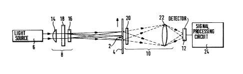
Referring now to figures 15, 16 ancl 17, there is
shown another apparatus for detecting the preserlce of flaws
3 in a moving sheet 4 of material. The apparatus comprises
first 62 and second 64 linear arrays of uncoupled laser
diodes for projecting respectively first and second light
beams. The apparatus includes first 66 and second 68 beam
shaping units for shaping respectively the first and second
light beams into predetermined structured light patterns.
The structured light patterns, formed as laminar light
beams, are projected onto a portion of the surface of the
sheet 4. The two laminar light beams are coplanar. A mask
70 is provided, this mask having an aperture 71 elongated in
- 15 -
12~395
a direction perpendicular to the plane of the laminar light
beams. The apparatus also comprises a camera 72 including a
line array of detecting elements for receiving the light
collected by the mask 70 and generating an electrical signal
indicative of the intensity of the light reflected from the
portion of the surface. The detecting line array and the
first and second linear arrays of uncoupled laser diodes lay
in the plane of ~he laminar light beams.
One of the main noise sources in practical
applications is the presence of ambient light. Unless the
inspected material is perfectly black, ambient light
reflected from the sheet adds to the background noise. As
such noise is generally constant, lt can be largely reduced
by subtractive techniques. The approach that is proposed
consists in using a memory device 74 connected to a signal
processing system 76. The memory device 74 keeps in memory
a continuously updated image of the light distribution
across the sheet as recorded during the last few line scans.
The signal processing system subtracts the newly recorded
image signal from the precedent recorded image signal to
enhance the visibility of the localized image features
corresponding to a pinhole travelling across the field oE
view. Then, the signal processing system ,Eilters the
resulting electrleal signal with a f:ilter having
predetermined characteristics specifically adapted to match
an expected electrical signal corresponding to the
predetermined structured light pattern according to the
present invention.
As it can be seen more speciEically on figure 17,
each beam shaping unit 66 and 68 comprises a cylindrical
lens 14 for converging the light beam in a direction
parallel to the direction in which the sheet 4 moves. Each
beam shaping unit 66 and 68 also comprises a device 18 for
specifically shaping the light beam into a predetermined
- 16 -
3L29~39~
structured light pattern.
This apparatus is also provided with shielding
enclosures 78. Each enclosure is provided with first 80 and
second 82 apertures. The first aperture 80 is sufficiently
large for permitting passage of light. A clean gas is
injected into the second aperture 82 of each enclosure 78.
In this case, both the camera such as the model
1902 by EGG Reticon (trade mark) and the linear array laser
-
sources are situated on the same side of the inspected sheet
which is moving in a direction perpendicular to the plane of
the figure 15. When a surface defect intercepts the
projected laminar beams, it will produce a time-dependent
fluctuation of the signal detected by the detecting elements
correspondi.ng to the position of the defect on the sheet
surface. The use of a multiple-laser array is particularly
important in this case, because different levels of
reflectivity from the light-scattering sheet surface must
here be discriminated, as opposed to a faint transmitted
power over a nominally zero level in the case of figures 1
and 2. Random speckle-related reflectivity fluctuations
must therefore be minimized to avoid false alarms, and the
superposition of a large number of uncorrelated speckle
patterns from an array of uncoupled diode lasers is an
effective method to reduce such Eluctuations.
Another important point which is illustrated in
figure lS is the insertion of a rectangular mask in Eront of
the camera lens, to reduce the lens aperture in a direction
parallel to the direction of the projected line on the
sheet, but to extend as much as possible the aperture in the
perpendicular direction. This increases the depth of field
for the resolution of light fluctuations in the direction of
the projected line axis while keeping the total aperture
surface as large as possible for maximum light collection
and for the minimization of the average speckle grain size
1~9~395
and thus of the speckle noise. Spatial resolution in the
direction perpendicular to the direction of the projected
line on the sheet is assured even if the sheet wobbles out
of focus because of the narrow width of the projected
laminar beams.
The embodiment illustrated in figure 15 does not
require any moving scanner, is moderately affected by
speckle noise, allows each detector element to integrate the
collected light intensity during a relatively long period,
of the order of the line scanning time, so that the required
detector speed is modest, and assures better eye safety than
a single high power scanning laser. As compared to the
incoherent illumination and video imaging approach discussed
in the beginning of the present disclosure, the present
configuration offers monochromatic laser light from which
ambient light can easily be separated by optical filtering,
long depth of field because of the small angular aperture of
the projected laminar beam, strong laser illumination, one-
dimensional scanning much faster than the readout of a two-
dimensional matrix-array camera, and higher transverse
resolution with a standard 2048 element line array as
compared to a typically 480 x 550 element camera.
Although the present invention has been explained
hereinabove by way of preferred embodiments thereoE, it
Z5 should be pointed out that any moclificat:ions to these
preferred embodiments, within the scope of the appended
claims are not deemed to change or alter the nature or scope
of the present invention.
- 18 -