Note: Descriptions are shown in the official language in which they were submitted.
-l- RCA 82,985
SUPER-LUMINESCENT DIODE
The government has rights in this invention
pursuant to a government contract.
The invention relates to a super-luminescent
diode having a radiation confining region whose axis of
symmetry is nonperpendicular to one of the diode's end
faces.
BACKGROUND OF THE INVENTION
High power radiation emitting devices, such
as semiconductor lasers, typically comprise a body of
semiconductor material having opposed end faces in which an
active layer is positioned between two cladding regions of
opposite conductivity. Gain which is necessary for these
high power devices results from a population inversion which
occurs when applied current is increased. The end faces of
the body form a reagonant cavity such that radiation generated
in the active layer is partially reflected back into the
semiconductor body by an end face toward the opposing end
face. When the current is sufficiently increased above
some threshhold value the increase in gain causes lasing
action to occur. Lasers emit a narrow band of highly
coherent radiation having a coherence length of approximately
2 centimeters(cm). Coherent radiation, or radiation
having a high spectral modulation, is undesirable in some
applications, such as fiber optic gyroscopes, which require
high power devices which emit radiation having low coherence.
Other devices such as light emitting diodes (LED's) emit a
broad band of radiation but operate at low power, insufficient
for high power applications.
Super-luminescent diodes (SLDs) provide a high
power output of broad band low coherent radiation, that
being radiation having a coherence length of less than
about 200 micrometers (~m~ and typically about 50 ~m. An
SLD typically has a structure similar to that of a laser,
-2- RCA 82,985
with lasing being prevented by antireflection coatings
formed on the end faces. These coatings must reduce the
reflectivity of the end faces to about 10 5 or less to
prevent lasing in a high power SLD and further, this
reflectivity must be reduced to about 10 6 or less to
achieve low spectral modulation. Spectral modulation is
the percentage ratio of the difference between the maximum
and minimum power output divided by the sum of the maximum
and minimum power output and low spectral modulation is 5%
or less modulation. Unfortunately, low reflectivity of
about 10 6 at the end faces is difficult to obtain
consistently for a given output wavelength and even a
slight temperature change which alters the output wavelength
will change the reflectivity, thus making the manufacture
of a low spectral modulation SLD extremely difficult.
Other SLD structures utilize a stripe interrupt
geometry in which a metallized stripe is formed over a
portion of an active region. This stripe extends from
one end face towards but not up to the opposing end face.
During device operation of these SLDs a reflecting interface
is formed under the end of the metallized stripe which does
not extend to the opposing end face due to differences in
propagation characteristics in the active region, where
current is not supplied by the metallized stripe. This
interface results in high spectral modulation even at
moderate power levels.
Due to the aforementioned problems, an SLD
has been limited to a maximum output power of about 7 mw
continuous wave (cw) and has had high spectral modulation,
typically 50% at maximum power and 20% at half power.
Thus, it would be desirable to have an alternative
construction for SLDs and method for making same.
S~MMAl~Y OF '1'~; INVENTION
~.
A low coherence light-emitting device co~prises a
body having a pair of end faces and an optical path extending
Q~
-3- RCA 82,985
between the end faces. The optical path has an axis of
symmetry and at least one of the end faces is inclined at
an angle relative to a plane perpendicular to the optical
axis. The tangent of this angle is greater than or equal
to the width of the optical beam path divided by the length
of the body between the end faces.
The invention also includes a method of making
the low coherence device by forming at least one of the end
faces such that the end face is inclined at an angle relative
to a plane perpendicular to the optical axis. The tangent
of the angle is greater than or equal to the width of the
optical path divided by the length of the body between the
end faces.
BRIEF DESCRIPTION OF THE DRAWING
FIGURES 1 and 3 are perspective views of different
embodiments of a light-emitting device of the invention.
FIGURE 2 is a top view of the light-emitting device
of FIGURE 1.
FIGURE 4 is a top view of an optical system for
coupling radiation from the light-emitting device of the
present invention into an optical fiber.
P~SC ~
DETAILED D~-~CnITrIO~ OF PREFERRED EMBODIMENTS
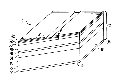
As shown in FIG. 1, a light-emitting device 10
comprises a body 12 having first and second opposed end
faces 13 and 14, respectively, and sidewalls 16 extending
therebetween. As shown in FIGURE 2, the body contains an
optical path 18 having an optical axis of symmetry. At
least one of the opposed end faces 13 and 14, respectively
is inclined at an angle ~ relative to the plane perpendicular
to the optical axis. The body 12 includes a substrate 22
having a first cladding layer 24 thereon, an active layer
26 overlying the first cladding layer 24, a second cladding
layer 28 overlying the active layer 26, and a capping layer
-4- RCA 82,985
30 overlying ~he second cladding layer 28. An electrically
insulating layer 32, having an aperture 34 therethrough,
extends between the end faces 13 and 14, respectively, and
overlies the capping layer 30. A means for electrically
contacting the body 12 comprises a first electrical contact
40 which overlies the surface of the substrate 22 opposite
the first cladding layer 24 and a second electrical contact
42 which overlies the capping layer 30 in the aperture 34.
The tangent of the angle ~ must be greater than
or equal to the effective width of the optical path 18 in
the device divided by the length of the body between the
end faces 13 and 14, respectively. This minimizes the
Fabry-Perot reflections which occur in a laser cavity due
to the reflections occurring between the end faces 13 and
lS 14, respectively.
The width of the effective optical beam path 18
is typically determined by obtaining an intensity beam
profile by attaching a camera and a linear array of
detectors to a microscope. The camera provides a direct
view of the emitting facet and the output of the detectors
provides an intensity beam profile. Alternatively, a
vidicon camera in which a charge density pattern is formed
on a photoconductor may be scanned with an electron beam
in a single line to obtain the intensity beam profile.
Typically, the beam width is determined by the half width
of the beam profile. Alternatively, the 2a or 3~ widths
of the profile may be used to further reduce any possible
feedback.
The angle2~ must also exceed the critical angle
~c for reflections which occur at the boundary of the
optical path. For example, as shown in FIG. 1, the fulcrum
of the angle ~ may extend in the transverse direction, that
being the direction perpendicular to the plane of the layers.
Therefore, when radiation generated in the device 10 travels
along the optical path 18, the light which is reflected by
. the end face will travel in a direction which has components
in both the direction parallel to the optical axis and the
lateral direction, that being the direction perpendicular
_5_ RCA 82,9~5
to the sidewalls 16. Therefore, the reflected radiation
will travel in the plane of the layers and will be absorbed
by the active layer 26 outside the optical path 18. However,
the active layer 26 has differences in its effective
refractive index between that portion of the active layer
26 containing the optical path 18 and the remaining portion
of the active layer 26. These differences in refractive
index serve as boundaries which confine radiation within
the optical beam path of the device, providing total internal
reflection and thereby resulting in high spectra~ modulation.
Therefore, the angle 2e must ~e greater than the critical
angle to prevent reflections in the optical path at these
boundaries. The critical angle eC is determined as follows:
ec = sin~l [1-(n2/n1)2]~
where nl is the effective refractive index of the active
layer 26 containing the optical beam and is typically about
3.355 for AlGaAs and n2 is the effective refractive index
of the remaining portion of the active layer and is
typically about 3.35 for AlGaAs. Therefore, ec is
typically about 3.13 and the angle 2e must be greater than
3.13 and is chosen to be about 5O to account for
diffraction spread. The angle e may be about equal to the
Brewster angle which is egual to the inverse tangent of the
refractive index of the medium adjacent the first end face
13, ~ivided by the transverse effective refractive index
for light propagating between the end faces 13 and 14,
respectively. The medium adjacent the first end face 13 is
typically air having a refractive index of about 1 and the
refractive index of the body 12 is typically 3.35 for GaAs
- devices. Thus, the Brewster angle is typically about 16.6.
At the Brewster angle the radiation vibrating in the plane
of incidence is not reflected, thus resulting in radiation
which is predominantly polarized. Further, at this angle
the reflected and refracted rays are 90 apart resulting in
a non-reflective condition at the emitting end face. This
condition allows the elimination of antireflection coatings
~'
-6- RCA 82,985
on ~he device's end faces which are typically used to
increase output.
It should be understood that the fulcrum of the
angle ~ may extend in other directions, such as the lateral
direction, as shown in FIG. 3. Accordingly, the radiation
reflected from the inclined facet will travel in a direction
whose components are in both the direction parallel to the
optical axis and the transverse direction. Therefore, the
reflected radiation will be absorbed by the first and second
cladding layers 24 and 28, respectively, which typically
have an effective refractive index of about 3.25. Since
the effective refractive index of the active layer is about
3.35 for AlGaAs, ~c is typically about 14. It should be
understood that the differences in effective refractive
index between the layers may necessitate that ~c be greater
than the critical angle of the interface between the
emitting end face of the device 10 and the medium adjacent
the emitting end face. ~owever, if this angle is exceeded,
the radiation will not be emitted from the emitting end
face and will undergo total internal reflection.
m e end face which is inclined may be either
the first or second end face 13 and 14, respectively.
Preferably, the emitting end face is inclined and the
non-emitting end face is perpendicular to the optical axis
and has a lens with a reflective coating thereon positioned
adjacent the non-emitting end face to provide a means for
redirecting a portion of the radiation back into the device
such as disclosed by Gerard A. Alphonse in Canadian
application Serial No. 561,105 filed March 10, 1988
entitled "Low Coherence Optical System Having Reflective
Means." This embodiment will provide greatly increased
radiation from the emitting end face since the device 10
may be modeled as an amplifier in which the output is
related to an exponential function of the length of the
optical path 18 and a function of the current density in
the device 10. Thus, the reflected radiation from the
non-emitting end face when redirected into the active layer
'~` 26, will be reamplified exponentially resulting in
increased radiation from the emitting end face.
-7- RCA 82,985
The substrate 22, first cladding layer 24, and
capping layer 30 are of one conductivity type and the
second cladding layer 28 is of the opposite conductivity
type. The refractive index of the active layer 26 is
typically greater than the refractive index of both the
first and second cladding layers 24 and 28, respectively.
The body is typically composed of binary group III-V
compounds such as GaAs and alloys of such compounds.
The substrate 22 is typically composed of N-type
GaAs about 100 micrometers (~m) thick and has a first major
surface parallel to or slightly misoriented from the (100)
crystallographic plane. The first cladding layer 24
typically combines the function of a buffer layer and a
cladding layer. The first and second cladding layers 24
and 28 respectively, are about 1.5 ~m thick and are
typically composed of AlxGal xAs where x is generally
between about 0.3 and 0.4 and typically about 0.4. The
active layer 26 is typically about 0.08 ~m thick and is
generally composed of A1xGal xAs where x is between about
0 and 0.1, depending on the wavelength to be emitted.
The capping layer 30 is typically about 0.5 ~m thick and
is typically composed of N-type GaAs with zinc diffused
therethrough in the region of the aperture 34. The
insulating layer 32 is typically about 0.01 ~m thick and is
preferably composed of silicon oxide deposited by pyrolytic
decomposition of a silicon-containing gas, such as silane,
in oxygen or water vapor.
Typically, the emitted radiation has an axis of
symmetry which is inclined at an output angle ~ relative to
the direction parallel to the optical axis of symmetry.
The output angle ~ is determined by:
1 n Sin
~ = Sin 1 n
where n1, is the transverse effective refractive index of
- the device 10 and n2 is the refractive index of the medium
adjacent the first end face. For example, as shown in
FIG. 4, a GaAs device 10 in air having an angle ~ of 16.6
.
-8- RCA 82,985
will emit radiation at an output angle ~ of about 73.3
relative to the longitudinal direction. Optical coupling
from the device 10 to a receiving device such as an optical
fiber 50 may be obtained by inclining the fiber's end face
54 such that it is nonperpendicular relative to the fiber's
axis and radiation propagates along the fiber's axis such
as disclos~d by M. Toda et al. in Cdn. S.N. s62,394 filed
March 24, 1988 entitled ~Optical Coupling System."
The body 12 may be fabricated using liquid-phase
epitaxy techniques to deposit the layers. Suitable liguid-
phase epitaxy techniques have been disclosed by Nelson in
U.S. Patent No. 3,565,702 and Lockwood et al. in U.S. Patent
No. 3,753,801. - -
The first electrical contact 40 is preferably
composed of sequentially deposited germanium, gold, nickel,
and gold layers. The second electrical contact 42 is
preferably composed of titanium, platinum and gold layers
which are sequentially deposited onto a zinc or cadmium
diffused surface.
The end faces are typically inclined by mounting
the device 10 at a desired inclination on a polishing
fixture and subsequently polishing the device until the
desired cut is made. Alternatively, the inclination may be
made by sawing, wire cutting, grinding or ion milling. It
may be desirable to employ chemical etching to avoid stressesbeing created in the device 10. Accordingly, an etchant
may be used whose etching rate is a function of the mole
fraction of the device's composition. A sulfuric acid and
hydrogen peroxide etchant will result in an etching profile
which is a function of the Aluminum mole fraction of the
device. Therefore, since each layer of the device 10 has a
different Aluminum mole fraction, the etching will produce
an angle across the layer.
In the operation of the device 10, a bias voltage
of the proper polarity is applied to the electrical contacts
40 and 42 respectively, producing light emission in the
active region. The inclined end face provides a means for
xeducing on-axis reflections of radiation between the end
faces, resulting in an emission having low coherence.