Note: Descriptions are shown in the official language in which they were submitted.
5426
METHOD FOR 08TAINING ELECTRICAL INTERCONNECT USING A
SOLDERABLE MECHANICAL FASTEN~R
Back~round
The present lnvention ha~ to do with providing an
electrical lnterconnect between the bottom and the top of a
prlnted circuit board (PCB). Such a connection 19 called a
via.
There are various method~ for providing an electrical
connection between the bottom and top Or a PCB in the prior
art. For in~tance, plated througb holes provide an
efrective via; however, thi-~ method Or providing via~ i3
relatively expensive. Similarly the insertion of a wire
~umper through two hole~ in a PCB and soldering the wire to
the board on both the top and bottom sldes is an errective
but expensive method Or providing vla. The wire Jumper
lnsertion method requires hand ~oldering Or the PCB and i~
thererore co~tly and time consuming.
Eyelet~ have been used in the prlor art. For lnstance
metal eyelets may be ~waget lnto a hole ln a PCB.
Sometimes a ¢omponent lead 19 lnserted through the eyelet
berore soldering. For a conventlonal eyelet the top slde
Or the PC8 mu~t be soldered ln a separate operatlon lf a
reliable connectlon through the PCB 19 deslred.
Slmilarly, commercially available "~older-through"
eyelets, that 19 special eyelet~ which utllize capillary
actlon to carry molten solder rrom the bottom slde Or a PCB
to the top slde, allow the solderlng of both ~ides of an
': ~
: , . :
'
~29$~
eyelet in a single operation. Component leads are inserted
through these eyelets before soldering. The eyelet serves
the purpo~e Or strengthenlng the mechanical connection Or
the component to the PCB.
The ma~or drawback Or using eyelet3 ror vias in the
prior art ha3 been the inabllity to provide a reliable
electrical Jolnt. Thermal expanslon due to temperature
cycling orten causea ~oints to crack resultlng in
electrical failure.
SummarY Or the Invention
In accordance with the preferred embodiment of the
present in~ention a method for providing vlas between the
top and bottom of a two-layered printed circuit board (PCB)
is presented. An eyelet extends through a hole in the
PC3. The top Or the PCB ha~ a rlrat conductive layer.
Around the hole the rirst contuctive layer l~ 3haped such
that a conductlve pad ia thermally isolated rrom the rest
Or the rirat conductive layer, except that spokes Or the-
rirst conductive layer extend rrom the conductive pad to
the rest Or the rirst conductive layer. The thermal
iaolation Or the ¢onductive pads alds in heat retention
during 301dering. The eyelet i9 crimped such that crimped
rlngers or tabs Or the eyelet ¢ause the eyelet to be
mechanically retained in the hole. The tabs are curved so
that the tabs do not lie ~lat upon the conductiYe pad. The
bottom Or the PCB is then wave soldered 90 that a base Or
the eyelet is electrically coupled to a second conductlve
`~ 12954'~i
layer on the bottom of the PCB and the tabs are
electrically coupled to the conductive pad on the first
conductive layer.
Various other aspects of this invention are as follows:
A method for providing an electrical connection
between a bottom and a top of a printed circuit board, the
method comprising the steps of:
(a) isolating a first portion of conductive layer on top
of the printed circuit board and around a hole in the
printed circuit board, so that when soldering, heat may be
conserved in the first portion;
(b) inserting an eyelet through the hole:
(c) crimping the eyelet so that tabs of the eyelet
cause the eyelet to be mechanically retained in the hole
and so capillary solder paths to the copper pad are
formed; and
(d) wave soldering the bottom of the printed circuit
board.
A method for providing an electrical connection between
a bottom and a top of a printed circuit board, the method
comprising the steps of:
(a) creating a hole in the printed circuit board;
(b) inserting an eyelet through the hole;
(c) crimping the eyelet so that tabs of the eyelet
cause the eyelet to be mechanically retained in the hole,
so that the tabs are curved and so that the tabs do not lie
flat upon the first portion of the conductive layer; and
(d) wave soldering the bottom of the printed circuit
board.
An electrical connector which provides electrical
coupling between a bottom and a top of a printed circuit
1'~9~26
3a
board, the printed circuit board having a first conductive
layer on top of the printed circuit board, a second
conductive layer on bottom of the printed circuit board and
a hole which extends to the bottom of the printed circuit
board to the top of the printed circuit board, the
electrical connector comprising:
a first portion of the first conductive layer coupled to
the rest of the first conductive layer through a plurality
of conductive spokes, wherein the first~portion surrounds
the hole;
a hollow eyelet having
a middle region positioned substantially within the
hole in the printed circuit board, t~e middle region
having a hollow section extending the~.length of the hole in
the printed circuit board,
a base, coupled to the middle region and extending
out the bottom of the printed circuit board, the base being
shaped in such a way that it does not fit into the hole,
and
a plurality of tabs coupled to the middle region
and extending out the top of the printed circuit board, the
tabs extending from the middle region and curving such that
a first section of each tab extends upward in a direction
out of the hole, a second section of each tab extends in a
direction parallel to the top of the printed circuit board,
and a third section of each tab extends downward toward the
first portion of the first conductive layer; and,
solder placed around the hollow eyelet and the
printed circuit board such that the solder provides an
electro-mechanical connection between the base of the first
hollow eyelet and the second conductive layer of the
printed circuit board, the solder fills the hollow section
of the middle region of the hollow eyelet, the solder
~25~ 6
-3b-
provides an electro-mechanical connection between each of
the tabs and the first portion of the first conductive
layer, and the solder fills regions between the second
section of each tab and the first portion of the first
conductive layer.
Brief Descri~tion of the Drawinqs
Figure 1 shows an eyelet used as a mechanical fastener
in accordance with the preferred embodiment of the present
invention.
Figure 2 shows a portion of a printed circuit board in
accordance with the preferred embodiment of the present
invention.
Figure 3 shows a cross-sectional view of the eyelet
shown in Figure 1, placed in the circuit board shown in
Figure 2.
Figure 4 is another view of the eyelet shown in Figure
1, placed in the circuit board shown in Figure 2.
Figure 5 is a cross-sectional view of the eyelet shown
in Figure 1 after it has been soldered in place in the
circuit board shown in Figure 2.
Description of the Preferred Embodiment
Figure 1 shows an eyelet 10 used to make electrical
connection between the top and the bottom of a printed
circuit board (PCB). Eyelet 10 is a hollow mechanical
fastener made of copper with nickel flash and plated with
tin-lead. Eyelet 10 has been pre-scored, that is, grooves
11 are placed in eyelet 10 for easy separation upon
crimping. Eyelets, such as eyelet 10 are available
commercially, for instance, from Mark Eyelet and Stamping
... .
4 i2~S~26
Inc. 63 Wakelee Road, Wolcot, Connecticut 06716. Diameter
12 Or eyelet 10 l~ 1.52 millimeters. Diameter 13 of eyelet
10 iq 2.41 millimeterq. Len6th 14 Or eyelet 10 i~ 2.87
millimeterq. Length 15 Or eyelet 10 19 2.24 milllmeters.
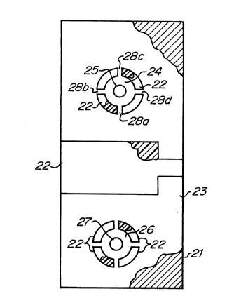
In Figure 2 ls shown a portion Or a printed circuit
board (PC8) 21. PCB 21 should be made out Or material with
a low thermal coerricient Or expansion, e.~., epoxy glass
material. For instance. Norplex, having a place Or
business at 1300 Norplex Drive, La Cross, ~isconsin 64601,
sells a copper clad epoxy base laminate printed circuit
board material which is called CEM 3 tProduct Number
NP525).
Placed on top Or PCB 21 is a copper layer 23. Throu~h
PCB 21 is a hole 25 and a hole 27. Hole 25 and hole 27 are
~or eyelets such a~ eyelet 10. The diameter Or hole 25 and
hole 27 i 1.ô5 mm. Copper }ayer 23 has boen removed ln
portlonJ to eXpOJe an ln~ulatod layer 22. The removal Or
copper layer 23 ha~ lert a copper pad 24 around hole 25 and
a copper pad 26 around hole 27. Out~ide dlameter Or copper
pad 24 and copper pad 26 i9 3.2 mm.
Copper pad 24 and copper pad 26 are coupled to the
remalnder Or copper layer 23 through spokes. For in~tance,
copper pad 24 19 connected to the remainder Or copper layer
23 throu~h a spoke 28a, a spoke 28b~ a spoke 28c and a
spoke 28d. Spokes 28a, 28b, 28c and 28d are part Or copper
layer 23. Each are approximately 0.3 mm wlde and extend a
.
5 1~:9~;~26
distance Or 0.5 mm rrom copper pad 24 to the rest Or copper
layer 23.
Copper pad 24 and copper pad 26 are thermally isolated
rrom the rest Or copper layer 23 ln order to con~erve heat
to the area where eyeletq are soldered.
Figure 3 shows eyelet 10 placed through hole 25 Or PCB
21. Arter bein~ placed through hole 25, eyelet 10 has been
crimped to mechanically rasten eyelet 10 within hole 25.
Tabs 31, 32, 33, 34, 35 and 36 provide mechanlcal and
electrical connection between copper pad 24 and eyelet 10.
Tabs 34, 35 and 36 and copper pad 24 are shown in Figure 4.
Eyelet 10 is not crimped flat, but is rolled. Ir eyelet 10
is crimped too flat, solder will 3tay on tabs 31, 32, 33,
34, 35 and 36, and not ~low onto copper pad 24.
Addltionally, the ahape Or the Jpace between each o~ tabs
31-36 needs to be ~uch as to provide capillary rlow or
~older out onto ¢opper pad 24. Further, eyelet 10 is
crimped to that under itJ own weight~ eyelet 10 is able to
move slightly in and out Or hole 25 without ralling out,
and Jllghtly horizontally, back and ~orth acros~ copper
pad 24. The maxlmum vertical mo~ement and the maximum
horlzontal movement is approximately 0.25 millimeters.
Typically, the crimping iq done ~o that a maximum torque Or
250 ~ram~ per millimeter is required to rotate eyelet 10 ln
hole 25.
Figure 4 ~hows a bird'~ eye view Or eyelet 10 placed
through hole 25. As can be seen tabs 31-36 are shown
6 1295~
makinB meohanioal electrical contact with copper pad 24. A
hole 41 through eyelet 10 allows solder to ~low from the
bottom of PCB 21, over and between tabs 31-36 onto copper
pad 24.
Figure 5 shows a cross-section vlew through the middle
Or hole 25 arter eyelet 10 has been ~oldered lnto place by
solder 51. Wave solderlng i9 used to solder eyelet 10. A
flux that 19 not an organlc acid rlux 19 used ln wave
solderlng ln order to aa~ure that the soldered Jolnt 19
later not subJect to corroslon. The wave soldering i~ done
on the bottom Or PCB 21. Solder masks are used to cover
portions Or the bottom Or PCB 21 which are not to be
soldered. The solder 19 heated to approximately 4?0
deBrees Fahrenhelt. The top Or PCB 21 i9 heated to about
220 degrees Fahrenheit. Solder wave helght should be no
less than one thlrd the thlckneas Or PCB 21 ln order to
insure that ~olter will rlow through hole 41 of eyelet 10,
over and between tabs 31-36 onto ¢opper pad 24. As can be
seen from Figure 5, an area 52 under tab 31 and an area 53
under tab 34 ha~ received ~older, making a well soldered
Jolnt. If the Joint is not well-soldered, as PCB 21 cools
rollowlng the solderlng, thermal contraction Or the
thlckness Or PCB 21 wlll cause the soldered Joint to crack.
.. ..