Note: Descriptions are shown in the official language in which they were submitted.
~$~i7;~
QUASI-RESONANT CURRENT MoDE
STATIC POWER CONVEXSION METHOD AND APPARATUS
.
:::
This invention pertains generally to the field of
static power converters and systems for the control of
static power converters.
BACKGROUND OF THE INVENTION
he d~evelopment and commercial availability of gate
;turn-off devices capable o handling relatively large
;power~levels has~res~lted in a significant :change in power
conver~sion technology. For example,~thyristors are now
rarely u e~ in force-commutated systemsO To a large
extent, the thyri~stor current source inverter has been
replaced by GTO and transistor voltage source inverters at
power ~ratings up to~l me~awatt (MW). The,voltage source
inverter is particularly attractive because of its
15~ extremely simple power structure and the need for only six
uni-directional gate turn-off devices (for three-phase
; load power). The antl-parallel diodes required across
:: ::
:::
35~72
--2--
each of the gate turn-off devices are typically provided
by the manufacturer in the same device packa~e for minimum
lead inductance and ease of assembly. The con-trol
strategy for such voltage source inverters is reasonably
S simple and provides a fully regenerative interface between
the DC source and the AC load.
Despite the clear advantages of the voltage source
inverter structure, the inherent characteristics of
available gate turn-off devices imposes several
limitations on the performance of the inverters. For
example, the high switching losses encountered in such
inverters mandates the u~e of low switching frequencies,
resulting in low amplifier bandwidth and poor load current
waveform fidelity (unwanted harmonics). The rapid change
of voltage with time on the output of the inverter
generates interference due to capacitive coupling. The
parallel diode reverse recovery and snubber interactions
cause high device stresses under regeneration conditions.
In turn, the need to withstand the high device stresses
reduces reliability and requires that the devices be
overspecified. The relatively low switching frequencies
required has also been observed to cause an acoustic noise
problem because the switching frequency harmonics in the
output power!generate noise at audible frequencies in the
switching system and motor. And, in general, present
nverter designs have poor regeneration capability into
the AC supply Line, poor AC input line harmonics,
requiring large DC link and AC side filters, and have poor
fault recovery characteristics.
Ideally, a power converter should have essentially
zero switching losses, a switching frequency greater than
about 18 kHz ~above the audible range), small reactive
components and the ability to transfer power
; ~ bi-directionally. The system should also be insensitive
to second order parameters such as diode recovery times,
device turn-off characteristics and parasitic reactiv~
~ elements. It is clear that present voltage source
::
~g~672
--3--
inverter designs do not achieve such optimum converter
characteristics.
It is apparent that a substantial increase in inverter
switching frequency would be desirable to minimize the
lower order harmonics in pulse width modulated inverters.
Higher switching ~requencies have the aecompanying
advantages of higher current regulator bandwidth, smaller
reactive component size and, or frequencies above 18 kHz,
acoustic noise which is not perceptible to humans.
Increases in pulse width modulated inverter switching
frequencies achieved in the las-t several years (from about
SOO Hz to 2 k~z for supplies rated from l to 25 XW) have
generally been accomplished because of improvements in the
speed and ratings of the newer devices. An alternative
approach is to modify the switching circuit structure to
make best use of the characteristics of available devices.
One well-established approacil is the use of snubber
networks whicll protect the devices by diverting switching
losses away ~rom the device itself. l'he most popular
snubber configuration is a simple circuit strueture in
which a small inductor provides turn-on protection while a
shunt diode and capacitor across the device provide a
polarized turn-of-f snubber. A resistor connected across
the inductor, and diode provides a dissipative snubber
diseharge path. Although the advantages of the use of
snubbers in transistor inverters are well~known, paekaging
problems and the cost of the additional sn~lbber components
has made their commercial use infre~uent. For GTO
inverters, on the other hand, the snubber is absolutely
essential for deviee protection and is o~ten erueial for
reliable and success~ul inverter design. While snubbers
adequately alleviate deviee switehing losses, the total
switching losses do not change appreeiably when losses in
the snubber are eonsidered, and can actually increase from
the losses experienced in cireuits unproteeted by snubbers
under eertain operating conditions. Thus, the increases
in inverter switehing requency which have been obtained
67~
--4--
with the use of snubbers carry a serious penalty in terms
o~ overall system efficiency.
Another alternative is a resonant mode converter
employing a high frequency resonant circuit in the power
transfer path. Two distinct categories of resonant
inverters can be identified. The first category, of which
induction heating inverters and DC/DC converters are
examples, accomplish control of the power transfer through
a modulation of the inverter swi-tching frequency. For
lQ these ~ircuits, the frequency sensitive impedance of the
resonant tank is the key to obtaininy a variable output.
~hile it is also possible to synthesi~e low frequency AC
waveforms using such fre~uency modulation principles,
complexity of control, the large number of switching
devices required, and the relatively large size of the
resonant components limits the applications for such
circuit structures.
The second type of resonant converter, sometimes
referred to as a high frequency link converter, typically
uses naturally commutated converters and cycloconverters
with a high frequency AC link formed of a resonant LC tank
circuit. The high frequency link converters are capable
of AC/AC or DC/AC conversion with bi-directional power
flow and adjustability of tl~e power factor presented to
the AC supply. In contrast to the frequency modulation
scheme of the first category of converters, the link
freque~cy is not particularly important and output AC
waveform synthesis~is done throl~h modulation of the
output stage. For naturally commutated switching devices,
3Q phase angle control is ordinarily used. The high
frequency link converter is generalIy capable of switching
at frequencies greater than 18 kHz using available devices
at the multi-kilowatt power level. However, the
technology has not been economically competitive and has
not been widely used industrially for variable speed drive
type applications. This may be attributed to several
factors. In particular, the large number of
56~
--5--
bi-directional high speed, high power switches required
must be realized using available uni-directional devices.
For example, as many as thirty-six thyristors may be
required in addition to an excitation inverter in some
configurations. The recovery characteristics of the
devices used often necessitate the addition of snubber
networks, lowering the efficiency of the overall system.
In addition, the LC resonant circuit handles the full load
power which is transferred from input to output and has
large circulating cuxrents, e.g., oEten up to six times
the load current. Consequently, even though the total
energy stored in the system is small, the volt-ampere
rating of the resonant elements i~ quite high.
Furthermore, control of such systems is extremely complex
given the simultaneous tasks of input and output control,
high frequency bus regulation, and thyristor commutation
for circuits employing naturally commutated thyristors.
These conventional approaches to voltage source
inverter design assume an a priori relationship between
the inverter losses and the inverter switching frequency.
Most of these commercial designs utilize gate turn-off
devices and operate in the 1 to 2.5 ICHz frequency range
for power levels between 1 and 50 kilowatts. For
commerciall~ available devices, turn-on and turn-off tim~s
of 1 to 2 microseconds are readily available, as are
orage times of 5;to 15 microseconds, enabling these
devices to switch at higher frequencies than used in
conventional designs~. Although the exact switching
frequency is a trade off between system performance and
efflciency, commercially available designs tend to be
thermally limited. In a typical design, approximately 30
to 50% of the total device losses derive from switching
losses. Thus, inverter designs which reduce or eliminate
35~ ~ s~witching losses can yield several benefits. By
decoupling the inverter losses from the switching
~frequency, better device utilization is permitted. Both
the inverter switching frequency and the r~m.s. current
:
:
~9567;~
.
rating can be substantially increased befoxe thermal
limitations occur. Tlle resonant converters described
above can operate with lower ~witching losses but have not
been widely utilized ~or the reasons discussed.
A resonant DC linX inverter design has been developed
which overcomes the most serious objectio~s to the
conventional resonant converters. This design is
disclosed i~ U.S. patent No. 4,730,242 issued March 8, 1988
to the present applicant and entitled
la Static Power Conversion Method and Apparatus Having
Essentially Zero Switching Los~es. An LC resonant tank
circuit i5 excited in such a way a~ to set up periodic
oscillations on the inverter DC link. Under appropriate
control, the DC link voltage can be made to go to zero for
a controlled period of time during each cycle. During the
the time that the DC link voltage goes to zero, the
devices across the DC link can be turned on and of~ in a
lossless manner. By eliminating device switching losses,
the inverter switching frequencies can be raised to above
20 KHz at power ratings of 1 to 25 KW using commercially
availible switching devices such as darlington bipolar
junction transistors. Inverter operation is also
compatible with uniformly sampled zero hystereis bang-bang
controllers~ referred to as delta modulators. When
operated with delta modulation strategies, resonant lin~
converters are capable of better perPormance than hard
; switched pulse width;modulated voltage source inverters.
The resonant DC link inverter also has a simple power
structure and non-catastrophic fault mode which makes the
inverter both rugged and reliable. The major limitation
o the resonant DC link inverter is the imposition of
device voltage stresses of 2.5 to 3 times the DC supply
voltage. A discrete pulse modulation strategy ~or such
resonant link inverters, such as sigma delta modulation,
can also yield su~stantial spectral energy at ~requencies
much lower than the resonant link Prequency. The device
stresses in ~u~h resonant DC linX inverters can be reduced
'
:L~9~
--7--
using clamping of the DC link voltages. The present
lnvention provides an alternate circuit design to that
disclosed, for example, in the aforesaid U.S. patent,
which also realizes high level power conversion with
essentially zero switching losses.
SUMMARY OF THE INVENTION
In accordance with the present invention, DC to AC and
AC to AC power conversion is accomplished with
substantially zero switching losses at switching
requencies to 20 kilohertz and above over a wide range of
power ratings. Current and voltage stresses imposed on
the switching devices are moderate and substantial
improvements are obtained in the spectral response
obtained at the inverter outputs compared to conventional
commercially available inverters. The apparatus cf the
invention operate~ in a quasi-resonant manner, utilizing
an inductor-capacitor resonant circuit, with the directly
; controlled parameter being the inductor current, thereby
operating as a current mode inverter. The ~uasi-resonant
current mode,inverter combines clamped voltage stresses on
the switching devices with the availability of true pulse
~width modulation and sinusoidal output voltages.
In~the inverter apparatus of the invention, an
; : : ad~itional filter capacitor is connected in series with
the inductor of the resonant circuit, the filter capacitor
;having a capacitance~which is substantially greater than
the capacitance of the resonant capacitor so that the
resonan~t frequ:ency will be determined primarily by the
resonant circuit capacitor and inductor. The output power
rom: the inverter is;ta~en across the filter capacitor,
; which filters out the high frequency switching components,
leaving only an AC component, at a much lower frequency
than the switching frequency, which has a substantially
:: ~:::~ :: :
~ ~ '
~ : :
.:
~2~5i6~Z `-
sinusoidal wave shape. A switching means is supplied with
DC power and includes at least a pair of switching devices
which are connected together at a node and to which the
resonant circuit inductor and capacitor are also
connected. Preferably, the resonant circuit capacitor is
comprised of two separate capacitorfi with a resonant
circuit capacitor connected across each one of the
switching devices in the pair of switching devices.
For a single phase inverter, the power source may be
composed of two separate voltage sources of substantially
e~ual supply voltage which are connected in seri~s across
the pair of switching devices and which are connected
together at a node, with the resonant inductor and the
filter capacitor connected between the node of the
switching devices and the node of the power sources. When
the switching devices are switched on, the voltage across
the resonant circuit inductor and series connected filter
capacitor is clamped to the voltage of one of the pair of
voltage sourcesO The switch is turned off at a time when
current is flowing in the switch, and not in an
anti-parallel diode connected in parallel with the switch,
and with zero voltage across the switch so that
substantially no switching loss occurs. The current flow
is then transferred to the resonant capacitor. ~ minimu~
inductor current is required at the time of switching to
insure that the resonant circuit resonates to drive the
voltage level back to the opposite clamping voltage, that
is, to the voltage of the other of the two power sources
the pair. When this voltage is reached, the second of
~the switches in the pair (which has zero voltage across it
at this time) can be turned on to clamp the voltage across
the series connected filter capacitor and resonant
inductor at the voltage o~ the second power source. When
a sufficient current is built up in the inductor to insure
that the resonant circuit will resonate sufficiently to
drive the voltage across the resonant circuit back to the
:
?5~
voltage of the first voltage source, the switch can be
turned off and the resonant cycle repeated. For ideal
inductor and capacitor elements, the minimum switching
current in the inductor is chosen to be greater than or
equal to the square root of the product of the voltage of
each power source and the output voltage across the filter
capacitor divided by the square root of the inductance of
the resonant circuit inductor, all divided by the
capacitance of the resonant circuit capacitor. The output
voltage across the filter capacitor will be a relatively
:10 slowly varying sine wave, e.g., a ~ine wave with a
frequency from G0 to 400 Hz, while the voltage across the
series connected induc~or and the filter capacitor, and
the current through the inductor, may vary at a much
higher switching frequency. For example, the current
through the inductor will appear substantially as a
triangular wave at a frequency which may be as much as
20,000 ~z or higher. Preferably, the switching frequency
is relatively high, e.g., in the range of 18,000 Rz to
20,000 H~ or higher, so that the switching frequencies are
above the audible range.
Under steady state operation when a low frequency
voltage is generated across the filter capacitor, the
switching fnequency of the pairs of switching devices and
the duty cycle both vary continuously depending on the
OlltpUt voltages across the filter capacitor and the
~5 minimum and maximum inductor curren~t envelopes which are
selected to generate the desired low requency output
current through the filter capacito~. These minimum and
maximum current envelopes are selected to insure that the
condition for sustained resonance is satisfied and so that
the averaye of the minimum and maximum current envelopes
approximates the desirad low frequency output current
which will be impressed through the filter capacitor and
which will appear as output voltage across the output
terminals of the inverter. The capacitance of the
resonant circ~lit capacitor or capacitors is pre~erably
cbosen so that durlng the switching cycle, as the current
~2~tS6~
--10--
in the switching device which is turning off goes to zero,
a relatively moderate voltage will be developed across
tnat switching device, preferably as low as possible, thus
reducing substantially the switching losses incurred in
that switching device.
The inverter of the present invention can be extended
to provide three phase output power by utilizing three
pairs of switching devices connected in a bridge
configuration, with the node joining each pair of
switching devices being connected to a series connected
resonant inductor and filter capacitor, and with the
filter capacitor of each of the three phases connected
together in either a wye or delta configuration. The
output voltages for each of the three phases are again
taken across the filter capacitors, and the resonant
capacitors are preferably separate capacitors connected
across each of the switching devices in the three pairs of
switching devices.
A bridge configuration may also be utilized for single
; phase output, employing two pairs of switching devices and
a single power supply, and with the resonant circuit and
; filter capacltor connected between the nodes joining the
switching devices in each pair.
By providing AC output voltages in either of the
single phase or three phase configurations, bidirectional
power flow i5 allowed through the inverter and an AC to AC
converter can also be realized by using two current mode
`inverters and operating them back-to-back off of the same
DC bus.
E'urther objects, features and advantages of the
present invention will be apparent from the following
detailed description when taken in conjunction with the
accompanying drawings.
:::
:~ :
~5i67;~ -
BRIEF DESCRIPTION OF THE VRAWINGS
In the drawings:
Fig. 1 is a schematic circuit diagram of a resonant
pole circuit shown for purposes of illustrating the
circuit operation principles of the present invention.
Fig. 2 are graphs of voltage and current waveforms in
the circuit of Fig. 1.
Fig. 3 is a schematic circuit diagram of a single
phase quasi-resonant current mode inverter in accordance
with the present invention.
Fig~ 4 is a schematic circuit diagram of a single
phase quasi-resonant current mode inverter in accordance
with the invention having separate resonant circuit
capacitors for each of the two switching devices.
Fig. 5 is a schematic circuit diagram of a three phase
quasi-resonant current mode inverter in accordance with
the invention.
Fig. 6 are graphs of current and voltage waveEorms for
the inverter of Fig. 3.
Fig. 7 is an illustrative graph showing the mannner in
which a desired inductor current can be synthesized by
specifying minimum and maximum current envelopes for the
inductor current, yielding an average low frequency AC
inductor current.
Fig~ 8 is a bIock diagram showing a controller which
~provides the switching control signals to the switching
~; ~ dsvices of a quasi-resonant current mode inverter circuit
in accordance with the invention.
Fig. 9 is a schematic circuit diagram of an AC to AC
converter in accordance with the present invention which
utllizes two quasi resonant current mode inverters which
interface between two three phase systems.
:: : :
DESCRIPTION OF THE PREFERRED EMBODIMENTS
With reference to the drawin~s, a resonant pole
:~: : :
~: :
6~2
circuit help~ul in explaining the circuit principles of
the present invention is shown in Fig. 1. This circuit
can be used to provide dc to ac power conversion at the
switching frequency and dc to dc power conversion but is
not capable of dc to ac conversion at an output frequency
lower than the switching frequency. The circuit includes
two voltage sources 11 and 12 of essentially identical
voltage level Vs, a pair of switching devices 13 and 14
(illustrated as bipolar transistors with anti-parallel
10 diod~s 15 an~l 16) configured in an inverter pole and a
resonant circuit composed of a parallel inductor 17 and
capacitor 17 connected between the node 17 at which the
two switching devices 13 and 14 are connected together and
the node 20 at which the two voltage sources 11 and 12 are
connected. A load 21 is connected across the resonant
circuit to receive the voltage across the inductor. The
voltage level stresses imposed on the switching devices
are clamped at the voltage Vs of the voltage supplies 11
and 12. In operation, the first switch 13 is turned on
until the current iL in the inductor 17 is positive in
the direction shown and equals a reference value I .
The switch 13 is turned off at this point to transfer the
current in the inductor iL to the capacitor 1~, and the
resonant pole voltage Vm, the voltage between the nodes
18 and 19, reverses to the level of the negative supply
voltage, -Vs, in a resonant manner. By choosing an
appropriate value for capacitance of the capacitor 18, a
zero voltage turn off for the switch 13 can be attained.
When the pole voltage Vm reaches minus Vs~ the diode
3~ 16 in parallel with the switch 14 turns on, whereupon the
the ~witch~14 can be turned on in a lossless manner. With
the switch 14 and/or the anti-parallel diode 16
conducting, the inductor current iL decreases linearly
until it reaches a value -Ip, at which time the switch
14 can be turned off, and the resonant cycle repeated.
Fig. 2 shows graphs illustrating the pole voltage Vm
.
~9~6~
-13-
wave form 23 and the inductor current iL wave form 24.
The frequency of the output voltage Vm which is
delivered to the load 21 will thus be at the switching
frequency of the devices 13 and 14. The load 21 can
comprise a ~ull wave rectifier which delivers DC voltage
to a power consuming load. However, the circuit of Fig. 1
does not provide variable low frequency output voltage to
tne load and thus cannot serve generally as a DC to AC
inverter.
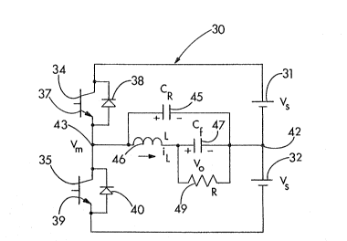
In accordance with the present invention, an inverter
utilizir~g a re~t~nant pole for DC to low frequency P.C
inverter operation is shown generally at 30 in Fig. 3.
l'he inverter 30, which may be designated a quasi-resonant
current mode inverter, includes power supplies 31 and 32
of substantially equal supply voltage Vs, an inverter
pole composed of switching devices 34 and 35 (which as
shown, may be composed, respectively, o~ gate controlled
devices such as the bipolar transistor 37 and
anti-parallel diode 38 and bipolar transistor 39 and
2Q anti-parallel diode 40), with the voltage sources 31 and
32 connected together at a node 42 and the.switching
devices 34 and 35 connected together at a node 43. A
resonant circuit composed of a capacitor 45 and inductor
46 is conneoted in parallel between the nodes 43 and 42
and, in addition, a filter capacitor 47 is connected in
series with the inductor 46 between the nodes 43 and 42.
The output voltage from the inverter is taken across the
filter capacitor 47 and i~ supplied to a load
: illustratively shown as a resistor 49. The phase voltage
Vm between the nodes 43 and 42 is shown by the graph
: labeled Sl in Fig. 6 and the current iL through the
inductor 46 is shown ~y the graph labeled 52 in Fig. 6.
To illustrate the principles of operation of this circuit,
the case may first be considered where it is desired to
generate a DC level output voltage VO across the load
resistance 49. If the positive and negative trip currents
72
-14-
I~ at which switching ta~es place are changed so that
the average inductor current is equal to Vo/R, (where R
is the resistance of the resistor 49) the output voltage
will then be held at VO' It is apparent that this
relationship holds true for all polarities of load voltage
and current, indicatin~ that the circuit 30 can operate as
an inverter. Furthermore, as the directly controlled
parameter is the inductor current, the circuit 30 may be
referred to as a current mode inverter.
The operation of the inverter 30 can be viewed as
composed of two distinct modes, which repeat every half
cycle, with Fig. 6 showing the wave ~orms or the
synthesis of an AC current illustrating the relationships
between phase voltage and inductor current during the two
modes. In the first mode, during which one or the other
of the switches 34 and 39 is turned on, the phase voltage
Vm, which is also the voltaye imposed across the
capacitor 45, is equal to the supply voltage Vs (or
minus Vs). The state equations for the inductor current
iL and output voltage VO are:
~ iL (VS - Vo)/L
O ( L O/ )/C~,
where L is the inductance of the inductor 46, R is the
resistance of the resistor load 49, and Cf is the
capacitance of the filter capacitor 47.
In the second mode, the switches 34 and 35 are turned
off, and the voltage across the resonant capacitor 45 is
no longer clamped to the supply voltage. The state
aquation for the phase voltage Vm is thus
3Q Vm = -iL/Cr, where Cr is the capacitance of the
resonant capacitor 45. ~
The switching conditions are determined based on two
constraints. The first constraint is zaro voltage
switching, which requires that current be flowing in the
switch to be turned off, and that the current be
sufficient to insure that the pole voltage Vm reach the
opposite voltage supply level. ~ssuming that the
i6~2 `--
-15-
capacitance of the filter capacitor is much greater than
the capacitance of the resonant capacitor, by applying
conservation of energy over the first mode, the minimum
value ILmin of inductor current required to reverse the
pole voltaye is:
IL~in = 2 _ ~ VSVO
z
where Z0 = (L/Cr)l/2. This equation assumes
lossless i~ductive and capacitive components. The actual
value o~ ILmin w~uld have to be greater than the value
computed by the equation above to ~mpensate for losses in
the inductive and capacitive components.
A second constraint on system performance is the
variation o~ the switching frequency with the output
voltage V0. Assuming that the transitions between turn
c f of one device and turn on of the other form a small
part of the entire cycle, the inductor current can be
assumed to be substantially triangular in form. Inasmuch
as V0 varies slowly compared to the phase voltage V ,
for purposes of analyzing this constraint the output
voltage can be assumed to be substantially DC. For an
output current Io = Vo/RI the switching period T can
be calculated to be at least (assuming large Z0):
T = 4 ~,z
(V~ - V )
The equation above for T implie.s that for a given load
curr~ent level, as the output voltage VO varies from 0 to
0.8 Vs,~the switching frequency F varies from a maximum,
FmaX, to 0.36 FmaX. If the output voltage increases
to a.s vs~ the switching frequency goes to 0.19 FmaX,
~and if the output voltage VO equals the ~supply voltage
level Vs, zero frequency results. This indicates that
the lowest desirable switching fre~uency sets a limit on
the maximum output voltage (modulation index) obtainable.
:
, ~ ~
:~ :
:; ::
:
~::
~Z5~67;~:
-16-
For a sinusoidally varying output voltage VO~ it can be
seen that the instantaneous switching frequency would
sweep from a maximum value at VO = 0 to a minimum at the
peak voltage point.
A single p'hase quasi resonant current mode inverter
which has a different circuit structure but is otherwise
equivalent to the circuit o~ Fig. 3 is shown generally at
60 in Fig. 4. The circuit 60 has two power sources 61 and
62, each providing output voltage Vs which are connected
together at a node 63, and an inverter pole composed of a
pair of switching devices 64 and 65 which are connected
together at a node 66. In the inverter 60 of Fig. 4, the
switching device 64 is illustratively shown composed of a
~ower MOSFET 68 and anti-parallel diode 69 and the
switching device 65 as a power MOSFET 70 with
anti-parallel diode 71. ~s in the inverter 30 of Fig. 3,
the resonant circuit inductor 73 is connected in series
with a filter capacitor 74 across the phase terminals 66
and 63 and the output voltage VO is provided across the
2Q filter capacitor 74 to a load 75. However, in the circuit
60, the single resonant capacitor 45 of the circuit 30 of
Fig. 3 is split into two substantially equal resonant
capacitors 77 and 78 which are connected across,
respectively,, the switching devices 68 and 70. It is
apparent that the resonant circuit composed of the
resonant capacitors 77 and 78 and the resonant inductor 73
is entirely equivalent to the resonant circuit in the
inverter 30 composed of the resonant capacitor 45 and
~ resonant inductor 46 assuming that the power sources 61
and 62 are ideal and have substantially no internal
impedance. It is seen that t'he capacitor 77 and 78 are
e~fectively connected in paraIlel with one another across
the phase nodes 66 and 63. Thus, if each of the
capacitors 77 and 78 have one half of the capacitance of
the resonant capacitor 45 of Fig. 3, an equivalent
re.~onant frequency is obtained for bot'h of the inverters
~5;6~2 --
-17-
30 and 60, assuming that the inductors 46 and 73 have the
same inductance and that the filter capacitors 47 and 7~
are substantially larger in capacitance than the resonant
capacitor so that the filter capacitors do not
substantially affect the resonant frequency of the
resonant circuit.
A three phase reali7ation of a quasi resonant current
mode inverter is shown generally at 80 in Fig. 5. The
inverter 80 has a pair of power sources 81 and 82 of
voltage level Vs connected together at a node 83 and
three pairs of switching devices 85-90 each composed of a
bipolar transistor and anti-parallel diode, with the three
pairs being connected together at nodes 92-94 in a bridge
configuration. Resonant capacitors 96-101 are connected
across the switching devices 85-90, respectively, and the
three phase nodes 92 94 have resonant inductors 104-106
connected thereto and supply three phase output terminals
107-109 respectively. The output terminals 107-109 have
respective filter capacitors 110-112 connected thereto,
with each of the capacitors 110-112 being connected
together to a common node line 114 which may optionally be
connected by a conducting line 115, shown in dash lines in
Fig. 5, to the node 83 joining the voltage sources 81 and
82. However,, the conducting line llS is not required, and
if eliminated, the filter capacitors 110-112 may be
connected together in either a wye configuration as shown,
or a delta configuration. If the conducting line 115 is
not present, the split voltage sources 81 and 82 may be
combined into a single voltage source. The three phase
circuit of Fig. 5 operates under the same conditions and
~ in the same manner as described above for the circuit of
Fig. 3, with the~three phase currents being individually
monitored to meet the conditions specified above. Of
course, it is also apparent that a full bridge single
phase output may be acheived in accordance with the
~5 present invention utilizing two of the pairs of switching
567~
-18-
devices of Fig. 5 rather than all three. For a single
phase full bridge circuit, the output would be taken
across two terminals, say terminals 107 and 108, in which
case the resonant capacitors 110 and 111 may be combined
into a single equivalent capacitor and the resonant
inductors 104 and 105 ma~ be combined into a single
equivalent inductor.
A further extension of the invention to an AC to AC
converter can be realized by utilizing two current mode
inverters operating back-to-back off of the same DC bus.
Such an AC to AC conversion system is shown generally at
120 in Fig. 9. T'he converter L20 has a three phase output
inverter having switching devices 121-126 connected in
pairs with resonant capacitors 12~-133 connected across
the switching devices. l'he three phase output from the
connections between the pairs of switching devices is
provided to resonant inductors 135-137 and filter
capacitors laO-142 are connected across the three phase
output terminals which are available for connection to a
three phase load-source 143. The inverter receives DC
power from DC bus lines 145 and 146, across which is
connected a large filter capacitor 147 to filter out the
ripples on the DC bus. A rectiEying converter composed o~
switching devices 150-155 is also connected in pairs
across the DC bus lines 14S and 146 and has resonant
capacitors 157-162 connected across the switching
devices. The nodes connecting the two switching devices
in each pair are connected to resonant inductors 165-167
30~ and filter capacitors 168-170 are connected applied to the
three phase input terminaIs which are connected to a three
phase power source 172. The three phase converter
receives the three phase power from the source 172 and
;3 ~ ~ converts it to, DC power across the bus lines 145 and 146.
Reverse directional transfer of energy from the load 143
to the source 172 can be obtained b~ reversing the
fvnctlon of the invereer and converter so that the
~l2~567;2
-19-
inverter composed of the switching devices 121-126
functions to rectify power provided from the load 143 to
DC power on the lines 145 and 146, and the converter
composed of the devices 150-155 can be switched in a
proper fashion to invert the DC power on the bus lines to
AC power which is supplied to the source 172.
The proper control conditions for quasi resonant
current mode inverters in accordance with the present
invention can be further understood with reference to the
single phase circuit of Fig. 3. As noted above, the
capacitance of the filter capacitor 47 is sufficiently
high that this capacitor essentially passes the high
frequency component of the inductor current so that no
substantial high frequency voltage is developed across the
filter ca~acitor. Elowever, the output voltage across the
filter capacitor 47, VO' has a substantial low frequency
content which is the desired output voltage. Preferably,
the capacitance of the filter capacitor 47 is at least an
order of magnitude greater than the capacitance of the
resonant capacitor 45. Such a condition insures that the
high frequency ripple in the output voltage VO is
maintained at reasonably low levels, which is an important
consideration for proper modulation.
Because!the output voltage VO varies at a low
frequency, it can be at a voltage level substantially
different from zero over a large number of switching
cycles. Consequently a net transfer of energy from the
inductor to the filter capacitor 47 is required over each
switching cycle. To generate a low frequency wave form
across the filter capacitor and the load connected in
parallel with it, the inductor current iL must be
controlled such that the low frequency component of
current through the filter capacitor generates the desired
~ output voltage. Thus, the capacitance of the filter
capacitor is chosen so as to filter out the high switching
frequency components bu-t still support the low frequency
: ~:
.
~2~ 2
~20-
component. The modulation strategy controlling the
switching of the switches 34 and 35 must satis~y the
requirement for maintaining the necessary minimum current
iL~in to allow each resonant cycle to continue. ~
maximum current envelope ILmaX, then determines, with
the minimum current envelope, the resulting low frequency
output current I which is desired by the designer. The
minimum and maximum current envelopes and the resulting
low frequency output current wave form I are shown
lo illustratively in Fig. 7. Under steady state operation,
where a low frequency sinusoidal voltage is being
generate~ across the filter capacitor 47, the switching
frequency and the duty cycle will both vary continuously,
as illustrated in Fig. 7, depending on both the desired
output voltage VO and the ILmin and ILmax e p
which are selected. These envelopes are chosen so as to
insure the switching condition given above and to cause
the average of the minimum and maximum envelopes to
approximate the desired output current wave form I .
The value of the resonant capacitor or capacitors is
chosen so that during the switching cycle, as the current
in the device which is turning off goes to zero, a
moderate voltage will be developed across the device
tpreferably as low as possible) to reduce to as great an
extent as possible the switching losses incurred in the
device.
An exemplary controller arrangement for the inverter
of the invention is shown in Fig. 8, wherein the
controller receives as input variables the actual time
varying inductor current IL (received from a current
sensor in series with the inductor 46), the desired low
frequency componet of the inductor current I , and the
actual output voltage VO across the filter capacitor
; (received from a voltage sensor). The value of the output
voltage VO is operated on at 180 to compute a minimum
value of the inductor current required ILmin, which may
;
~5i6~2
-21-
be computed in accordance witll the criterion given above
for the minimum required current level. Depending on the
circuit conditions, the output of the block 180 is a
minimum current ILmin which is selected to insure the
desired maintenance of resonance in the circuit, and the
value of ILmin and the desired low frequency component
I are then utilized as input variables for a
calculation at 181 of ILmaX. This calculation is
carried out so as to yield an ILmaX which results in the
*g ILmax and ILmin being approximately equal
to I The ILmax value is then compared with the
actual inductor current value IL in a comparator 182 to
determine a maximum switching point-and the ILmin value
is compared with the actual current IL in a comparator
183 to determine the minimum switching point. These
values are then used in a conventional fashion to provide
switching inputs to the switching devices 34 and 35.
Preferably, the controller of Fig. 8 is implemented as a
microprocessor based programmable controller which carries
out the calculations shown in the blocks 180 and 181
utilizing software algorithms in a conventional fashion
well known in the art. Although a mircroprocessor system
allowing reprogrammable software to be utilized is
preferred, the blocks 180 and 181 may also be implemented
in a conventional fashion using hard wired circuit
components.
As an example of the implementation of the present
invention, an inverter topology in accordance with the
three phase implementation of Fig. 5 was fabricated and
tested which operated off of a 150 volt DC bus at peak
load currents of 30 amperes. Bipolar switching
transistors with anti-parallel diodes were utilized as the
; switching devices. Each of the resonant inductors had an
inductance of ~0 microhenries, each resonant capacitor had
a capacitance of 0.25 microfarads, and each filter
3S capacitor had a capacitance of 30 microfarads. The
~2~5~7;~: -
-22-
inverter was used as non-interruptable power supply
inverter with sinusoidal output, being switched at
approximately 25 KHz under no load conditions which
reduced to 12 KHz at full load. A pulse width modulation
(PWM) strategy was utilized as discussed above. The value
i~ ILmin was preselected to correspond to the maximum
value of VO to be obtained during normal operation. The
lowest spectral content of the output voltage VO to the
load was approximately 10 KHz, the average switching
losses were less than 10% of the switching losses in a
conventional PWM inverter, the maximum voltage stress
imposed on the switching devices was e~ual to the supply
voltage Vs and the maximum current stress was slightly
more than two times the maximum output current while the
r~m.s. current ratio was approximately 1.2 times the
output current. The output voltage was substantially
sinusoidal.
It is apparent that a wide variety of gate controlled
switching ~evices may be utilized as the switching devices
in the present invention. These include power MOSFETs,
gate turn o~f thyristors, bipolar transistors, and bipolar
darlington transistors, which may be commercially packaged
with anti-parallel diodes or which may include inherent
parasitic anti-parallel diodes.
It is also understood that the invention is not
confined to the partlcular embodiments set forth herein,
but embraces all such ~orms thereof as come within the
scope of the following claims.
: ~
~:
,
:: :
: :
: .