Note: Descriptions are shown in the official language in which they were submitted.
RECONFIGURABLE REGISTER BIT-SLICE ~OR SELF-TEST
Background of the Invention
The present invention relates to testing of
complex logic circuits and, more particularly, to
reconfigurable register bit-slices for use in built-in
logic block observers ~i.e. BILBOs).
Traditionally, large scale integrated circuits
have needed to be tested for defects or flaws. When only a
fraction of the total components produced by a
manufacturing process are ~'goodll (i.e., meet the
requirements of specifications~, something must separate
the "good" components from components which contain defects
or flaws. Testing does this by applying input stimulus
(input test patterns) to the device-under-test and
comparing the outputs of the device-under-test with the
expected llgoodl' results.
In the past, test pattern generation has been
done by hand or with a limited amount of aid from a
computer. As the designs of the circuits being tested
become increasingly complex, the test time required to
generate test patterns by hand increases significantly.
An alternative to expensive manual test pattern
generation exists. Vesigners can incorporate a number of
simple design techniques into their circuit design which
will reduce the cost of test pattern generation and
application while actually allowing better test quality.
In addition, it is possible to build into the circuit to be
. . .
te~ted a number of capabilities typically required of
external test equipment. These built-in self-test (BIST)
techniques can greatly simplify automatic test equipment
requirements and can result in significant costs savings.
Although testability-improvement techniques and
built-in self-test techniques are attractive from the
perspective of test cost reduction, they carry with them
some significant costs which must be evaluated. Most
--2--
design-for-test techniques consume chip real estate, power,
I/O pins and may impact the speed performance of the
circuit during normal operation.
Designs which use built-in self-test provide for
generation of input stimulus and evaluation of the circuit
response within the actual circuit design. To minimize the
on-chip circuitry, external sequencing of the self-$est
operation is often used. A variety of methods exist for
both providing the input stimulus and evaluating the
circuit response. One such method is built-in self-test
with pseudo-random test patterns.
The addition of a test pattern generator, a
parallel signature analysis register, and a serial-scan
register to a logic circuit for testing purposes consumes
chip real estate and power. A solution to the problem of
adding a plurality of test components to a logic circuit
exists which combines the needed functions into a single
register. This register is known as a built-in logic block
observer (i.e. BILBO).
In order to support the various modes of
operation, each BILBO register bit-slice requires front-end
logic which reconfigures the register to a synchronized
set, a serial-scan, a test pattern generator, a signature
analysis or a normal (i.e. parallel load) operational mode.-
Cont~ol inputs of the front-end logic are used to determine
the operational mode of the BILBO.
BILBO registers can be strategically placed
throughout a logic circuit to provide means for testing
sections of the logic circuit. In a typical scenario, a
first BILBO register is configured as a test pattern
generator and a second BILBO register is configured as a
signature analysis register. The test pattern generator
applies a sequence of patterns to a section of a logic
circuit while the results of the test pattern sequence are
compacted by the signature analysis register. When the
test pattern sequence is complete, the second BILBO
register is reconfigured as a serial-scan register and the
compacted results are transferred to another location.
Current designs of BILBO registers comprise a
plurality of bit-slices logically coupled together. The
bit-slices comprise front-end logic which must switch more
than one current switch along a signal path from a data
input to an input of a memory device (e.g. bi-stable
multi-vibrator) while operating in normal mode (i.e.
parallel load). This switching causes a register in normal
operational mode to perform at a slower rate than real-time
speed. Real-time speed, in this instance, is considered
the rate at which a register without front-end logic
operates during the normal operational mode. It is
desirable to utilize front-end logic which has minimal
speed impact upon normal register operation.
The present invention overcomes the problem of
real-time speed operation during normal operation inherent
in previous BILBO register designs. Through clever logic
design techniques, the present invention provides front-end
logic for a BILBO register bit-slice which switches one
current switch along a signal path from a data input to an
input of a memory device (e.g. bi-stable multi-vibrator).
The delay caused by the switching of a one current switch
is equivalent to the delay associated with a 2:1
multiplexer or approximately one gate of delay. Thus, near
real-time speed is obtained during the normal operational
mode because a single current switch occurs along the
signal path.
_4_ ~
64159-1095
Summary of the Invention
A reconfigurable register bit-slice is provided for
use in a BILBO register. More particularly, front-end logic
means is contemplated which switches a single current switch
(e.g. transistor) between a data input means and an output of
the front-end logic means. Thus a single current switch of
delay is added to normal operation of a standard shift register
modified to be reconfigurable.
In accordance with the present invention, there is
provided a register bit-slice, comprising: (a) memory means
for storing a bit, the memory means comprising an input for
receiving a data signal; and (b) front-end logic means,
comprising: (i) an output logically coupled to the input of the
memory means; (ii) control input means for receiving one or more
control input signals; (iii) first data input means for receiv-
ing a first data input signal; (iv) second data input means for
receiving a second data input signal; (v) a current switch;
(vi) means for operating in a first operational mode by
logically coupling the first data input means to the input of
the memory means while switching at most one current switch
along a signal path from the first data input means to the input
of the memory means; (vii) means for operating in a second
operational mode by logically coupling the second data input
means to the input of the memory means; (viii) means for
operating in a third operational mode by providing to the input
of the memory means a logical function generated from the input
signals received from the first and second data input means;
and (ix) means for selectively configuring to one of the
operational modes based on the one or more control input
signals.
In accordance with another aspect of the invention,
there is provided a register bit-slice, comprising: (a) memory
-4a- ~ 0
64159-1095
means for storing a bit, the memory means comprising an input
for receiving a data signal; (b) front-end logic means,
comprising: (i) an output for providing an output signal;
(ii) control input means for receiving one or more control
input signals; ~iii) first data input means for receiving a
first data input signal; (iv) second data input means for
receiving a second data input signal; (v) a current switch;
(vi) means for operating in a first operational mode by
logically coupling the first data input means to the output of
the front-end logic means while switching at most one current
switch along a signal path from the first data input means to
the input of the memory means; (vii) means for operating in a
second operational mode by logically coupling the second data
input means to the output of the front-end logic means; and
(viii) means for operating in a third operational mode by
providing to the output of the front-end logic means a logical
function generated from the input signals received from the
first and second data input means; and (ix) means for
selectively configuring to one of the operational modes based
on the one or more control input signals; and (c) logic level
adjust means for adjusting the output signal provided by the
output of the front-end logic means to a level acceptable to
the input of the memory means, the logic level adjust means
comprising an input for providing a logical coupling to the
output of the front-end logic means and an output for providing
a logical coupling to the input of the memory means.
In accordance with another aspect of the invention,
there is provided a register bit-slice, comprising: (a) memory
means for storing a bit, the memory means comprising an input
for receiving a data signal; (b) front-end logic means, compris-
ing: (i) an output for providing an output signal; (ii) first
control input means for receiving a first control input signal;
~4b- ~;61 10
64159-1095
(iii) seeond control input means for receiving a second control
input signal; ~iv) first data input means for receiving a first
data input signal; (v) second data input means for receiving a
seeond data input signal; (vi) a current switeh; (vii) means
for operating in a first operational mode by logically coupling
the first data input means to the output of the front-end logie
means while switehing at most one current switch along a signal
path from the first data input means to the input of the memory
means when the first control input signal comprises a "true"
signal and the seeond eontrol input signal eomprises a "false"
signal; (viii) means for operating in a second operational mode
by logieally eoupling the second data input means to the output
of the front-end logie means when the first control input signal
eomprises a "false" signal and the seeond eontrol input signal
eomprises a "true" signal; (ix) means for operating in a third
operational mode by providing to the output of the front-end
logie means an XOR logieal funetion generated from the input
signals reeeived from the first and seeond data input means
when the first control input signal eomprises a "false" signal
and the seeond control input signal comprises a "false" signal;
and (x) means for operating in a fourth operational mode
logieally eoupling a "true" signal to the output of the front-
end logie means when the first eontrol input signal eomprises a
"true" signal and the seeond eontrol input signal eomprises a
"true" signal; and (e) logie level adjust means for adjusting
the output signal provided by the output of the front-end logie
means to a level acceptable to the input of the memory means,
the logic level adjust means comprising an input for providing
a logical coupling to the output of the front-end logic means
and an output for providing a logical coupling to the input of
the memory means.
-4c-
64159-1095
Brief Description of the Drawings
Fig. 1 is a logic level diagram showing a BILBO
register utilizing preferred embodiment bit-slices.
Fig. 2 is a logic level diagram showing a preferred
embodiment bit-slice.
Fig. 3 is a transistor level diagram showing a
preferred embodiment front-end logic means utilizing CML design
structures.
Fig. 4 is a transistor level diagram showing a
preferred embodiment front-end logic means and logic level
adjust means utilizing ECL design structures.
Fig. 5 is a transistor level diagram showing a
preferred embodiment bit-slice utilizing CML design structures.
Detailed Description of the Preferred Embodiments
Shown in Fig. 1 is a preferred embodiment BILBO
register 30 comprising serially coupled register bit-slices
2,4,6,8,10,12,14 and 16. The inverted output of a previous
bit-slice is logically coupled to the second data input of the
following bit-slice. For instance, the inverted output of bit-
slice 2 is logically coupled to the serial data input of bit-
slice 4. Each bit-slice further comprises a first data input,
a clock input, an input CTRLl, an input
- --5--
CTRL2 and a second data output. BILBO register 30 operates
in various modes of operation in accordance with the
signals present at CTRLl input and CTRL2 input. BILBO
register 30 further comprises test pattern generation/
S serial scan circuitry 18,20,22 and 24 logically coupled to
the register bit-slices in a manner which enables a serial
scan operational mode or a self-test operational mode
depending upon the signal present at input CTRL3.
Figure 2 shows a logic level description of a
bit-slice used in the preferred embodiments. The
forthcoming logic level description utilizes positive logic
designs. It will be appreciated by those skilled in the
art that a negative logic level description could also be
implemented as an embodiment of the present invention.
Bit-slice 40 can be inserted into bit-slice blocks
2,4,6,8,10,12,14 and 16 in Fig. 1 to provide a full logic
level description of BILBO register 30.
Bit-slice 40 comprises front-end logic means 42
logically coupled to an input of memory means 44. Memory
means 44 preferably comprises means for storing a binary
data bit (e.g., a bi-stable multi-vibrator or a flip-flop),
an output and a clock input. Front-end logic means 42
further preferably comprises a first data input means, a
second~data input means, control input means and logic
means,~ In the preferred embodiments shown, the logic means
comprises OR gate 46 and NOR gate 48 logically coupled to
the inputs of XOR gate 50, and the inputs of OR gate 46 are
logically coupled to the input CTRLl and the first data
input (i.e. DIN). The inputs of NOR gate 48 are
preferably logically coupled to input CTRL2 and the second
data input (i-e- SIN).
Front-end logic means 42 implements a logical
function of the first data input (i.e. DIN), the second
~2~ 10
- --6--
data input (i.e. SIN), input CTRL1 and input CTRL2. In the
preferred embodiment, bit-slice 40 configures to a
plurality of operational modes in accordance with the
output of the logical function provided to the input for
memory means 44. The logical function implemented is
preferably:
(DIN + CTRL1) XOR (SIN + CTRL2~
In the preferred embodiment, the output of this function is
provided to the input of memory means 44. The following
table details the preferred output of the front-end logic
provided to the input of memory means 44.
. . .~
12~
-7-
Table
Node CTRL1 CTRL2 Output of Front-End Loqic
1 1 DIN XOR SIN
3 1 SIN
Bit-slice 40, operating in the first operational
mode, preferably provides the output of [DIN XOR SIN] to
the input of memory means 44. When operating in the second
operational mode, bit-slice 40 preferably provides the
logic signal received by DIN to the input of memory means
44. Further, when operating in the third operational mode,
bit-slice 40 preferably provides the logic signal received
by SIN to the input of memory means 44. Finally, memory
means 44 preferably receives a logical "true" signal when
operating in the fourth operational mode. It will be
appreciated by those skilled in the art that a complement
of the front-end logic output could be provided to the
input of memory means 44. Further, it will be appreciated
by those skilled in the art that other logic functions
could be implemented by the front-end logic to provide
other operational modes.
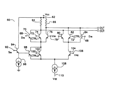
Fig. 3 shows a preferred transistor level
description 60 of the front-end logic 42 of bit-slice 40
shown in Fig. 2. Front-end logic means 60 utilizes
current-mode-logic (CML) design structures. Thus,
typically, Vcc 62 is set to +3.3V and VEE 110 is set to 0V.
Further, VRl 78 is approximately equal to Vcc 62 - ~VBE(on)
- 0.7V and VR2 106 is approximately equal to VRl 78 -
vBE(on)-
When CTRLl 72 and CTRL2 100 are set to a logical
"low" signal, front-end logic 60 operates in the first
operational mode. Thus, transistors 74, 82 and 102 are
~2~?6i1 le)
- --8--
switched off and a logical function of the signals received
by DIN 68 and SIN 92 is provided to outputs 88 and 90. In
the preferred embodiment, the logical function is [DIN XOR
S ]
IN I f the logic signal received by DIN 68 is a
logical "low~' signal with respect to VRl 78, then
transistors 70 and 84 will be switched off and a current
conduction path is provided through transistor 76 or 80.
Further, if the logic signal received by SIN 92 is a
logical ~'low" signal with respect to VR2 106 after having
its voltage level shifted by transistor 94 and current
source 96, then transistor 98 will be switched off and a
current conduction path will be provided through transistor
104. Thus, the current path from Vcc 62 to VEE 110 will be
through resistor 64, transistor 80, transistor 104 and
current source 108. This current path causes a voltage
drop across resistor 64 which results in a logical ~low~
signal being provided to output 90. Because all of the
current from current source 108 passes through resistor 64,
no voltage drop occurs across resistor 66 which results in
a logical ~high~ signal being provided to output 88.
Otherwise, if the logic signal received by SIN 92
is a logical "high" with respect to VR2 106 after having
its voltage level shifted by transistor 94 and current
sour4z~96, then transistor 104 will be switched off and a
current conduction path will be provided through transistor
98. Thus, the current path from Vcc 62 to VEE 110 will be
through resistor 66, transistor 76, transistor 98 and
current source 108. This current path causes a voltage
drop across resistor 66 which results in a logical ~'low~
signal being provided to output 88. Because all of the
current from current source 108 passes through resistor 66,
no voltage drop occurs across resistor 64, which results in
- 9 -
a logical "high" signal being provided to output 90.
If the logic signal received by DIN 68 is a
logical ~high~ signal with respect to VRl 78, then
transistors 76 and 80 will be switched off and a current
conduction path will be provided through transistor 70 or
84. Further, if the signal received by SIN 92 is a logical
"low`' signal with respect to VR2 106 after having its
voltage level shifted by transistor 94 and current source
96, then transistor 98 will be switched off and a current
conduction path will be provided through transistor 104.
Thus, the current conduction path causes a voltage drop
across resistor 66, which results in a logical "low" signal
being provided to output 88. Because all of the current
from current source 108 passes through resistor 66, no
lS voltage drop occurs across resistor 64, which results in a
logical llhigh~ signal being provided to output 90.
If the logic signal received by SIN 92 is a
logical l'high" with respect to VR2 106 after having its
voltage level shifted by transistor 94 and current source
96, then transistor 104 will be switched off and a current
conduction path will be provided through transistor 98.
Thus, the current path from Vcc 62 to VEE 110 will be
through resistor 64, transistor 70 , transistor 98 and
current source 108. This current path causes a voltage
drop-across resistor 64 which results in a logical ~low~
signal being provided to output 90. Because all of the
current from current source 108 passes through resistor 64,
no voltage drop occurs across resistor 66, which results in
a logical llhighll signal being provided to output 88.
When CTRLl 72 is set to a logical "low" signal
and CTRL2 100 is set to a logical "high" signal, front-end
logic 60 operates in the second operational mode. Thus,
transistor 74 and 82 are switched off and a current
~2~
- --10--
conduction path is provided through transistor 102. As a
result, the logic signal received at SIN 92 does not change
the current conduction path because the current is already
flowing through the coupled pair of transistors 98 and 102
and will continue to do so regardless of the logic signal
present at SIN 92. Therefore, a logical function of the
signal received by DIN 68 is provided to outputs 88 and 90.
This logical function is generated by switching a single
transistor (i.e. transistor 70 or 76) along the current
conduction path. Thus, a single transistor (i.e. current
switch) switches along the logical signal path from DIN 68
to output 88 or 90 during the second operational mode.
If the logic signal received by DIN 68 is a
logical ~low~ signal with respect to VRl 78, then
transistors 70 and 84 will be switched off and a current
conduction path will be provided through transistors 76 and
80. Thus, the current conduction path from Vcc 62 to VEE
110 will be through resistor 66, transistor 76, transistor
102 and current source 108. This current path causes a
voltage drop across resistor 66 which results in a logical
"low" signal being provided to output 88. Because all of
the current from current source 108 passes through resistor
66, no voltage drop occurs across resistor 64, which
results in a logical ~high~ signal being provided to output
90.
Otherwise, if the logic signal received by DIN 68
is a logical ~'high~ signal with respect to VRl 78, then
trhnsistors 76 and 80 will be switched off and a current
conduction path will be provided through transistors 70 and
84. Thus, the current conduction path from Vcc 62 to VEE
110 will be through resistor 64, transistor 70, transistor
102 and current source 108. This current path causes a
voltage drop across resistor 64, which results in a logical
-low" signal being provided to output 90. Because all of
the current from current source 108 passes through resistor
64, no voltage drop occurs across resistor 66, which
results in a logical "high" signal being provided to output
88.
When CTRL1 72 is set to a logical ~high~ signal
and CTRL2 100 is set to a logical "low" signal, front-end
logic 60 operates in the third operational mode. Thus,
transistor 102 is switched off, and a current conduction
path is provided through transistor 74 or 82. As a result,
the logic signal received at DIN 68 does not change the
current conduction path because the current is already
flowing through the coupled pairs of transistors 70 and 74
as well as 82 and 84 and will continue to do so regardless
of the logical signal present at DIN 68. Therefore, a
logical function of SIN 92 is provided to outputs 88 and
90 .
If the logic signal received by SIN 92 is a
logical "low" signal with respect to VR2 106 after having
its voltage level shifted by transistor 94 and current
source 96, then transistor 98 will be switched off, and a
current conduction path will be provided through transistor
104. Thust the current conduction path from Vcc 62 to VEE
110 will be through resistor 66, transistor 82, transistor
104 and current source 108. This current path causes a
voltage drop across resistor 66 which results in a logical
"low" signal being provided to output 88. Because all of
the current from current source 108 passes through resistor
66, no voltage drop occurs across resistor 64, which
results in a logical "high" signal being provided to output
90 .
Otherwise, if the logic signal received by SIN 92
is a logical "highl' signal with respect to VR2 106 after
having its voltage level shifted by transistor 94 and
current source 96, then transistor 104 will be switched
off, and a current conduction path will be provided through
transistor 98. Thus, the current conduction path from Vcc
62 to VEE 110 will be through resistor 64, transistor 74,
transistor 98 and current source 108. This current path
causes a voltage drop across resistor 64, which results in
a logical "low" signal being provided to output 90.
Because all of the current from current source 108 passes
through resistor 64, no voltage drop occurs across resistor
66~ which results in a logical "high" signal being provided
to output 88.
Nhen CTRL1 72 and CTRL 100 are set to a logical
"high~', front-end logic 60 operates in the fourth
operational mode. Thus, a current conduction path i3
provided through either transistor 74 or 82 as well as
transistor 102. Therefore, the current conduction path
from Vcc 62 to VEE 110 will be through resistor 64,
transistor 74, transistor 102 and current source 108. This
current path causes a voltage drop across resistor 64,
which results in a logical "low" signal being provided to
output 90. Because all of the current from current source
108 passes through resistor 64, no voltage drop occurs
across resistor 66, which results in a logical "high"
signa~ being provided to output 88.
Fig. 4 shows an alternate preferred transistor
level description 120 of front-end logic 42 of bit-slice 40
shown in Fig. 2. Front-end logic means 120 utilizes
emitter-coupled-logic (ECL) design structures. Thus,
typically Vcc 122 is set to 0 V, and VEE 170 is set to the
negative supply voltage. Further, VRl 138 is approximately
equal to Vcc 122 - ~VBE(on) - 0.7V and VR2 166 is
approximately equal to VRl 138 - VBE(on).
- -13-
When CTRLl 132 and CTRL2 160 are set to a logical
~low~ signal, front-end logic 120 operates in the first
operational mode. Thus, transistors 134, 142 and 162 are
switched off, and a logical function of the logic signals
received by DIN 128 and SIN 152 is provided to outputs 148
and 150 through logic signal level adjust means 146 and
147, respectively. Logic signal level adjust means 146 and
147 adjust the outputs provided by the ECL front-end logic
120 to logic levels acceptable to the input of the memory
means. In the preferred embodiment, the logical function
is [DIN XOR SIN]
If the logic signal received by DIN 128 is a
logical "low" signal with respect to VRl 138, then
15 transistors 130 and 144 will be switched off, and a current
conduction path is provided through transistor 136 or 140.
Further, if the logic signal received by SIN 152 is a
logical ~lowll signal with respect to VR2 166 after having
its voltage level shifted by transistor 154 and current
20 source 156, then transistor 158 will be switched off, and a
current conduction path will be prGvided through transistor
164. Thus, the current path from Vcc 122 to VEE 170 will
be through resistor 124, transistor 140, transistor 164 and
current source 168. This current path causes a voltage
drop across resistor 124, which results in a logical ~lowl'
signaI`being provided to output 150 through logic level
adjust means 147. Because all of the current from current
source 168 passes through resistor 124, no voltage drop
occurs across resistor 126, which results in a logical
"high" signal being provided to output 148 through logic
level adjust means 146.
Otherwise, if the logic signal received by SIN
152 is a logical "high" with respect to VR2 166 after
having its voltage level shifted by transistor 154 and
lZ~
-14-
current source 156, then transistor 164 will be switched
off, and a current conduction path will be provided through
transistor 158. Thus, the current path from Vcc 122 to VEE
170 will be through resistor 126, transistor 136,
transistor 158 and current source 168. This current path
causes a voltage drop across resistor 126, which results in
a logical ~low~ signal being provided to output 148 through
logic level adjust means 146. Because all of the current
from current source 168 passes through resistor 126, no
voltage drop occurs across resistor 124, which results in a
logical "high" signal being provided to output 150 through
logic level ad~ust means 147.
If the logic signal received by DIN 128 is a
logical "high" signal with respect to VRl 138, then
transistors 136 and 140 will be switched off, and a current
conduction path will be provided through transistor 130 or
144. Further, if the signal received by SIN 152 is a
logical "low" signal with respect to VR2 166 after having
its voltage level shifted by transistor 154 and current
source 156, then transi~tor 158 will be switched off, and a
current conduction path will be provided through transistor
164. Thus, the current conduction path causes a voltage
drop across resistor 126, which result~ in a logical "low"
signal~being provided to output 148 through logic level
ad~ust~.means 146. Because all of the current from current
source 168 passes through resistor 126, no voltage drop
occurs across resistor 124, which results in a logical
'Ihigh" signal being provided to output 150 through logic
level adjust means 147.
If the logic signal received by SIN 152 is a
logical "high" with respect to VR2 166 after having its
voltage level shifted by transistor 154 and current source
156, then transistor 164 will be switched off, and a
` f~ ~ l r~
current conduction path will be provided through transistor
158. Thus, the current path from Vcc 122 to VEE 170 will
be through resistor 124, transistor 130, transistor 158 and
current source 168. This current path causes a voltage
drop across resistor 124, which results in a logical ~low~
signal being provided to output 150 through logic level
adjust means 147. Because all of the current from current
source 168 passes through resistor 124, no voltage drop
occurs across resistor 126, which results in a logical
"high~l signal being provided to output 148 through logic
level adjust means 146.
When CTRL1 132 is set to a logical l'lowl' signal
and CTRL2 160 is set to a logical "high~' signal, front-end
logic 120 operates in the second operational mode. Thus,
transistor 134 and 142 are switched off, and a current
conduction path is provided through transistor 162. As a
result, the logic siqnal received at SIN 152 does not
change the current conduction path because the current is
already flowing through the coupled pair of transistors 158
and 162 and will continue to do so regardless of the logic
signal present at SIN 152. Therefore, a logical function
of the logic signal received by DIN 128 is provided to
outputs 148 and 150 through logic signal level adjust means
146 and 147, respectively. This logical function is
generated by switching a single transistor (i.e. transistor
130 or 136) along the current conduction path. Thus, a
single transistor (i.e., current switch) switches along the
logical signal path from ~IN 128 to logic lev~l ad~ust
means 146 or 147 during the second operational mode.
If the logic signal received by DIN 128 is a
logical "low" signal with respect to VR1 138, then
transistor 130 or 144 will be switched off, and a current
conduction path will be provided through transistors 136
P,~
-16-
and 140. Thus, the current conduction path from Vcc 122 to
VEE 170 will be through resistor 126, transistor 136,
transistor 162 and current source 168. This current path
causes a voltage drop across resistor 126, which results in
a logical "low" signal being provided to output 148 through
logic level adjust means 146. Because all of the current
from current source 168 passes through resistor 126, no
voltage drop occurs across resistor 124, which results in a
logical "high" signal being provided to output 150 through
logic level adjust means 147.
Otherwise, if the logic signal received by DIN
128 is a logical "high" signal with respect to VRl 138,
then transistors 136 and 140 will be switched off, and a
current conduction path will be provided through
transistors 130 and 144. Thus, the current conduction path
from Vcc 122 to VEE 170 will be through resistor 124,
transistor 130, transistor 162 and current source 168.
This current path causes a voltage drop across resistor
124, which results in a logical "lowl' signal being provided
to output 150 through logic level adjust means 147.
Because all of the current from current source 168 passes
through resistor 124, no voltage drop occurs across
resistor 126, which results in a logical "high" signal
being provided to output 148 through logic level adjust
means= 146.
When CTRL1 132 is set to a logical ~high~ signal
and CTRL2 160 is set to a logical ~low~ signal, front-end
logic 120 operates in the third operational mode. Thus,
transistor 162 is switched off, and a current conduction
path is provided through transistor 134 or 142. As a
result, the logic signal received at DIN 128 does not
change the current conduction path because the current is
already flowing through the coupled pairs of transistors
- -17-
132 and 134 as well as 142 and 144 and will continue to do
so regardless of the logical signal present at DIN 128.
Therefore, a logical function o~ SIN 152 is provided to
outputs 148 and 150 through logic signal level adjust means
146 and 147, respectively.
If the logic signal received by SIN 152 is a
logical "low" signal with respect to VR2 166 after having
its voltage level shifted by transistor 154 and current
source 156, then transistor 158 will be switched off, and a
current conduction path will be provided through transistor
164. Thus, the current conduction path from Vcc 122 to VEE
170 will be through resistor 126, transistor 142,
transistor 164 and current source 168. This current path
causes a voltage drop across resistor 126, which results in
a logical "low~' signal being provided to output 148 through
logic level ad~ust means 146. Because all of the current
from current source 168 passes through resistor 126, no
voltage drop occurs across resistor 124, which results in a
logical ~high~ signal being provided to output 150 through
logic level adjust means 147.
Otherwise, if the logic signal received by SIN
152 is a logical "high" signal with respect to VR2 166
after having its voltage level shifted by transistor 154
and current source 156, then transistor 164 will be
switched off, and a current conduction path will be
provided through transistor 158. Thus, the current
conduction path from Vcc 122 to VEE 170 will be through
resistor 124, transistor 134, transistor 158 and current
source 168. This current path causes a voltage drop across
resistor 124 which results in a logical "low" signal being
provided to output 150 through logic level adjust means
147. Because all of the current from current source 168
passes through resistor 124, no voltage drop occurs across
,lC3
resistor 126, which results in a logical ~high~ signal
being provided to output 148 through logic level adjust
means 146.
When CTRL1 132 and CTRL 160 are set to a logical
"high", front-end logic 120 operates in the fourth
operational mode. Thus, a current conduction path is
provided through either transistor 134 or 142 as well as
transistor 162. Therefore, the current conduction path
from Vcc 122 to VEE 170 will be through resistor 124,
transistor 134, transistor 162 and current source 168.
This current path causes a voltage drop across resistor
124, which results in a logical "low" signal being provided
to output 150 through logic level adjust means 147.
Because all of the current from current source 168 passes
through resistor 124, no voltage drop occurs across
resistor 126, which results in a logical ~high~ signal
being provided to output 148 logic level adjust means 146.
Fig. 5 shows a further preferred embodiment
transistor level description 180 of bit-slice 40 shown in
Fig. 2. Front-end logic 60 corresponds to front-end logic
42 of Fig. 2. Further, memory means 180 corresponds to
memory means 44 of Fig. 2. Memory means 180 is a
master-slave flip-flop implemented utilizing CML design
structures.
It will be readily apparent to those skilled in
the art that many modifications to the preferred
embodiments of the present invention are possible without
deviating from the scope and spirit of the present
invention. Special conditions employed for the
implementation of the preferred embodiments are not
intended to be limiting, and are easily adaptable to
alternate implementations.
Although specific logic configurations and
1~`611~)
- -i9-
electrical configurations have been illustrated and
described for the preferred embodiment of the present
invention, it will be appreciated by those of ordinary
skill in the art that any conventional logic or electrical
arrangements which are calculated to achieve the same
purpose may be substituted for the specific configurations
shown. For example, although CML or ECL design structures
are generally preferred due to their wide spread use, the
electrical configurations and the logic described may be
implemented through the use of other design structures. By
way of another example, it will be readily appreciated by
those of ordinary skill in the art that although positive
logic conventions have been used, negative logic
conventions may be alternatively substituted. As still
another example, although specific logic components and
associated conditions necessary for the operation of the
present system have been mentioned in order to describe
preferred embodiments of the present invention,
complementary logic configurations similar to those
mentioned may alternatively be employed, such as the
substitution of NAND type logic for NOR-type logic, without
any deviation from the concepts of the invention disclosed.
Thus, while the present invention has been
described in connection with preferred embodiments thereof,
it will be underst~od that many modifications will be
readily apparent to those of ordinary skill in the art.
Therefore, it is intended that this invention be limited
only by the claims and the equivalents thereof.