Note: Descriptions are shown in the official language in which they were submitted.
i7~'7
- 1 - MP1237 FF
A MULTICONTACT CONNECTOR
This invention relates to a multicontact connector for
making connections between first and second sets of
conductors.
Multicontact connectors are widely usecl to make
connections between first and second sets of conductors,
which may be the conductors of a wire bundle or of a
multiconductor cable which may be, for example a flat or a
round cable. The conductors of one or both sets may be
contacts on a piece of equipment, which may be formed as,
for example, a plug or a socket to engage a cooperating
socket or plug respectively which is connected to another
set o conductors.
US-4295704 discloses a multicontact connector for
terminating a multiconductor cable. The connector body
houses electrical contacts, and has a passage formed in its
wall which allows the contacts to be probed from outside the
body.
US-4487464 discloses a multicontact connector for
connecting a multiconductor cab~e to contacts on a printed
wiring board. The connector housing has an array of
electrical contacts arranged within a cavity within it, and
has a slot in its wall for receiving a strip of conductive
material which can be used to interconnect predetermined ones
of the pins.
It can be desirab~e to modify or to monitor the signal
which is transmitted between the first and second sets of
conductors. It can also be desirab~e to protect sensitive
787
MP1237 FF
-- 2 --
equipment, to which one of the sets of conductors are
connected, from damaging voltage surges.
US-4473755 discloses a device for protecting audio
equipment from noise generated by digital electronic appara-
tus. The device commprises a connector which includes a
metal casing and a plurality of connector pins, and a plura-
lity capacitors, each capacitor b~ing connected b~tween a
respective connector pin and the metal casing.
.
The present invention provides a connector which comprises a
multicontact connector for making connections b~tween first
and second sets of conductors, comprising:
~a) a housing;
~b) a plurality oE contact pins mounted in the housLng
for connection to respective conductors oE each of
the first and second sets;
~c) a removable module comprising one or more electro-
nic components which are electrically connected to
one or more of the contact pins; and
(d) a shell having a space within it into which the
housing and the module can bè inserted, the space
bèing so shaped that the module and housing are
forced towards one another when inserted in the
shell.
The connector of the invention has the advantage that it
can readily b~ adapted to suit the requirements of a par
MP1237 FF
-- 3 --
ticular application by selection of a module which houses
appropriate electronic components. The selected module can
conveniently bè fitted to the housing by virtue of the shell
causing the module and the housing to fit 1together. The
ease with which the module can bè fitted to, and removed
from, the connector facilitates repair, testing or replace-
ment of the components. This also allows the inventory of
connectors to be kept small. Furthermore, when it is
necessary to replace an electronic component b~cause it is
faulty, the cost of doing so is very much reduced by
replacing a module which houses the faulty component com-
pared with replacing the entire connector as would b~
necessary if the component were an integral part of the
entire connect~r.
~ he conductors to which the contacts are to be connected
may be, for example, the conductors of a cable, or contacts
on a piece of equipment. When the connector is one part of
a plug and socket combination, one of the sets of conductors
will generally be provided by the contacts in the other part
of the comb~nation.
When the connector is a round connector, the module will
preferably be arc-shaped, the angle of the arc occupied by
the module preferably being less than ab~ut 90.
Preferably the connector is a flat connector which is
suitable for forming connections to flat cable. This has
the advantage that a module can b~ provided as a planar
element which can bè fitted on a principal surface of the
connector. When the connector i`5 a flat connector, it may
be of the type which comprises a shell and one or more
.
9~37
MP1237 FF
-- 4 --
housings in the form of wafers within the shell, the wafers
housing contact pins for connection to first and second sets
of conductors. In this case, when there is one waer, it
will preferably receive a module on one or both of its
principal surfaces. When there are two wafers in face to
face contact, it is preferred that each wafer receive a
module on its exposed principal surface.
The nature and arrangement of the electronic components
in the module will be selected according to the function
that they are required to perform. For example, they may be
arranged to filter a signal that is to be transmitted
between the first and second sets of conductors through a
connector. They may be arranged to protect sensitive
equipment that is connected, directly or indirectly, to the
connector from a potentially damaging electrical event such
as high current or voltage, which may be, for example, in
the form of a pulse. Such a damaging event may result from
a lightning strike on the conductors. The equipmPnt m~y b~
protected for example against a signal whose voltage exceeds
a predetermined value, whose current exceeds a predetermined
value, or whose frequency is outside a predetermined range.
Protection may be influenced by for example the
conditions in which the components are operating or by the
signal itself. For example sensitive equipment may be
protected by use of a material whose resistivity is
dependent on temperature, such as a conductive polymer
material which has a positive temperature coefficient of
resistivity. A ~uitab~e material is disclosed in
US-4329726, and devices for circuit protection which
comprise such a material are disclosed in US-4237441 and
~29~
MP1237 FF
-- 5 --
US-4238812, The matter disclosed in the listed documents is
incorporated herein b~ these references~ Use of a material
whose resistivity varies with temperature in this way
ensures protection in the event of an external temperature
rise or, particularly usefully, in the event of a
potentially damaging high current being transmitted in the
conductors.
Protection of sensitive equipment may also b~ made
dependent on the signal itself, by being sensitive to a
voltage surge. Such protection can be achieved by use of a
material or a device as disclosed in any of EP-A-196891,
EP-A-198624, EP-A-242902, EP-A-259176, EP-A-259177,
EP-A-259178, EP-A-259179, EP-A-261939, EP-A-26193~ and
EP-A-261938.
It is preferred that the electronic components include a
threshold switch having an energy to latch (i.e., the
electrical energy required to force the switch into its low
resistance state) of at least 40 mJ measured on a sample of
10 micrometer thickness and 1 mm2 area using electrical
energy of 1 M~z frequency, and in addition or alternatively
a current carrying capacity of at least about 20 amps,
especially at least about 40 ampsO The voltage at which the
switch i caused to latch is preferab~y from about 50V to
about 500V, especially from 90V to about 150V.
It i~ preferred to use as a threshold switch a
composition which comprises:
(a) 15 to 75 atomic ~ selenium
tb) 10 to 65 atomic % arsenic; and
.
MPl237 FF
-- 6 --
(c) 5 to 42 atomic % germanium or, if the composition
comprises less than 35 atomic % selenium, 5 to 35
atomic ~ germanium,
in which portions of (a), (b~ and (c) (based on the
total molar quantity of (a), (bt and (c)) add up to
100%.
Further information on useful switching materials can be
~found in the patent applications referred to above.
In a particularly preferred arrangement of electronic
components in the module, threshold switches are connected
to each of the contact pins, between the contact pins and a
conductor at a re~erence potential, and a capacitor is
connected in series with each switching element. Further
information on this arrangement can be found in EP-A-259178,
referred to above.
It is particularly preferred that the module is provided
as a package in which the electronic components are sealed.
For example, the module may comprise electronic components
with appropriate connectors and sealed within potting
material such as an epoxy resin.
Preferably at least one electrical component is
connected between at least one of the contact pins and a
conductor which, when the connector is in use, is at a
reference potential. The said conductor may for example be
at ground potential. The conductor at the reference
potential may be one of the conductors which is connected to
a contact on the connector. When the housing is constructed
;
12~6'78~
MP1237 FF
at least partially of a conductive material, the component
may be connected between one of the contact pins and the
housing, the housing b~ing at the reference potential. This
has the advantage that all of the contact pins in the
connector can bè connected to signal carrying conductors.
These arrangements are particularly preferred when the
electronic components are required to protect sensitive
electrical equipment, so that a potentially damaging signal
transmitted in the conductor or conductors is conducted to
ground.
In another arrangement, the contact pins may b~ arranged
in first and second sets for connection respectively to
first and second sets of conductors, the connection between
re~pective pins of the first and second sets being made
through electronic components in the module. In this way,
the signal transmitted through the connector can be modified
individually for each contact pin, and the signal passes
through one or more electronic components on passing through
the connector. This arrangement may be used to protect
sensitive electrical equipment b~ arranging the electronic
components to filter the signal passing b~tween each pair of
contact pine of the first and second sets. For example the
equipment may be protected against a siqnal of a potentially
damaging frequency by arranging the components to filter out
frequencie~ outsLde a predetermined range.
The connection between the contacts and the module may
be made by means of pins which fit into cooperating
recesses in the manner of a plug and socket. Preferab~y, a
spur pin is attached at one end to each contact pin and is
received at its other end in a recess in the module. The
3L296~7B7
MP1237 FF
8 --
spur pin and the contact pin may be formed as one unit, or
they may be formed separately and then joined together, for
example by welding or by means of a solder. When the
contact pins are arranged in two sets, as described above,
each contact pin and ~pur pin assembly will preferably b~
approximately L-shaped; the spur pin portions bètween which
the module makes the connections will bè provided by one of
the arms of the L's, and the conductors will be made through
the other arms of th~ L's.
When the electronic components are provided between the
contact pins and a conductor at a reference potential, or are
otherwise provided so that only one spur pin is provided for
each pair oE conductors of the irst and second sets, the
contact pin and spur pin assembly will preferably be
approximately T-shaped; the spur pin portion will b~
provided by the upright arm of the T, and the connections to
the conductors of the first and second sets will b~ made
through the horizontal arms of the T.
Preferably, the module and the housing are provided with
a latch so that the module is retained securely on the
housing when the housing is in use, when it can b~ sub~ected
to severe vibration and shock. For example, the module may
be retained on the housing by a C-shaped spring or by a
screw threaded clamp.
When~the connector comprises a shell with one or more
housings for the contact pins in the form of wafers, the or
each module may be forced against its corresponding housing
by the walls of the shell when the module and housing are
inserted in the shell. For example, an internal dimension
:IL`2~6~
MP1237 FF
_ g _
of the shell may decrease gradually as the housing and
module are inserted into the shell so that the housing and
module, contacting opposite surfaces of the shell, are
forced towards one another. This arrangement has the
advantage of simplicity, requiring no additional parts or
separate assembly steps.
.
Preferably the connector includes means for sealing the
electrical connections b~tween the housing and the module.
A preferred form of seal takes the form of a gasket of a
sealing material such as a gel or of an elastomeric material
such as silicone rubbèr. The gasket may be positioned
between the mating surfaces of the module and the housing,
and`the seal may be enhanced by forcing the module and the
housing towards one another, for example as describ~d abave.
Embodiments of the aonnector will now be de~crlbed by
way of example with reEerence to the accompanying drawings,
in which:
Figure 1 is an exploded perspective view of a connector
according to the present invention the shell~having been
omitted for clarity;
Figure 2 is an exploded perspective view of another
connector according to the present invention~the shell
having been omitted for clarity;
Figure 3 is a section through a connector showing the
arrangement of a contact pin and spur pin assemb~y~the shell
having been omitted for clarity;
~ .
~67~37
MP1237 FF
-- 10 --
Figure 4 is a section through another connector showing
the arrangement of a contact pin and spur pin assemb~y,the
shell having been omitted for clarity; and
Figure 5 is a section through a connector showing a seal
and means for forcing the module and the housing towards one
another.
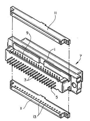
Referring to the drawings, Figure 1 shows a connector
which comprises a housing 1 and a plurality of contact pins
3 in two layers for connection at one end 5 to a plurality
of conductors of a wire bundle, for example by wire
wrapping, and for connection at their other end 7 to a
cooperating connector ~not shown). Each contact pin has a
spur pin 9 attached to it, which extends from the contact
pin and protrudes above a surface of the connector. A
module 11 is fitted on each surface of the connector such
that the spur pins 9 are received in recesses 13 therein.
Figure 2 shows a connector which comprises a plug shell
20 and a pair of wafars 21. Th,e wafers house contact pins
for connection to first and second sets of conductors. Spur
pins 23 protrude above the surface of the wafer to engage
recesses 24 in a module 25 which houses electronic
components. In u~e, the conductors of a flat cable are
connected to the contact pins of one of the wafers 21, the
module 25 is located on the spur pins 23, and the wafer is
inserted into the plug shell 20 for connection to an
appropriate socket, which may be connected to a piece of
electrical equipment or to another cab~e.
Figure 3 shows a connector which comprises a housing 31
having a contact pin 33 extending through it. One end 35 of
~2~7~3'7
MP1237 FF
-- 11 --
the pin extends beyond the housing for connection to a
conductor of a multiconductor cable, for example by means of
a solder. The other end 37 of the pin is recessed within
the housing, for mating with a corresponding pin on a
cooperating socket. A spur pin 39 is attached at one end to
the contact pin 33 and protrudes at its other end ab~ve the
surface of the housing, for connection to a module 41. The
spur pin and contact pin assembly is thus T-shaped. It is
preferably formed as one unit.
Figure 4 shows a connector which comprises a housing 51
having two L-shaped contact pins 53,55. One of the contact
pins 53 extends beyond the housing for connection to a
conductor oE a multiconductor cable. The end of the other
contact pin 55 is recessed within the housing, for mating
with a corresponding pin on a cooperating socket. Spur pins
57 are attached to each of the contact pirls and protrude
above the surface of the hou~ing. ~he spur pins 57 are
received within recesses in a module 59 which houses
electronic components, by means of which the spur pins, and
therefore also the contact pins, are interconnected.
.
Figure 5 shows a connector of the type shown in Figure 2
which comprises a connector shell 61 and a pair of wafers 63,
each of which houses contact pins 65 and spur pins 67. A
module 69 is located on the exposed principal surface of
each of the wafers 63 where they are electrically connected
to the spur pin~ 67. A layer of silicone rubbèr 71 is
located between the opposing surfaces of the modules and the
wafers for sealing the electrical connections b~tween them.
The modules and the wafers are forced towards one
another, so as to compress the layers of silicone rub~er and
~2~i7~7
MP1237 FF
- 12 -
therefore to enhance the seal between the modules and the
wafers, on insertion into the connector shell 61. This is
caused by the gradual decrease in the internal dimension of
the shell, from right to left as depicted in Figure 5 due to
the increase in thickness of the wall of the plug shell.