Note: Descriptions are shown in the official language in which they were submitted.
DE~lQNE~ES olJ BREVETS VOLIJMIINEUX
LA PRÉSENTE PARl~IE DE CETTE DE3UIANDE OU CE BRE~VET
CONIPIREND PLUS D'UN TOME.
' ...
CECI EST LE TONIE ~ DE ~
NOTE: Pour les tomes additionels, vauillez contacter le Bureau canadien des
brevets
~ ?~..
JUMBO APPLIC~TIONS/P~TENTS
THIS SEC:TION IDF THE APPLICl~TlONlPATENT C:Oq~lTAlNS MOR
THAN OINE VOLlJME
THIS IS VOLLIME / OF Z
NOTE: For additional volumes please contac~ the Canadian Paten~ Office
COMW:103
COMPUTER SYSTEMS SPEED CONTROL
AT CONTINUOUS PROCESSOR SPEED
This invention relates to personal comput~rs designed
with commercially available microprocessor chip sets.
More particularly, the present invention relates to a
personal computer in which the central processing unit
(microprocessor) is controlled to execute programs in a
variety of selectable speeds to achieve software ~ompat-
ibility with existing application programs which, because
of their specific hardware dependency, cannot be run at
higher speeds.
The present invention permits one to select speeds
ranging from execution speeds which simulate those below
original microprocessors such as the 8088/8086 micro-
processors (manufactured by Intel); speeds which simulate
advanced microprocessors such as the 80286 microprocessors
(manufactured by Intel); speeds which simulate the new
generation microprocessors such as the 80386 micropro-
cessors (manufactured by Intel) and any intermediate
speeds.
The introduction of the personal computer has re-
sulted in a tremendous amount of application softwareprograms written for both the professional and for the
~LZgl61~0`7
-- 2 --
home entertainment markets. These personal computers are
designed around commercially available microprocessor chip
sets which may include a plurality of microprocessors
connected in an architecture which results in varying
degrees of execution throughput ratesO
It has also been discovered that many of the cur-
rently used copy-protected schemes currently employed by
many of the software writers are dependent on micropro-
cessor clock rates. Many of the new personal computers
employing some of the new generation microprocessors with
high clock rates cannot utilize the copy-protected soft-
ware without data transfer errors.
Popular microprocessor chip sets widely used by
personal computer manufacturers are the Intel Corporation
8088 microprocessor; the 8086 microprocessor; and the
8028fi microprocessor, all having similar instruction sets.
Similar instruction sets are also available for a new
generation microprocessor from Intel, the 80386 micro-
processor. The 80386 microprocessor has a substantially
higher execution cycle rate than its predecessors, almost
three time faster than the 80286. Available also from
Intel is a co-processor chip, the Intel 80287, which may
be used either with the 80286 or the 80386 microprocessor
chips to achieve even higher execution throughput rates.
Also available is a 80387 co-processor, however, this co-
processor is not commercially viable at the present time.
With the availability of a software compatible
microprocessor (i.e., executes the same instruction sets),
it is possible to upgrade a prior art personal computer
with personal computers with higher execution speeds and
maintain compatibility with some application programs
- written for the lower speed microprocessor chip sets.
While faster software compatible microprocessors are
available, it is not possible, however, to simply substi-
tute the faster microprocessor for the slower micropro-
cessor and thereby produce a personal computer which
2~307
-- 3
executes at a higher speed for all of the application
programs written for the slower microprocessor.
Not all application programs written for the slower
microprocessors, i.e., 8088/8086 and 80286 micropro-
cessors, are capable of running at faster microprocessorspeeds even though each instruction in the program is
executed in a similar manner in these machines. The
inability to run some programs at higher speeds results
from the fact that programmers, when writing application
programs (third party software) for the slower micropro-
cessors, take advantage of the particular execution cycle
time in structuring routines which are time dependent.
For example, video game programs rely upon the normal
execution cycle time for the microprocessor in generating
time intervals which are necessary for the programs to
perform its various functions. Running the program at
higher instruction execution speeds changes the resulting
time intervals and thereby renders the program non-
functional. Application programs which are not dependent
upon the execution speed typically can be run at those
higher execution speeds and obtain the same results.
Similarly copy-protected programs rely on normal
execution cycle times for the microprocessor in generating
time intervals which are necessaxy for the program to
perform its various functions. These copy-protected
programs do not function properly whenever the instruction
execution speeds change.
It is undeniable that providing a personal computer
capable of executing application programs written for
slower microprocessors in a third of the time would be of
a commercial advantage in the marketplace, but such a
devi~e would not be commercially viable unless it were
able to execute a majority of the application programs
written for slower speed microprocessors. For example, it
is possible to provide a personal computer having an Intel
80386, 802B7 microprocessor pair (high speed micropro-
~Z91~i8~)7
-- 4 --
cessors) rather than an 80286, 80287 microprocessor pair(slower speed microprocessors) and run the high speed
microprocessor at di~ferent clocking frequencies (rates),
high speeds for those application programs which can run
at the higher speeds and slower speeds for those appli-
cation programs which are time dependent. Unfortunately,
this simple clocking speed change does not result in a
personal computer which is software compatible for all
~arieties of application programs.
It should also be realized that a change of the clock
rate (microprocessor frequency) will not suffice because
of the many other machine functions which may be affected.
Even though the previous microprocessor chip sets,
(i.e. 8086, 8088, 80286) are software compatible, the
internal design of the microprocessors is not the same.
This difference in internal design, depending upon the
design of the application program, i.e., does it contain a
lot of program jumps, affects the execution speed of a
given application program. The execution time at the high
speed for the high speed microprocessor is not necessarily
proportionally faster than the e~ecution time when micro-
processor clock is set to the slower normal frequency for
the slow speed microprocessor. Stated differently,
reducing the microprocessor clock from a high speed mode
- 25 to the normal clock for the slow speed microprocessor
while keeping all else the same does not result in the
same execution time for a given application program to run
on the high speed microprocessor as occurs if the same
program is run on the slow speed microprocessor.
For the Intel 80386 microprocessor, simply reducing
the clocking frequency to the clocking frequency of an
B088, or 8086, or 80286 microprocessor results in an
execution speed which is faster than it would have been
~or the slow speed 8088 microprocessor chip. This faster
execution speed results from the internal design differ-
ences which exist between the microprocessors, and the
r~ 12~6~
-- 5 --
fact that the 80386 requires 32-bit fetches from memory
while the 8088 requires 8-bit fetches, the 8086 requires
16-bit fetches and the 80286 requires 32-bit fetches using
two 16-bit parallel paths.
The internal design difference between these micro-
processors is primarily in the amount of pre-fetch buffer
memory provided in the microprocessor. In the Intel 8088,
there are four bytes of pre-fetch queue, in the 8086,
there are 5iX bytes of pre-fetch queue, in the 80286,
there are 8 bytes of pre-fetch queue while in the 80386
there are 12 bytes of pre-fetch queue. Each microprocessor
is designed to keep its pre-fetch ~ueue full of informa-
tion in order that the microprocessor can continue to
execute code, which on the average, achieves a desired
execution throughput rate. When program jumps occur, the
contents of the pre-fetch buffer are lost. This loss of
information is reflected in wasted execution time because
of the time required to obtain the pre-fetch information
that is discarded at the time the program jump occuxs.
Thus, the 8088 microprocessor, having four bytes of pre-
fetch queue running at a given clocking frequency and
fetching 8-bit bytes per fetch cycle would produce differ-
ent execution throughput than the 80386 having 12 bytes of
pre-fetch queue running at the same clocking frequency but
fetching 32-bit bytes per fetch cycle. It is because of
this difference in the pre-fetch buffer capacity and the
rate at which 32-bit bytes are fetched from memory that
the 80386 runs at a faster speed for the same application
program when the 80386 microprocessor is run at the same
clocking frequency as is normally used for the slower
microprocessor, e.g., 8088.
~ herefore, it would be advantageous to provide a
personal computer which provides for a high speed micro-
processor to execute application programs which are not
time dependent at high speeds, but provides a lower speed
execution for those application programs which are time
-- 6
dependent so that the time dependent application programs
appear to be running at substantially the same execution
speed as they would have run on the microprocessor for
which they were written.
In accordance with the present invention, there is
disclosed a personal computer having a high speed micro-
processor that is responsive to a mode select signal for
executing at a variety of selectable speeds thereby
permitting application programs written for a slower speed
microprocessor to be run on a high speed processor as well
as to give one the benefit of performing high speed
microprocessor functions for programs not time dependent
and/or for programs written with the high speed micro-
processor clock rate in mindO
In accordance with the present invention the personal
computer embodying the invention is further equipped with
an automatic speed control feature which simulates the
microprocessor speed for older generation microprocessors.
The speed control system or feature automatically detects
the occurrence of timing-dependent programs and adjusts
the overall program execution speed, thereby simulating a
system speed compatible with copy-protected software
and/or floppy ~iskette operations.
In accordance with the present invention the speed
control mechanism is also manually selectable and can be
manipulated by a computer operator to achieve system
speeds from those below an 8088 microprocessor through the
full system speed for an 80386 microprocessor.
It is an object of the present invention to implement
the invention in hardware, software or any combination
thereof. It is a further object of the present invention
to achieve the simulation of slower microprocessor speeds
by varying the length of the "STOP" or "HOLD" state of the
microprocessor. Thus the microprocessor clock rate is not
changed as done in other prior art machines.
~ ;~96~7
-- 7 --
The invention embodied in the personal computer
described herein further includes a 32-bit RAM memory and
a 16-bit ROM memory, each memory having a word comprised
of a plurality of bytes, and a microprocessor clock
generator running at a constant rate of 16 MHz. The
system speed is adjusted by varying the length of th~
microprocessor "STOP" state not the microprocessor system
speed of 16 MHz.
The invention embodied in the personal computer
described herein also includes a logic means responsive to
the speed select signal for controlling the length of the
STOP state of the high speed microprocessor when in a
slower than full speed mode. In this manner, the high
speed microprocessor executes time dependent application
programs in a slow mode without affecting the micropro-
cessor clock rate of 16 MHz.
For a fuller understanding of the present invention,
reference should be had to the following detailed descrip-
tion of the preferred embodiment of the invention taken in
conjunction with the accompanying drawings in which:
FIGURE 1 is a functional block diagram of the archi-
tecture of the present invention;
FIGURE 2 is a simplified logic diagram illustrating
the logic sequence employed in the microprocessor speed
adjustment invention;
FIGURE 3 is a timing diagram for various signals of
the microprocessor speed control logic and the HOLD
request and RESE~ request signals which occur during
different cycle operations;
FIGURE 4 is a simplified schematic illustrating the
basic logic steps employed to implement the microprocessor
speed control.
FIGURES 5A and 5B comprise detailed partial circuit
diagrams of a portion of the schematics;
FIGURE 6 comprises a detailed partial circuit diagram
of a portion of the DRAM memory board schematics; FIGURE
-- 8 --
7 is a simplified flow diagram o~ the HOLD/RESET arbitra-
tion logic; and
FIGURE 8 is a block diagram of the functions included
on the system board.
Similar reference numerals refer to similar parts
throughout the several views of the drawings.
Through the following detailed description of the
preferred embodiment of the present invention, and shown
in the accompanying drawings, the following notation has
been adopted for indicating signals. Since the terms "1"
and "0" and "true" and "false" can be ambiguous, their use
is avoided. In their place the terms "logic high" (H) and
"logic low" (L), in association with "active" and
"inactive" states for how the signals have been used. An
asterisk (*) following a signal name indicates that the
signal is "active" when low. For example, the HOLD
request signal to the microprocessor is designated HRQ*
and is active when at a logic low state, while the REFRESH
signal designated as REFRS and is active when in a logic
high state. The signals are "inactive" when in the logic
state opposite to its "active" logic state. In our
example, HRQ* is inactive when in the logic high state,
and the signal REFRS is inactive when in the logic low
state.
Certain logic circuit functions of the preferred
embodiment of the present invention have been constructed
using Programmable Array Logic (PAL) chips in implementing
the combinational logic required to combine certain ones
of the logic signals to obtain additional logic signals.
For such devices and where necessary to practice the
present invention, the combinational logic circuits
implemented with the PAL chips are neither shown in the
drawings or discussed in the specifications; however, the
logic design data for producing each PAL chip contained in
the invention and illustrated in the drawings is provided
in thi~ specification as an appendix. The PAL design data
07
,,
g
presents the logic equations for combining the input
signals to produce the output signals indicated in the
drawings. For these design equations and the type of PAL
chip to be programmed, it is possible to produce the
particular chip using standard manufacturing techniques
suggested by the PAL chip manufacturer.
A speed control feature of the present invention has
been implemented in the preferred embodiment to provide
compatibility with a number of software products that
contain programs dependent on certain system speeds.
Typically, these programs contain timing idiosyncrasies
associated with diskette copy protection mechanisms. The
system speed control hardware in the pre~erred embodiment
can also automatically detect the occurrence of timing-
dependent programs and thereby adjust the overall programexecution speed to simulate a system speed compatible with
the copy protection mechanisms. The speed control func-
tion described herein is also use~ul for adjusting the
personal computer program execution speed to handle action
software games written for 8088-based personal computers.
Reduction of the system speed to simulate the system speed
of an 8088-based personal computer allows these games to
be played at a realistic speed.
The simulated system speed control is accomplished by
reducing the system bus bandwidth using extended REFRESH
cycles. Since the CPU is in a HOLD state during REFRESH
cycles, the apparent execution speed of programs is
reduced as the length of the REFRESH cycles are increased.
The lengthening of the REFRESH cycles, however, has been
carefully implemented so as not to reduce the DMA latency
period that would be present during REFRESH cycles of
normal length. A DMA request for access to the bus cycle
is granted access to the bus immediately, since the CPU is
already in ~he HOLD state. The amount of time added to
the normal REFRESH cycle period i5 determined by the
~ ;~9~ 7
-- 10 --
length of a one-shot time period output ~y one of the
Intel 8254 timers in the system.
A RESET/HOLD arbitration circuit has been implemented
in the preferred embodiment of the present invention by
adding a flip-flop arbitration circuit to the HOLD and
RESE~ lines to prevent these signals from occurring
simultaneously. This arbitration circuit causes a RESET
signal to wait until after any pending HOLD request is
serviced or causes the HOLD signal to wait until after the
RESET is completed, depending on which signal is received
first at the input to the arbitration flip-flop~
The implementation of the RESET/HOLD arbitration
circuit in a personal computer with an 80386 micropro-
cessor restores compatibility to application programs,
written for an 80286 microprocessor, which utilized the
extended address space of the microprocessor in what is
called the "protected" mode. Application programs which
used the extended address space of the microprocessor in
the "protected" mode can only return to the "real" mode by
resetting the microprocessor. The RESET of the micropro-
cessor in the 80286 chip was accomplished by a feature
which allowed the CPU RESET without upsetting the state of
the rest of the machine. Upon RESET of the microprocessor
the processor returned to the "real" mode.
The chip designers of the 80386 eliminated the
processor's ability to recognize and respond to a "HOLD"
request from external hardware even during the processor
RESET. The HOLD state is used for system REFRE5H of
Dynamic Random Access Memory (DRAM) and for Direct Memory
Access (DMA). Thus these operations, DRAM REFRESH andDMA, cannot occur during RESET of the 80386 processor.
Since third party application programs were written with
these processor features in mind (i.e., DRAM REFRESH and
DMA), during processor reset, the 80386 microprocessor
which eliminated these features was incompatible with
pre-existing programs.
~1~9~7
-- 11 --
The arbitration circuit implemented in the preferred
embodiment of the invention permits the DRAM REFRESH and
DMA operations to properly operate during processor reset.
Thus compatibility with third party software which imple-
mented these features is assured with the 80386microprocessor.
A dual mapping BIOS function is implemented in the
preferred embodiment by using some of the high performance
Random Access Memory (RAM) to hold the BIOS stored in ROM.
Utilization of the RAM to store the BIOS improves the
performance of the 80386 microprocessor since the micro-
processor accesses a 32-bit memory (RAM) instead of the
16-bit memory (ROM). In prior art personal computers
software (BIOS) has been contained in ROM connected to the
microprocessor at the microprocessor's normal data size,
i~e., 8-bit ROM for 8-bit processor such as the 8088 and
two 8-bit ROMs for the 16-bit microprocessor such as the
8086 and 80286 processors. These 8 and 16-bit ROMs were
fast enough in access time to meet the requirements of the
prior art processors 50 the ROM's did not affect system
performance to any degree.
With the development of the 32-bit 80386 micropro-
cessor the standard 8 and 16 bit ROMs were too 510w to
keep up with the microprocessor. The addition of two more
ROM devices (to achieve a 32-bit bus width) presents an
undesirable cost penalty, however, a 16-bit ROM on a
slower 16-bit bus materially affects the speed advantage
of a 32-bit microprocessor.
Implementation of a dual mapped BIOS provides a 32-
bit RAM memory for the BIOS at no significant cost penaltysince the 16-bit ROM~ are not replaced. Use of 32-bit RAM
can be fully cost justified since the RAM subsystem
necessary for a 32-bit processor required a minimum of
1024 kilobytes. Since a majority of the applications
software can only utilize 640 kilobytes of RAM, 384
- 12 -
kilobytes of high performance RAM was available for use by
the BIOS.
To achieve compatibility with prior art machines, the
BIOS code has to remain at its original address and must
be protected from an inadvertent write-over.
The dual mapped BIOS has been implemented in the
preferred embodiment by adding decoding logic to the RAM
subsystem to al~low the system to respond to the ROM
addresses. The decoding logic operates through a writable
control port which switches the system from operation out
of the 16-bit ROM to operation out of the RAM.
Implementation in the preferred embodiment is accom-
plished in the following sequence:
1) Computer power up;
2) Execution of BIOS stored in ROM begins;
3) Part of RAM system is tested;
4) BIOS copied from ROM to RAM which has been
tested;
5) Control bit written by ROM code causing BIOS
restored in RAM to continue start-up of machine;
6) BIOS stored in RAM is write protected;
7) Machine boot-up and continues operation out of
RAM .
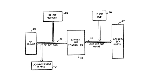
Turning now to the Figures, and first to FIG~ 1,
there is shown a functional block diagram of a personal
computer in accordance with the present invention. The
personal computer is designed around the central pro-
cessing unit (CPU) comprised of microprocessor (CPU) 20
and co-processor 21 (hereafter sometimes referred to as
numeric processor). For the preferred embodiment of the
present invention, microprocessor 20 is an Intel
Corporation 80386 microprocessor and the numeric co-
processor 21 is an Intel Corporation 80287 microprocessor.
It is also possible to substitute the 80287 microprocessor
with an Intel 80387 microprocessor when those micropxo-
cessors become commercially available.
- 13 -
Processor 20 and co-processor 21 are functionally
connected to a 32-bit data bus 22. A 32-bit Random ~ccess
Memory (RAM) 23 is also connected to the 32-bit data bus.
In order to permit the 32-bit processor 20 and co-pro-
cessor 21 to function with the older generation productsconsisting of 8-bit and 16-bit input and output devices a
bus controller 24 is provided between the 8/16-bit bus 25
and the 32-bit bus 22. The bus controller ~4 re-struc-
tures data from 8-bit and 16-bit devices into a data
string which can be accepted and used by the 32-bit
devices attached to the 32-bit bus 22.
The bus controller 24 likewise re-formats the 32-bit
data in a format which can be accepted and used by the 8
and 16-bit devices attached to the 8/16-bit bus 25.
As is further shown in FIG. 1, a 16-bit Read Only
Memory (ROM) 26 is functionally connected to 8/16-bit bus
25. The ROM 26 is used to store the Basic Input/Output
System (BIO~). A copy of the BIOS is transferred to RAM
after the computer power is turned on and a partial RAM
system test is completed.
Also illustrated in FIG. 1 are the 8/16-bit
input/output device ports which are functionally connected
to the 8/16-bit bus 25. Data transferred from the 8 and
16 bit input/output devices to the 32-bit RAM 23 is re-
structured by the bus controller 24 before being stored inthe 32-bit RAM.
Intel Corporation has published documentation for its
80386 and 80287 processors. This documentation is essen-
tial to an understanding of the operation of Intel's
processors. Instruction sets and the information provided
in Intel's manuals is presumed to be firmly understood by
anyone attempting to practice this invention.
The preferred embodiment of personal computer which
implements this invention contains at least the following
hardware:
a) 80386 microprocessor;
- 14 -
72159-4
b) 32 MHz clock for the 80386 microprocessor;
c) A 4 MHz or 8 MHz clock for a co-processor;
d) An 8 MHz expansion bus compatible with an 80286
processor;
e) A 4 MHz clock for the ~MA subsystem;
f) Random Access Memory;
g) Read Only Memory; and
h) Input/output device slots.
It is to be understood that the above listing of hardware
requirements is not intended to limit the scope of the invention
but rather to describe the preferred embodiment.
To provide a full and complete disclosure of the
invention and to permit one skilled in the art to practice the
invention, the mother board schematics of the preferred embodi-
ment are attached hereto as Appendix A. The memory board
schematics of the preferred embodiment are attached hereto as
Appendix B. A bill of materials for the preferred embodiment of
mother board schematics is attached hereto as Appendix C. A
memory board bill of materials for the preferred embodiment is
attached hereto as Appendix D.
The various clock rates referred to in the schematics
are CLK 16, CI,K 24 and OSC. The system clocks are separated into
three sections. One is the CPU clock (32 MHz) for the 80386 and
it's associated circuits. Another is the 24 MHz clock which is
used for the numeric co-processor. The third is the 14.31813 MHz
block which provides software compatible system timing functions,
; a fixed frequency signal on the expansion bus, and the 8042
r~
- ~LZ968~7
- 14a -
72159-4
keyboard processor clock reference.
The CLK 32 signal is clock for the 80386 processor
(CPU). The CPU clock is provided by a crystal oscillator,
~L2961~07
.
- 15 -
CMOS buffer IC 174HC125), and an F74 flip-flop. There are
three outputs from these circuits, a 32 MHz processor
clock, a 16 MHz reference clock (ChKl6*) (which has the
same phase as the internal CPU clock), and a reset signal
which meets the setup and hold time requirements for the
80386. The CPU reset is always adjusted to the 16 MHz
clock so that the phase is properly matched to the CPU.
The 32 MHz clock and the CLKl6* signal are provided
to the 32-bit memory board for use in state machines
synchronized in the CPU.
The signal BCLK is a (approximately~ divide by two
from CLKl6*. This division takes place in the sub-state
machine P~L D4-STAT where the clock is also re-synchro-
nized to the CPU on each bus cycle. It is this adjusting
that leads to the "approximately" part of the divide by
two functions. The average frequency will be somewhat
less than 8 MHz. Transitions of BCLK occur on rising
edges of CLK16*.
The clock for the DMA subsystem is generated from the
rising edge of the BCLK clock by toggling a 74LS74 flip-
flop. The outputs (DCLK, DCLK*) will therefore have a
frequency of one half that of BCLK.
The CLK 24 signal is the clock for the 80287 co-
processor.
The clock source for the 80287 is developed from a 24
MHz crystal oscillator. The 24 MHz frequency (CLK 243 is
divided down in single 74HCl09 to provide either 12 MHz or
8 MHz for use by the numeric co-processor (80287). The 12
MHz frequency is divided again inside an 80287-3 to
provide a 4 MHz operating frequency. The 8 MHz has the
required 33~ duty cycle for direct use by an 80287-8
giving an operating frequency of 8 MHz. The choice of
frequencies is provided by switch S~1-3. Switch OFF
selects 8 MHz (80287-8), switch ON selects 4 MHz (80287-
3)-
-` lZ9t~ 7
- 16 -
System bus compatibility is provided by clock rate
OSC. The specific time dependent clocks in the system are
generated by a crystal oscillator at a frequency of
14.31818 MHz which generates the signal OSC.
The OSC signal is provided to the system bus for
compatibility with older generation computer products.
The OSC signal is also divided by two by the PCLK flip-
flop to provide a stable and unchanging frequency source
(7.1591 MHz) to the keyboard processor (8042). The PCLK
signal is in turn divided by six to provide a timing
reference for the system timer ~TIMCLK). This frequency
is 1.19318 M~7 and is compatible with the previous pro-
ducts for timing and speaker purposes.
The divide by six is done with a synchronous counter
which cycles though the counts of 1 through 6 and back
again. The counter is not specifically set on power-up
but will always cycle into the legal count sequence within
seven clocks.
The microprocessor addresses and data handling are
generally handled in the manner set forth below. Typi-
cally the processor begins a bus cycle by placing an
address and status on it's bus. This address will usually
com~ out even while the previous cycle is still in pro-
gress. Since most devices expect to see a valid address
for the duration of a bus cycle, it is necessary to latch
the address seen by the system bus. Some devices (notably
high speed memory) are already short on time to perform
their function therefore they overlap some of their
operations with others, (i.e., address decode). To allow
this, the system bus also provides a set of address lines
LA<23:17> which are not latched but which can provide a
greater setup time to perform decoding. The typical usage
of these lines i5 address decoding whenever the address
changes, and then latch the decoded outputs.
To provide the unlatched addresses, the board con-
tains buffer ICs which are connected to the CPU's
96~
- 17 -
PA<23:17~ address lines and provide LA<23:17> (see FIG. 8)
as an output.
To provide the latched addresses, the board contains
latched ICs which are connected the to CPU's PA<19:2> and
provide SA<19:2~ as an output. These latches are of the
fallthrough type so that when the Address Latch Enable
signal (ALE) goes active the address appears at the
output. When ALE goes inactive, the addresses will stay
on the outputs until the next bus cycle begins.
The address lines SA0 and SAl are handled differ-
ently. The CPU indicates which bytes are to be accessed
out of the 32-bit word by the status lines BE3* to BE0* or
Bus Enable three through 7ero. The output of this state
machine are the address lines SA0, SAl and BHE*.
The signal BHE* is used on the system bus to indicate
that the high half of the 16-bit data bus contains valid
data.
These signals (SA0, SAl and BHE*) are changed at the
rising edge of ALE so that their timing is very similar to
the other SA<19:2> address lines.
All of the address outputs listed above are disabled
when the CPU responds to a HOLD request (BHLDA) so that
another device can control the address bus. When this
occurs, the address lines are fed back to the CPU bus
(PA<23:2>> and BE<3:0>) so that the 32-bit memory board
can receive the address data from the other device. The
feed back operation occurs from the SA<16:0> and the
LA<23:17> lines through buffers and a PAL (~4-SADI) for
SA0, SAl and BHE*.
CPU address line PA20 is handled a little differ-
ently. Because of software compatibility considerations
(with 8088 products) it is sometimes necessary to restrict
program access to the bottom megabyte of memory. This is
done by disconnecting the PA20 line from the bus and
forcing a low in it's place (by means of a 74F257). This
is controlled by the line LOWA20 from the keyboard con-
L29~;8~
- 18 -
troller. To equalize the delay with the other address
lines, the output of the 74F257 is used to directly drive
the LA20 line instead of being buffered again by a
74LS245.
The CPU data bus is buffered from the rest of the
system by four bi-directional buffer ICs and four latches.
On the CPU side of the busl the 80386 and 80287 are
connected together. Four ICs buffer the separate bytes of
the data bus. The latches are used to hold read data for
the CPU during separate read cycles on the system bus when
the CPU attempts to read more data than the system bus
allows.
The data path also contains a bi-directional buffer
between the high and low half of the bus to enable routing
of the data from high half to low during high writes and
routing of the data from low to high half during high
reads of the 8-bit bus. This function is controlled by
the CPYEN* and CPYHL* lines. CPYEN* enables the buffer,
CPYHL* controls the direction according to the type of
cycle (active for CPU writes or DMA reads).
The last item in the data path is a buffer for the
processor board I/O devices. This buffer is normally
active in the "TO" direction to the I/O devices and
switches to the "FROM" direction when an I/O read occurs
to these devices (controlled by CIORD*). This buffer is
disabled when DMA operations occur to allow the bus to be
used by the DMA controllers for address latching.
Table I, attached hereto as Appendix E and incorpo-
rated by reference as if set forth herein in full, illus-
trates the bus conversion from the CPU's BE<3:0> lines tothe address lines and the data buffers that are enabled
for each conversion.
Note that in Table I the "X8" term means that the
system bus has indicated the cycle should be 8-bits. The
BEx* lines are negative true bus enables from the CPU.
The SAl and SA0 lines are positive true and BHE* is
-` ~L29~
-- 19 --
72159-4
negative true. The BENX* lines enable the data buffers to the
bus and the latching function from the hus, they are negative
true. The CPYEN* line enables the copy buffer from the SD~7:0~
to SD~15:8~, the CPYHL* lines is also enabled when reading (high
to low copy)~ The LAST CYCLE term is used to indicate the last
cycle in a group of cycles from one CPU status, it tells the state
machine to send the CPU the READY* signal.
The command cycles generated by the bus control logic
are listed in Table II attached hereto as Appendix F. The number
of 62.5nsec clocks is listed for a no-wait state cycle, normal
cycle, and one wait stàte cycle for each of the command types.
Both the total cycle time and the command active ton) time are
given. For cycles with more than one bus wait state, each wait
state adds two additional 62.5nsec clock cycles.
If the CPU status indicates more than one bus cycle
will be required for a single CPU access, then the bus state
machine will run the necessary number of bus cycles (duration
indicated in Table II) to complete the CPU access. For example,
if the CPU status indicates a double word memory read from the
8-bit bus, then the total cycles for the access would be 4*12=48,
62.5nsec cycles (assuming normal cycles).
In the preferred embodiment the CPU is normally held
in the NOT READY state. READY* only goes active (low) when a
cycle is guaranteed to be finished. The CPU next address (NA*)
line is normally inactive, requiring the logic to specifically
tell the CPU when to send the next address.
, ,, , 7,
- ~L2~1~8~'7
- l9a -
72159-4
The cycle begins when the 80386 activates ADS* and
presents the status lines. The address is decoded by the 32-bit
memory board (if present) and the signal M32* is produced. The
system board decodes the status lines to determine i the cycle
is a valid memory cycle, producing
- 20 -
the signal MEM*. M32* and MEM* are then combined to the
signal MEM32* which is latched by the rising edge of CLK32
(the CPU clock) at the beginning of phase one in the CPU
cycle following ADS* going active. If the end result of
this is NO~ a valid 32-bit memory cycles, the signal
MYCYC* goes active.
MYCYC* is then sampled by the D4-STAT PAL on the
rising edge of CLK16* (the bus clock). Unless otherwise
noted all clocks referred to are CLK16* clocks. When the
PAL clocks in MYCYC* it generates the signal ALE*~ The -
PAL code is set up to allow ALE* to be active only for a
signal cycle. What follows next is the propagation of the
ALE* pulse through a series of flip-flops arranged in a
configurable shift register. The general method is to
bypass parts of the shift register to shorten the total
bus cycle time depending on the type of bus cycle to be
executed.
The rising edge of ALE latches the address and status
for later use and does the SAl, SAO, BHE* generation.
This signal BCLK will be forced to a low during ALE by the
D4-STAT PAL to insure the compatibility with previous
products.
The next stage is T00. It is always generated. If
the command being generated is a 16-bit memory command, as
signified by LM-IO and M16*, then the signal CMD* will
also be set active at this time. CMD* is combined with
the decoded status to generate the signal MRDC* or MWTC*.
If this is the last cycle in a set, (either guaranteed by
the state or because the bus size is known by M16* and a
memory cycle) then the D4-SADO PAL will set the signal
CLSTD* active at this time.
The next stage is T01. It is always generated. If
the command being generated is not a 16-bit memory com-
mand, as signified by LM-IO and M16*, then the signal CMD*
will also be set active at time time. CMD* is combined
with the decoded status to generate the signal IORC*,
307
- 21 -
IOWC* or INTA*. If this is the last cycle in a set,
(because the bus size is known by IO16* and an I/O cycle~
then the D4-SADO PAL will set the signal CLSTD* active at
the time. If this is 16-bit memory cycle, and the NOWS*
signal was received during T00 (LNOWS* active), then the
signal BRDY* will be generated next to terminate the cycle
and no other stages will be activated.
The next stage is T10~ It is always generated. If
the cycle is a 16-bit memory cycle, then the T40 stage
will also be activated at this time. In this case, the
T10 and Tll states will be ignored for the remainder of
the 16-bit memory cycle.
The next stage is Tll. It will always be generated.
If the cycle is a 16-bit I/O cycle, then T41 will also
occur at the same time as Tll. If this is an 8-bit cycle,
and the NOWS* signal was received earlier (LNOWS* active),
then the signal BRDY* will be generated next to terminate
the cycle and no other stages will be activated. Other-
wise, stages T20, T21, T30 and T31 will follow if the
cycle is an 8-bit bus cycle as signalled by CX16*
inactive.
The next stage is T40. This stage is entered either
from T31 during an 8 bit cycle, or T01 if a 16-bit memory
cycle or a cycle that does not depend on the CX16* ~tatus
occurs. This stage is skipped if the LNO~S* line is found
active.
The next stage is T41. This is entered only from T40
(the normal case) or T10 (if a 16-bit I/O cycle is in
progress). If the signal WAIT* is active at the end of
T41, then T41 will be restarted, holding the bus in a wait
state. Since the WAIT* signal is developed by sampling
the BUSRDY* going high only every BCLK rising edge, wait
states will come in increments of two clock cycles. When
WAIT* goes inactive, the signal BRDY* will be generated to
terminate the cycle.
8~7
- 22 -
At the same time as the cycle is being terminated
(BRDY* is set active) several things can occur. If this
is not the last cycle in the set (CLAST* inactive), then
TS0* is set active by the D4-STAT PAL to start another
cycle. If this is the last cycle in the set (CLAST*
active) and another cycle is pending (MYCYC* is active),
then TS0* is set active by the D4-ST~T FAL to start
another cycle. If no more cycles are to be run for the
moment, then the bus state machine will remain idle
waiting for another cycle.
TS0* is used to provide an adequate address setup
between cycles in a group or between groups when the CPU
pipelines the next cycle. After TS0* the ALE state will
be entered for the next cycle.
The signal CMD* (which is used to enable on of MRDC*,
MWTC*, IORC*, IOWC* or INTA* ) iS started at the beginning
of T00 or T01 as discussed above. It will end at the end
of the basic bus cycle (when BRDY* or TS0 goes active).
The signal WDEN* is used for enabling the various
data buffers during write cycles. It goes active at the
same time as ALE and goes inactive one cycle after CMD*
goes inactive. In the case of back to back cycles, WDEN*
will therefor remain active until after the last CMD*.
The signal BRDY* from the D4-STAT PAL signals the Pnd
of a set vf bus cycles to the CPU. The signal CLSTD*
(which goes active for one CLX16* cycle to indicate that
the last cycle of a set is in progress) also generates the
CLAST* signal internal to the D4-SADO PAL. CLAST* is used
by the D4-SADO PAL to do the conversion from BE<3:0> to
SAl, SA0 and BHE*. CLAST* is also used to tell the state
machine that no more cycles are in the set. At the rising
edge of ALE, CLAST* is set to the inactive state in
preparation for the next CPU access.
The signal CLSTD* is also used to generate NAB* (next
address from bus) which signals the CPU that it is all
right to put a new address and status onto the CPU bus.
~2968~`q
- 23 -
72159-4
Since NAB* is sampled at the beginning of phase two of a CPU
clock cycles, it is synchronized to the rising edge of CLK32 at
the rising edge of CLK16* by a F175 flip-flop. This assures a
setup time to the CPU for NA*.
The signal CX16* is used to signal the presence of a
16-bit memory or I/O cycle. It is set active during T00 for
memory cycles if M16* is active. It is also set active during
T10 for I/O cycles if IO16* is active. It is set inactive at ALE
in preparation for the next cycle. This signal is used to
control the bus address conversion for the 8 or 16-bit bus and to
adjust the timing of the expansion bus for 16-bit operations.
The signal LOE* (latch output enable) is generated
during read cycles from the 8/16 bus to enable the data stored in
the data latches to the CPU data bus. LOED* is first set active
during ALE in the D4-SMSC PAL and is set inactive as soon as the
signal BRDY* is active. LOED* is then clocked through to LOE*
by the rising edye of CLX32 at the rising edge of CLK16* in a
74F175. When LOE* goes inactive, it buffers before the CPU may
begin driving the bus again. The total delay to disable the
latches is calculated in Table III attached hereto as Appendix G.
The BUSRDY signal is used to add additional wait signals
to a bus cycle. If a 16-bit device wants to add an additional
wait state, then it must pull the BUSRDY low (inactive) by the end
of the third CLK16 cycle after the falling edge of ALE. To add
only one wait state, BUSRDY must return to the high state during
the fourth CLK16 cycle after the falling edge of ALE. If an 8-bit
device wants to add an additional wait state, then it must pull
--~ lZ~ 7
- 23a -
72159-4
the BUSRDY low (inactive) by the end of the ninth CLK16 cycle
after the falling edge of ALE. To add only one wait state,
BUSRDY must return to the high state during the tenth CLK16
cycle after the falling edge of ALE. The decode logic to drive
BUSRDY should use the device address
, !
,.
~2~ 7
, ~
- 24 -
and MRDC*, MWTC*, IORC* or IOWC* as inputs. Synchronous
peripherals usually use the falling edge of BCLK as the
time to change the state of BUSRDY.
The NOWS* signal is used to shorten the standard bus
cycle. If a 16-bit memory device is to prevent the
standard wait state then it must pull the NOWS* line low
(active) within one CLK16 time from the falling edge of
ALE. (Note that this is not possible on 16-bit I/O cycles
because it is not known that an I/O cycle exists until the
required time). If an 8-bit device is to prevent the
standard wait states then it must pull the NOWS* line low
(active) within two CLK16 times from the falling edge of
the command. The decode logic to drive NOWS* should use
the device address and MRDC*, MWTC*, IORC* or IOWC* as
inputs. If less than the four standard wait states
normally used on 8-bit bus cycles is desired, then the
NOWS* line can be used to provide 1, 2, or 3 wait states
by delaying the activation of NOWS*. The NOWS* line is
sampled at approximately the falling edge of BCLK.
The M16* signal is used to indicate that the current
address on the LA<23:17> line is covered by a 16-bit
memory peripheral. The system board will only use this
signal if the current cycle is a memory cycle. The
addressed peripheral on the bus must pull the M16* line
low as soon as the address is decoded and hold it low
until the address becomes invalid. The M16* line must be
correct before ALE goes away to insure that it is latched
by the system board latch. Pulling this line low prevents
the 16-bit to 8-bit bus conversion logic from being
activated.
The IO16* signal is used to indicate that the current
address on the SA<9:0> lines is covered by a 16-bit I/O
peripheral. The system board will only use this signal if
the current cycle is an I/O cycle. The peripheral
addressed on the bus must pull the IO16* line low as ~oon
as the address i5 decoded and hold it low until the
:~2~8C~7
- 25 -
72159-4
address becomes invalid. The IO16* line must be correct by the
second CLK16 cycle after ALE goes away to insure that it is
latched by the system board latch. Pulling this line low
pre~ents the 16-bit to 8-bit bus conversion logic from being
activated.
The signals SMRDC* and SMWTC* are used by the 8-bit bus
only. These memory signals are only enabled when the lower one
megabyte of memory is addressed. They are developed from the
regular MRDC* and MWTC* signals by enabling a set of tri-state
buffers with the signal LOWEN*. This signal is developed by the
D4-SROM PAL from the address information on the system bus. The
PAL also includes the latching function required to hold the
address through the entire cycle and the refresh function for any
dynamic memory on the original 8-bit bus.
The state sequences for typical machine cycles for the
preferred embodiment are set forth in Table IV attached hereto as
Appendix H.
The processor board of the preferred embodiment (also
referred to as a mother board~ contains logic to generate other
types of bus cyclesO A listing of other types of bus cycles is
set forth in Table V attached hereto as Appendix I.
A description of the Input/Output (I/O) subsystems for
the preferred embodiment is set forth in Appendix J which is
; attached hereto.
A description of the interrupt controller subsystem and
interrupts for the preferred embodiment are set forth in Appendix
K which is attached hereto.
Q7
- 26 -
7215g-4
A description of the ROM memory system for the preferred
embodiment is set forth in Appendix L which is attached hereto.
The following description for miscellaneous subsystems
of the preferred embodiment are set forth in Appendix M, which
are attached hereto:
1) Expansion bus definition;
2) Bus timing information for expansion bus;
3) 32-bit expansion bus definition;
4) Bus timing information for 32-bit expansion bus;
5) Page mode dynamic RAM board;
6) Address decoding;
7) Jumper setting;
8) Bits presented by option board;
9) Detailed cycle description; and
10) Timing analysis for page DRAM board.
Turning now to Fig. 2 a simplified logic diagram
illustrates the system components of the speed control device and
the arbitration logic.
The speed control of the microprocessor can be
initiated by either the floppy drive motor spin-wp or enable 30
or the speed control software 31. The computer operator
interacts with the computer through a utility program to set the
speed of the microprocessor. This action by an operator is
represented in Fig. 2 by block 31.
As illustrated in Fig. 2 the floppy drive enable 30
is logically OR'ed with the software controlled speed control 31
and logically AND'ed with the speed control bypass switch 32. In
the event the bypass switch 32 is closed the speed control
.!
lZ~,t~ 7
- - 27 -
72159-4
mechanism is inoperative. The speed control command is then
logically AND'ed with the speed control timer 33, therefore, the
CPU HOLD output to the CPU remains active for as long as the
timer remains active.
The speed control command is logically OR'ed with the
arbitrated output of the arbitration logic of the DM~ request 34
and the REFRESH request 35.
The D~IA request/REFRESH request is arbitrated by
arbitrator logic 36 to prevent both a DMA and REFRESH request
from occurring simultaneously.
The HOLD request 37 to the CPU can be generated by
either the REFRESH request, DMA request or the speed control
logic. As will be described infra these holds cannot occur
simultaneously because of the logic which controls each function.
The speed control is initiated by the following four
CPU instructions:
l) MOV AL, 92H
2) OUT 4BH, AL
3) MOV AL, XX
4) OUT 4AH, AL
Instructions l and 2 above essentiallv disable the
component 8254. "XX" in instruction 3 above is a number from 2
to 38 hex. The one-shot time delay set in the speed control
timer is set by instruction 4. Address 4AH in instruction 4
above represents that timer 2 is to be set to the value in
register AL. Address 4BH in instruction 2 is the control word
re~ister.
lZ~fi~ 7
- 27a -
72159-4
The speed adjustment software controls the setting of
the one-shot timer. The source code listing of this utility
program is set forth in Appendicies N and O attached hereto.
Utilizing the utility programs set forth in
Appendicies N and O the operator of the machine selects a time
delay setting by selecting one of the arbitrary designations set
forth below:
COMMON
FAST
. .
,
- 28 -
HIGH
or by selecting a speed setting from 1 to S0 where the
setting "1" corresponds to the slowest machine speed which
can be simulated by this microprocessor and "50" corre-
sponds to the highest speed which can be simulated by thismicroprocessor.
It should be noted that the designation "COMMON" will
simulate a microprocessor speed equivalent to an 80286
microprocessor operating at a 6 MHz clock rate; the
designation "FAST" will simulate a microprocessor speed
equivalent to an 80286 microprocessor operating at an 8
MHz clock rate; the designation "HIGH" will simulate the
microprocessor speed of an 80386 microproce~sor operating
at the 16 MHz clock rate; full speed of an 80386 micro-
processor.
The arbitrary speed designation of "3" on a scale of1 to 50 corresponds to the simulated speed of an 8088
microprocessor and the arbitrary speed designation of "50"
on a sale of 1 to 50 corresponds to the designation "HIGH"
described above.
The KSUBS source code attached hereto as Appendix N
sets the one-shot timer by setting register AL to the
required hexidecimal value which corresponds to an oper-
ator's selection of either a value of "COMMON, "FAST" or
"HIGH" or by an operator's selection of a decimal number
in the range of 1-50.
The timer source code attached hereto as Appendix O
sets the one-shot timer by setting register AL to a
hexidecimal value corresponding to the "FAST" mode when-
ever the floppy drive motor is enabled. Enabling thefloppy drive motor reduces the apparent microprocessor
speed since most floppy drive operations indicate either a
transfer of data from a copy-protected diskette or other
diskette operation which cannot be performed at the full
80386 processor speed.
~` ~2~ 7
- 29 -
Turning now to FIG. 3 and FIG. 4 the following
sequence is illustrated in FIG. 3 (timing diagram) (the
numbers in the description below corresponding to the
numbers on the timing arrows shown in FIG. 3):
A 4 MHz clock rate is illustrated as "DCLK". Each
square wave represents 250 microseconds.
3-1: The REFRESH request occurs once every 15
microseconds. This request is arbitrated with the Direct
Memory Access (DMA) request to prevent simultaneous
requests. The REFRESH request is then logically OR'ed
with the other request sources to generate the CPU "HOLD"
request.
3-2: 90metime after the HOLD request is
generated and after the current CPU bus cycles have been
completed ~approximately 215 nanoseconds to 12 micro-
seconds later) the CPU will stop executing the program and
grant the HOLD acknowledge (ACK).
3-3: The HOID ACK is logically gated with the
arbitrated REFRESH request to form the REFRESH acknowledge
IACK) signal to the REFRESH controller.
3-4: The REFRESH ACK signal triggers the
digital one-shot (Intel 8254 or similar logic device)
which in turn sets the STOP request signal active. Since
the REFRESH request is still present (high), there is no
chan~e in the CPU state.
3-5: The REFRESH controller executes the
REFRESH cycle on the system bus and then releases the
REFRESH request. This typically takes approximately 500
nanoseconds.
3-6: Release of the REFRESH request also
releases the REFRESH ACK signal and ends the REFRESH
portion of the cycle. tIf the STOP request is NOT
present, then the HOLD request is released and the CPU
begins executing againO
3-7: During the duration of the one-shot
timeout, the STOP request remains active and the CPU
~Z~ 7
- 30 -
cannot run bus cycles (i.e., execute code). This timeout
value is variable from 0 duration (e.g., CPU begins
executing immediately after RE~RESH, equivalent to full
speed microprocessor cycle) through 15 microseconds where
the CPU never gets a chance to execute because another
REE'RESH and STOP cycle will begin as soon as the last
cycle is completed (e.g., microprocessor fully stopped).
Choosing values between 0 and 15 microseconds will result
in apparent speed changes of the CPU from full speed to
the speed of previous generation microprocessors. If the
time delay value for the one-shot timer is less than 15
microseconds the STOP request will be dropped when the
one-shot times out.
3-8: Release of the STOP request causes the
HOLD request to be dropped.
3-9: The CPU responds by dropping the HOLD
ACK. The CPU begins executing the program again (i.e.,
executing code or program steps).
3-10: 15 microseconds from the original REFRESH
request, the next RÆFRESH request will arrive and the
cycle will repeat itself.
The DMA (Direct Memory Access) subsystem is not
impeded from normal operation during the time the CPU is
stopped to permit the simulation of a slower CPU. Devices
; 25 using the DMA subsystem are therefore independent of the
simulated speed of the CPU.
The use of the microprocessor HOLD or STOP permits
time dependent operations to be handled by the 32-bit
microprocessor which is operating at a constant clock
rate, in this case 16 MHz, without slowing the micro-
processor down to a slower clock rate. The use of a
slower clock rate has been previously suggested however
this method of operating is not acceptable in an 80386
environment because it has the effect of slowing down all
operations, not just those which are time dependent. Thus
in the typical application the microprocessor is placed on
,
--` 12~fi~
- 31 -
HOLD only for so long as necessary to simulate the micro-
processor speed which is selected by an operator or the
speed which is necessary to perform time dependent
functions.
Alternatively, the operation of the microprocessor
can be placed in a deliberately slow mode by causing the
one-shot timer to be re-initiated as soon as it is
released. This is accomplished in software and is initi-
ated by the operator calling up a "Mode Speed" subroutine.
The "Mode Speed" source code is provided in Appendix N as
"KSUBS". Once the subroutine is called up the operator
selects a speed ranging from 1 to 50, or in the alterna-
tive specific speed designations which have been arbi-
trarily set. In this case the following speeds have been
arbitrarily set which correspond to the speeds indicated
below:
COMMON - Approximately equivalent to a speed
setting of an 80286 microprocessor
operating at clock rate of 6 MHz
FAST - Approximately equivalent to a speed
setting of an 80286 microprocessor
operating at a clock rate of 8 MHz
HIGH - Approximately equivalent to a speed
setting of an 80386 microprocessor
operating at a clock rate of 16 MHz
The manual setting of the speed as described above
permits the operator of the computer to play time depen-
dent games and also to execute time dependent programs
without losing the benefit of having a 32-bit micro-
processor operating at a clock rate of 16 MHz.
Example 1
The following example illustrates the approximate
microprocessor speed which is simulated when the one-shot
timer time delay is set at 2 microseconds:
;
-
- 32 -
~0.5 + 2
1 - 15 = 86
0.5
1 - 15
where the denominator of the above equation sets forth the
normal system speed with the microprocessor operating at
full system speed, i.e., the 16 MHz clock rate, and the
numerator of the above equation is the effect of the
slow-down on the system speed.
In the above equation normal system speed is desig-
nated by unity and the two microsecond one-shot timer
setting is entered in the numerator of the equation.
The system speed which is simulated is 86% of the
full 80386 microprocessor operating at the 16 MHz clock
rate.
Referring now to FIG. 4 a simplified schematic of the
arbitration logic and speed control logic is illustrated.
The CPU HOLD request can be generated by either the
arbitrated REFRESH request, the arbitrated DMA system
request or the system speed control.
The system speed control is initiated by software and
occurs by either a manually initiated speed selection 31
or by operation of the floppy diskette drive 30.
As illustrated in FIG. 4 the speed control is logi-
cally AND'ed with the one-shot to generate the CPU HOLD.
The implementation of the one-shot provides the time delay
necessary to stop the CPU for a specified time to
"simulate" a microprocessor speed below that which corre-
30 sponds to an 80386 microprocessor. The longer the time
delay of the one-shot the slower the CPU "appears" to
operate. The CPU speed is not reduced but rather only
"appears to be reduced" since the CPU clock rate is not
reduced but rather the CPU is stopped and started thereby
generating an average CPU time which "appears" to be
slower.
- 33 -
Referring now to FIG. 5A the one-shot timer 33 is
represented by device U41. The output of device U41,
SLOWQ* is logically AND'ed with SLOWD* at device U79D and
inverted by device U65A to produce the SLOWH* output.
The by-pass around the automatic speed control is
provided by switch 38 designated as SWl in FIG. 5A. With
switch 38 open the automatic speed control is enabled
whenever the floppy drive is activated. Conversely with
switch 38 closed the automatic speed control is bypassed.
FIG. 5A also illustrates flip-flop 39 also designated
as device U78A. Flip-flop 39 serves as the arbitration
logic for the DMA request and the REFRESH request. The
flip-flop 39 also provides the CPU HOLD request to the CPU
20 for the speed control function.
Referring now to FIG. 5B the functional schematic for
the RESET/HOLD arbitration logic is illustrated. The
arbitration circuit operates on the HOLD and RESET signals
to prevent them from occurring at the same time. The
arbitration circuit causes a RESET signal to wait until
after any pending HOLD is serviced or causes a HOLD signal
to wait until after the RESET is complete. The arbitra-
tion circuit holds the last signal received until the
first signal received is complete.
The preferred embodiment of the invention is illus-
trated in the drawings attached hereto as Appendicies A
and B. In this embodiment the speed control system is
implemented to give the user some control of the system
speeds in the event that software is speed dependent. The
system consists of one channel of the second 8254 timer
counter and an interconnect to the HO~D request circuit.
The timer channel is programmed as a one-shot which is
triggered by REFRESH requests. If the 8042 keyboard
controller SLOWD* line is active (LOW) then the timer
output will extend the CPU HOLD time for REFRESH by the
programmed value of the one-shot. During this HOLD time,
the CPU cannot use the bus for execution, but the DMA
Q~
- 34 -
subsystem can continue to work. The time is clocked by
DCL~ giving a 250 nanosecond increment in bus HOLD time.
To disable the circuit, the 8042 SLOWD* output can be set
inacti~e (HIGH) or the 8254 timer can be stopped by
programming the counter but not giving it a count value.
In order to minimize the potential for operator error
because of a failure to set the speed at the proper rate
for floppy diskette operations, the computer software is
specifically written to sense the operation of the floppy
diskette motor. In actuality the software detects a call
to the diskette motor or drive and initialiæes the one-
shot timer by setting the one-shot timer time delay. This
in efect slows the operation of the computer to a rate
equi~alent of COMMON. Any calls to the diskette for
information which is to be transferred at the 16-bit rate
will result in an automatic slow-down of the micro-
processor, not by slowing down the clock rate as pre-
viously done in prior art devices but by initializing the
one-shot timer described above and thus placing the
microprocessor on HOLD. This has the net effect of
holding up execution of any bus cycles for a pre-deter-
mined period of time.
Once the transfer of data is completed the HOLD is
released and the microprocessor resumes it operation and
execution of bus cycles. The completion of data transfer
is sensed by the software by monitoring the floppy
diskette drive motor - thus after the diskette drive motor
is stopped the initialization of the one-shot timer is
halted and the microprocessor resumes unimpeded operation.
It has been found that copy-prote~ted diskettes are
very sensitive to the execution speed of the micro-
; processor primarily because the copy-protection scheme is
expecting a particular timing rate. Thus as software
written for an older generation machine i adapted for a
faster new generation machine it becomes difficult to use
the copy-protected software in the new generation machine
~ fi~q
- 35 -
because the software which was written to execute in a
slower machine is expecting a particular execution rate
which was determined by the slower clock rate. It has
been found that the copy-protected software written for
older, slower machines cannot be executed in newer, faster
machines because of the faster clock rates. In the
present invention the utilization of the one-shot timer to
stop execution of the microprocessor by placing it in the
HOLD or STOP state permits the older software written for
the slower machines to be utilized in this new machine
without slowing the clock rate down to that of the older
generation machines. Thus the new generation machine
which is operating at a clock rate of 16 MHz and a 32-bit
rate achieves compatibility with older software which
heretofore had not been compatible with a new generation
machines.
The ability of a new machine to adapt to older
generation software has added advantages in that there is
no need for the prospective customer of the computer to
wait for application programs to be written for the new
machine by third party programmers writing with the new
clock rate in mind. Thus a 32-bit machine operating at 16
MHz has the potential to gain ready acceptance from future
users because it is fully compatible with software pro-
grams previously used by the prospective customers in theolder generation machines.
The utility program which can be executed by the
operator of the machine to slow down the machine has the
added advantage that it will permit the operator to vary
the program speed not by changing the microprocessor clock
rate but by varying the time delay of the one-shot timer.
This advantage is manifested in the ability of the oper-
ator to manually and intentionally vary the speed of the
machine in the event that he wants the machine to function
as an older generation machine.
- 36 -
A switch SWl also provided as is illustrated in FIG.
5A which permits the operator to manually select a bypass
mechanism. This switch will defeat the automatic slow-
down of the machine. Thus the software which is written
to slow-down the operation of the machine by sensing the
operation of the floppy diskette drive is defeated.
As previously described the operation of the machine
can be manually set to operate at a rate much slower that
the rate achieved with a 16 MHz clock rate by selecting
the one-shot timer to a time delay which simulates the
operation of a slower machine, l.e., an 8088 or 8086
microprocessor or an 80286 microprocessor. A source code
listing is provided and is fully set forth in the
Appendix H.
The source code of the software listing is provided
in Appendix O for the subroutine which is executed to
automatically set the speed of the machine. This auto-
matic feature automatically detects the operation of the
floppy diskette motor and sets the speed of the one-shot
timer to a simulate the speed of an 80286 microprocessor
operating at a clock rate of 6 MHz.
An excerpt of the schematic necessary to implement
this invention is set forth in FIG. 5A and 5B, however,
the entire operational schematics of the preferred embodi-
ment are set forth in Appendicies A and B. It is to be
understood that the schematics merely set forth the
preferred embodiment of the invention and that further
implementations of this invention may be made by one
skilled in the art.
It is to be further understood that the software
listings set forth in Appendicies N and O are merely
illustrations of the one embodiment of the invention and
that further embodiments may be realized and implemented
by one skilled in the art.
To assist in the interpretation of the schematics
attached hereto as Appendicies A and B, a bill of mate-
~ z9~7
- 37 ~
rials of the components used in the preferred embodiment
are attached hereto as Appendicies C and D. Again it is
to be unde,rstood that the components set forth in these
Appendicies are merely the components used in implementing
the preferred embodiment.
A simplified logic diagram is set forth in FIG. 4.
The simplified logic diagram illustrates the logic flow of
each of the components necessary to implement the pre-
ferred embodiment. It is to be understood that the
implementation of the preferred embodiment may be accom-
plished in a manner other than that specifically illus-
trated in FIG. 4 by those skilled in the art. The auto-
speed routine is executed by calling up the speed-mode
routine which is set forth in Appendix N. The routine is
executed by utilizing the following command "Mode Speed".
Upon execution of this command the routine is auto-
matically loaded and thereafter the operator causes the
program to execute by entering a number from 1 to 50 or
one of the following commands: COMMON, SLOW or FAST.
As previously indicated the utili~ation of one of the
word commands above results in the assignment of a speed
destination by the software. Upon assignment of the
assigned speed setting the software causes the entry of
the specified speed assignment into the one-shot timer.
Consequently, a corresponding time delay is assigned to
the one-shot timer thereby causing a corresponding time
delay and HOLD of the execution of microprocessor bus
cycles.
As previously indicated the 80386 microprocessor is
intended to replace the 80286, 8088 and 8086 micropro-
cessors manufactured by Intel. It has been determined
that the 80386 microprocessor lacks some of the previous
features, features which were specifically implemented in
the 80286 microprocessor while at the same time implement-
ing new features which were specifically designed to speed
6807
- 38 -
up the microprocessor and vest the new microprocessor with
more enhanced features.
One of the features which was eliminated from the
80386 microprocessor is the ability to respond to HOLD
request during RES~T which in the 80286 microprocessor was
intended to permit the operator to reset the micro-
processor without affecting other systems of the computer.
The ability to reset the microprocessor is an important
feature in that at times the microprocessor must be reset
without upsetting the setting of other key registers and
memory. Typically key registers and memory are reset
during either a cold or warm boot of the system, however/
the registers and memory should not he reset whenever the
microprocessor is reset since this will result in a loss
of data and information in the registers and memory.
The drawbacks of the 80386 microprocessor were
realized in the implementation of the Direct Memory Access
(DMA) and the microprocessor REFRESH cycle. In order to
prevent the loss of data during a DMA transfer request or
REFRESH which could occur when an 80386 microprocessor is
executing a RESET command, it was necessary to utilize an
arbitration circuit to arbitrate the execution of the DMA
or REFRESH cycle, and the execution of a microprocessor
RESET cycle. The arbitration circuit is set forth in FIG.
7 and also illustrated in FIG. 5A as device U78A.
The implementation set forth in FIG. 7 is only one
implementation of the invention herein. Other implementa-
tions may be realized by those skilled in the art having
the benefit of this disclosure. The arbitration circuit
is primarily executed in hardware, however, it should be
apparent to one skilled in the art that implementations of
this invention can be made with software.
It should be further realized that the implementation
of the arbitration circuit does not accomplish the same
function previously implemented in older generation
microprocessors. Older generation microprocessors did not
307
- 39 -
arbitrate the microprocessor RESET cycle with the HOLD but
rather processed both RESET and HOLD at the same time.
In the present invention the Dynamic RAM REFRESH and
DMA controller are arbitrated to prevent these signals
from occurring simultaneously and to retain the last
signal received while the first signal received is pro-
cessed. The Dynamic RAM REFRESH subsystem is designed to
do a memory read cycle on each of 256 addresses in the
memory space. The system is also capable of being driven
by an external source if another bus master has control.
The system consists of a timer (part of the 8254) which
generates the REFRESH requests over 15.924 microseconds,
arbitration logic which arbitrates whether the REFRESH
controller or the DMA subsystem secures the bus, a timing
generator, and a REFRESH address counter. The REFRESH
request rate of 62.799 KHz provides 128 REFRESH cycles in
2.038 milliseconds or 256 cycles in 4.0764 milliseconds.
The REFRESH cycle starts when the REFCK out of the
8254 goes high. This clocks the RFK flip-flop high. The
RFK flip~flop will remain high until the REFRESH request
is satisfied. This line goes to the HOLD request arbitra-
tion circuit discussed above. Nothing else happens until
the arbitration circuit responds with acknowledge signal
REFRS*. (Note: to allow bus masters control of REFRESH,
the REFRS* driver is an open collector gate with a pullup
resistor).
When REFRS* goes active, it will be clocked into
REFEN* flip-flop by the BCLK signal, enabling the REFRESH
address from the counter onto the bus. The REFEN* signal
is in turn clocked into REFRD* flip-flop by the next
rising edge of BCLK, enabling the MRDC* command onto the
bus. The REFRD* signal is gated with BUSRDY and clocked
into the next flip-flop (REFEND) by BCLK. This allows a
slow memory board to insert wait states into REFRESH
cycles. The output of this flip-flop (REFEND) is gated
with the REFRS* signal to end the REFRESH cycle on the
- 40 -
next BCLK. At the same time that REFEND signal is clocked
through, the REFCL* flip-flop is clocked to a low, clear-
ing the RFK and RFQ flip-flops and ending the REFXESH
cycle.
If an external bus master wishes to take the bus for
long periods of time, it must perform REFRESH or risk
losing the dynamic memory. The external bus master can do
this by developing it's own REFRESH request timer and
internal arbitration. When it is not otherwise driving
the bus, but still has bus control, it can do a REFRESH
cycle by pulling the REFRS* line low with an open col-
lector gate. When the MRDC* line goes inactive from the
REFRESH cycle, the REFRS* line should be released. The
external bus master can then take full control.
The RFK (REFRESH request) signal is synchronized to
DCLK* by RFQ flip-flop. Another flip-flop synchronizes
the DREQ (DMA request) signal from the DMA subsystem to
the DCLK clock. This insures that the two requests cannot
arrive simultaneously. Both requests are next clocked by
a pair of flip-flops (DMARQ, REFRQ) that have their Q*
outputs cross connected to the other's clear inputs. This
guarantees that only one of the two signals (DMARQ, REFRQ)
can be active at a time.
The two request signals are also OR'ed together and
run through a circuit which locks out the combined request
when a HOLD acknowledge cycle is in progress but the
original request has gone away. This prevents a new HOLD
request from being initiated before the last one is
completed. The output of the speed control cirauit is also
OR'ed in with the other requests in order to use up CPU
bus bandwidth as a means of slowing the system down.
The (HRQ) output is fed to an F74 flip-flop which
acts as another arbitration circuit. This circuit pre-
vents processor reset from occurring during HRQ or HRQ
from occurring during processor reset. This prevents the
CPU from aborting a HOLD request with a subsequent lost or
erroneous HOLD cycles.
After the reset arbitration, the output (HRQ*) is
gated with the signal LOCKo This signal is driv~n from
the processor LOCK* signal. The processor LOCK* is used
to clear a flip-flop to set the LOCK signal active. The
flip-flop output goes inactive on the falling edge of the
next CPU READY* line, thus holding LOCK active for one CPU
bus cycle longer than originally intended. The purpose of
holding off HRQ until the new LOCK goes away is to fix any
processing bug or error encountered by the 80386 CPU~
The output signal from the LOCK lockout circuit
(HRQCP*) is synchronized to the CPU clock by a 74F175
(HOLD) to assure a proper setup time to the CPU. The CPU
is set out in the following table:
CLK16* cycle time62~ 5
CLK32 to CRP16* in F32 ~ 5~6
CKPl6* to HOLD in F175 - 9.5
386 HOLD setup time-25.0
MARGIN ***********+22.4
When the HLDA signal is received from the CPU indi-
cating that the bus is available, then the signal REFRS*
(gated from REFRQ) or HAKDMA (gated from DMARQ) is set
active, enabling the appropriate subsystem. If the speed
control circuit is the source of the request, then neither
of the above is set active.
It should be noted that if a cycle is in progress
from one requestor, and the other requestor makes a
request, then on the first rising edge of BCLK after the
first xxxREQ ti.e.~ DMAREQ or REFREQ) signal goes away,
the second requestor will be acknowledged. This will
occur without giving the bus back to the CPU, i.e., a DMA
HOLD and a REFRESH HOLD will be run back to back. If the
speed control circuit is holding the bus then holds from
DMA or REFRESH will be lmmediately acknowledged.
~Z~6~)7
- 42 -
When the HLDA signal is received from the CPU, the
address laches and is tri-stated. The CPU bus command
generator PAL ( D4-SCMD) command output signals are also
tri-stated. The command signals are held inactlve by
pullup resistors until the DMA controller, REFRESH con-
troller, or other bus master can take over the bus. The
Bus Address Latch Enable signal ~BALE) is forced to the
active state requiring that any other bus mast must hold
an address stable for the duration of a bus cycle.
To allow the 32-bit memory board to receive addresses
generated by the other subsystems, a series of buffers
back feeds the CPU address bus from the system buses.
The data buffers between the CPU and system bus are
turned around to work in the opposite direction from
normal so that the other bus master can access the 32-bit
memory as if it was a 16-bit memory.
The DMA controllers in the system operate as a
separate subsystem from the main bus controller. They
handle requests from the DMA peripherals, arbitrate
between them, and then request access to the system
address and command busses from the CPU by asserting DREQ.
The system consists of two controller ICs (8237A-5), a
page register for handling the high order bits of DMA
address (74LS612), and various latches and logic for
address routing and control.
There are two types of DMA in the preferred embodi-
ment, byte and word DMA. One of the controllers is
connected to handle byte operations, the other, word
operations. In order to simplify the arbitration between
sources, the HOLD request line from the byte controller is
connected to a DMA request line (DRQ4) on the word con
troller. ~he word controller is programmed for cascade
mode on channel 0 ~to which is connected DRQ4) so that it
will not actually place an address on the bus when it
acknowledges the byte controllers request.
~Z~ 7
- 43 -
The DMA byte cycle begins when a peripheral sets a
DRQ0-DRQ3 line active. The 8237 then arbitrates among any
other pending requests and sets the HOLD request output
active. This line (DRQ4) is connected to the word con-
troller as discussed above which does it's arbitration.
The word controller then sets it's HOLD request line
active (DREQ) which is then synchronized and arbitrated by
the HOLD arbitration logic discussed above.
When the system responds to the DREQ with a HAKDMA,
the word 8237 will respond with a DAK4 which acts as a
HOLD acknowledge to the byte controller.
The D4-SCPY PAL drives the SBHE* line in the opposite
sense of SA0 in order to satisfy 16-bit devices on the
bus.
The DAENl* signal is OR'ed with the DAEN2* signal
inside the D4-SCPY PAL to produce DAEN* which changes the
direction of the bi-directional buffers so that the DMA
address will be on the system bus.
THE SA16 line has an additional tri-state buffer.
This buffer is enabled for byte type DMA and disabled for
word type DMA (because the work 8237 drives SA16 in word
DMA).
The selection of which internal register is to be
enabled to the bus is done by three gates which encode the
DAKx signals into a register address for LS612.
In the above fashion, all of the address lines on the
bus are driven with appropriate data. When this is
complete, 8237 drives the lines XIORC*, XIOWC*, XMWTC* and
DMRDC* according to the type of cycle being run. The
first three of these lines are buffered back to the IORC*,
IOWC*, MWTC* lines by a bi-directional buffer controlled
by DAEN*. The DMRDC* line i5 handled differently. It is
delayed by one DCLK cycle before being gated onto the
XMRDC* line and then to the MRDC* line. When DMRDC* goes
inactive, XMRDC* goes inactive without the DCLK delay.
- 44 -
This action provides a greater memory address set up on
read commands for block transfer modes of the 8237.
A single DCLK length wait state is added to all DMA
cycles. To do this, the OR of DMRDC* and XIORC* clocks
the DWQ flip-flop to inactive, setting DRDY inactive. On
the next rising edge of DCLK the DXQ flip-flop is clocked
active which in turn sets the DWQ flip-flop active again.
On the next DCLK, DXQ will go inactive, allowing DRDY to
go active and signal ready to 8237. If a peripheral wants
additional wait states, it can pull the BUSRDY line low
which will set the DWQ output to a low and prevent DXQ
from going inactive. The wait circuit is prevented from
being affected by BUSRDY except during DMA cycles by a
gate which holds the DWQ flip~flop set active.
The D4-SCPY PAL enables the COPYEN* line if SA0 is
high and the addressed memory is 16-bit in order to route
the data between the low half and high half of the data
bus. The COPYHL line moves the data from high to low on
memory reads, and from low to high on memory writes.
Word DMA operations are only possible between word
memory (16-bit) and word peripherals. The DMA cannot
affect the odd address boundary, on either memory or I/O.
The DMA word cycle begins when a peripheral sets a
DRQ5-DRQ7 line active. The 8237 then arbitrates among any
other pending requests and sets the HOLD request output
active. The HOLD request line ~DREQ) is then synchronized
and arbitrated by the HOLD arbitration logic discussed
above.
When the system responds to the DREQ with a HAKDMA,
the word 8237 will, after synchronizing the acknowledge,
respond with a DAKx acknowledge to the peripheral.
The D4-SCPY PAL drives the SA0 and SBHE* line to a
low in order to satisfy 16-bit devices on the bus.
The remainder of the word DMA operation is the same
as the byte operation except for the handling of the
lZ968~q
- 45 -
COPYEN* and COPYHL* signals. These signals are not
enabled for word based DMA.
In the preferred embodiment of this invention the
~IOS stored in the 16-bit ROM is mapped into RAM. This
significantly speeds up the processing time of the
processor in that the processor can fetch instructions
from RAM at the rate of 32-bits instead of obtaining them
from ROM at the rate of 16-bits. The use of a dual mapped
BIOS achieves the convenience of a 32-bit memory for BIOS
without the cost ramifications of a 32-bit ROM.
The BIOS referred to herein contains the necessary
code to interface with most of the system elements in a
standard way, to achieve compatibility with earlier
generation computers, as well as code to test the system
at power up and load code from the floppy or fixed disk
subsystems into dynamic memory (RAM). Prior art devices
store the software (BIOS) in ROM. Typically these ROMs
are connected to the CPU at the CPU's normal data size,
i.e., 8-bit for 8088 microprocessors and 16~bit for 8086
and 80286 microprocessors. These 8 and 16-bit ROMs were
fast enough for the earlier generation microprocessors in
that the access time necessary to meet the requirements of
the processor did not materially affect the system
performance. With the advent of 32 bit microprocessor,
the 8 and 16-bit ROMs cannot be accessed fast enough and
therefore result in a considerable degradation of perfor-
mance of the 80386 microprocessor.
The addition of two additional ROMs to achieve a 32-
bit bus width presents an undesirable cost penalty. Since
the preferred embodiment of the 80386 microprocessor based
personal computer is designed to be compatible with other
prior art devices, it has been designed with a 32-bit to
16-bit bus converter to produce a compatible 16-bit bus.
The 16-bit bus is a slower bus designed to be compatible
with prior art 80286 devices.
E;8~7
- 46 -
The design of the 32-bit RAM subsystem of the pre-
ferred embodiment resulted in a minimum RAM size of 1024
kilobytes due to the 32-bit high performance paged RAM
design. Since the majority of the software on the current
market is not capable of easily using more than 640
kilobytes, 384 kilobytes of memory were available for the
dual-mapped BIOS without any cost penalty.
In the preferred embodiment some of the excess RAM
(e.g., some of the 384 kilobytes of excess memory) was
utilized to hold the ROM code and thereby improve the
performance of the 80386 microprocessor. This use of the
RAM to store the BIOSj after the computer is powered up,
improves the performance of the 80386 microprocessor based
computer by improving the access time of the micro-
processor to the BIOS. This improvement in the accesstime is accomplished by increasing the information trans-
ferred from memory to the processor, i.e., increasing the
transfer rate from 16-bits to 32-bits.
To implement the dual-mapped BIOS in the preferred
embodiment, and maintain compatibility with the prior art
machines, the ROM code had to remain at its original
address and had to be safe from being written over by
errant software even though the BIOS had been transferred
to RAM. The implementation in the preferred embodiment
includes decoding logic which allows the RAM subsystem to
respond to the ROM addresses by the CPU and third party
software. The additional decoding logic is controllable
by software through a writable control port so that the
system can switch from operation out of the 16-bit ROM to
the 32-bit RAM once the contents of the ROM are written
into the 32-bit RAM.
In the prefe~red embodiment, the personal computer is
powered up and begins to execute code from the BIOS stored
in the 16-bit ROM. During this initial time, the RAM
system necessary to store the BIOS is tested. In the
preferred embodiment the BIOS tests the RAM at addresses
-" ~zg68~7
- 47
FEOOOO through FFFFFF. The BIOS then initiates the
copyin~ of the ~I05 into the dynamic memory (RAM).
In the preferred embodiment the BIOS is copied from
ROM address space OOEOOOOh through OOPFFFF to RAM address
space FEOOOOh through OOFFFFFFh.
After the BIOS is copied to RAM, the RAM memory
subsystem responds to the following addresses (address
range given in hexadecimal):
ADDRESS RANGE SIZE ADDRESS DECODED
000000-09FFFF 640K when appropriate jumpers are set
OEOOOO-OFFFFF 128K when ROM replacement active (Note)
100000-9FFFFF 9216K when expansion RAM is installed
F40000-F9FFFF 384K when appropriate jumpers are set
FAOOOO-FDFFFF 256K always
FEOOOO-FFFFFF 128K always ~Note)
80COOOOO 1 byte diagnostic byte (read) address
80COOOOO 1 byte control byte (write) address
Note: When ROM replacement is active, writing to this
address range can be disabled.
The diagnostic byte (at 80COOOOOh read only) has
several functions. When reading the byte, the value
returned is as follows-
bit O parity status by byte O (O is error)
bit 1 parity status by byte 1 (O is error)
bit 2 parity status of byte 2 (O is error)
bit 3 parity status of byte 3 (O is error)
bit 4 512K jumper status (O is active)
bit 5 640K jumper status (O is active)
bit 6 lM jumper status (O is active)
bit 7 2 or 8 Mbyte option board (O is installed)
The 128 kbytes from OFEOOOOh to OFFFFFFh is used tosimulate a system ROM. In the original 80286 products,
this spaced was occupied by the system ROMs. In the
present invention, for the 80386 machines, this space is
occupied by RAM on this board. To provide compatibility
with previous products, the system ROM is copied to this
same space. To allow faster execution of ROM resident
software, this board provides the ROM "replace~ent"
~z~
- 48 -
function. When replacement is enabled, the RAM board
decodes address range OOEOOOOh to OOFFFFFh and puts the
128k of ROM here, replacing the system ROM. When this is
done the original ROMs are disabled.
Upon completion of this step, the BIOS initiates the
writing of a control bit which causes the RAM system to
take over the ROM address space and from then on the CPU
executes the BIOS code out of the high speed RAM at a 32-
bit bandwidth. This is accomplished by setting bits at
80COOOOOH thereby causing the RAM subsystem to take over
address space EOOOO.
The PAL equation below is used in the 80386 memory
board to decode addresses within the memory space and
assert the M32* signal. It does all the decoding for all
the expected options according to the following jumper
settings.
M32* indicates that the RAM system is to handle the
CPU cycle for the given address.
The jumpers lM*, S12M~, 640K*, 2M* and 8M* are used
to specify different amounts of RAM to the system. (See
Memory Board schematics in Appendix B).
The signal ROM is the ROM replacement signal from the
control byte.
25 512K 640K lM 1024K expanded
H H 256R 000000-03FFFFh H No extended memory
L H 512K 000000-07FFFFh L 1024K 100000-lFFFFFh
L L 640K 000000-9FFFFFh
H L **** ILLEGAL
Daughterboard Jumpers
8M 2M
H H OK
H L 2048K 200000-3FFFFFh
35 L H **** ILLEGAL
L L 8192K 200000-9FFFFFh
The PAL e~uation used in the preferred embodiment of
this invention to decode addres~ within the memory space
is:
-~ ~z~
_ 49 _
M32 =
/A31*/A23*/A22~/A21*/A20*/Al9*/A18;000000-03FFFF 256K
+ /A31~/A23*/A22*/A21*/A20*/Al9* A18*512K J040000-07FFFF 256K
+ /A31*/A23*/A22*/A21*/A20* Al9*/A18*/A17* 640K ;080000-09FFFF 128K
5 ~ /A31*/A23~/A22*/A21*/A20* Al9* A18* A17* ROM :OEOOOO-OFFFFF 128R
+ /A31* A23* A22* A21* A20*/Al9* A18* /512K ;F40000-F7FFFF 256K
+ /A31~ A23* A22* A21* A20* Al9*/A18*/A17*/640K ;F80000-F9FFFF 128K
~ /A31* A23* A22* A21* A20* Al9*/A18* A17 ;FAOOOO-FBFFFF 128K
+ /A31* A23* A22* A21* A20* Al9* A18 ;FCOOOO-FFFFFF 256K
10 + /A31*/A23*/A22*/A21* A20* lM ;100000-lFFFFF lM
+ /A31*/A23*/A22* A21* 2M ;200000-3FFFFF 2M
+ /A31*/A23* A22*/A21~ 8M ;400000-5FFFFF 2M
+ /A31*/A23* A22* A21* 8M ;600000-7FFFFF 2M
+ /A31* A23*/A22*/A21* 8M ;800000-9FFFFF 2M
15 + A31* A23* A22*/A21*/A20*/Al9~/A18*/A17 ;DAIG 80COOOOh 128K
Since normal system ROMs could not be written, a
write protect function is included in the RAM board for
two address spaces. When replacement is not enabled, only
OFEOOOOh to OFFFFFFh is protected (the normal ROM space
still contains the unwritable ROM). When replacement is
active, both spaces can be protected. After POWERUP, the
write protect function is disabled.
The write protect control byte (at 80COOOOOh write
only) is shown below.
bit O ROM replacement (O replaces)
bit 1 ROM space write protect (O protects)
bit 2 reserved (write a 1)
bit 3 reserved (write a 1)
bit 4 reserved (write a 1)
bit 5 reserved (write a 1)
bit 6 reserved (write a 1)
bit 7 reserved (write a 1)
The control byte is also used to clear the diagnostic
byte parity status. When writing this byte (with any
value) the parity status bits will be reset to ones.
The following PAL equations are used in the 80386
memory board to decode the RAS signals and the parity read
and write logic. In the e~uation below the terms used
are:
RSO is the decoded RAM select signal for bank O
(where the ROM replacement is done).
`` i29~30~
- 50 -
WE0 is the write enable line to the bank 0 RAMS.
This line controls the write protection of the ROM
replacement RAM.
WPRT is the ROM write protect signal from the
control port.
RFSH is a signal indicating a refresh cycle is
to be done.
RSO =
/A31*/A23*/A22*/A21~/A20~/Al9 ;OOOOOOOOH 512
+ /A31*/A23*/A22~/A21*/A20* Al9*/A18*/A17 ;00080000H 128K
+ /A31~/A23*/A22*/A21*/A20~ Al9* A18* A17 ;OOOEOOOOH 128K
+ /A31~ A23* A22~ A21* A20* ;OOFOOOOOH 1024K
+ RFSH , ; REFRESH
WEO
MWE~/A31*/A23*/A22*/A21* /Al9 ;OOOOOOOOH 512K
~MWE*/A31*/A23~/~22*/A21*/A20~ Al9*/A18*/A17 ;00080000H 128K
+MWE*/A31*/A23*/A22*/A21*/A20* Al9* A18* A17*/WPRT ;OOOEOOOOH 128K
20 +MWE*/A31* A23* A22* A21* A20*/Al9* A18 ;OOF40000H 256K
+MWE*/A31* A23* A22* A21* A20* Al9*/A18 ;OOF80000H 256K
+MWE*/A31* A23* A22* A21* A20* Al9* A18*/A17* ;OOFCOOOOH 128K
+MWE*/A31* A23* A22* A21* A20* Al9* A18* A17*/WPRT ;OOFEOOOOH 128K
After the BIOS is loaded into RAM, additional system
testing (i.e., disks, clock and other I/O devices) con-
tinues and the balance of the installed dynamic memory
(not previously tested) is tested. Error reports are
generated as appropriate.
Once the machine testing i5 concluded, the boot
sector is loaded into the dynamic memory from the floppy
diskette or the hard disk. Thereafter the execution of
the boot sector code is commenced.
The instructions to transfer the 3IOS from ROM to RAM
are set forth in two subroutines stored in the BIOS. The
source code of those subroutines is set forth in two
1istings bearing the titles CLEARMEM.LST and TESTHRAM.LST.
The TESTHRAM.LST and CLEAXMEM.LST source code listings are
attached hereto as Appendicies R and S respectively and
incorporated by reference as if set forth in full herein.
The listing for CLEARMEM.LST contains the routine,
clr mem, which calls routine MovSysROM found in routine
~9~
,
- 51 -
TESTHRAM.LST. MovSysROM will move the BIOS code in ROM to
the RAM space and write the BIOS to the memory locations
that replaces the ROM address space. The MovSysROM also
write protects the RAM after the BIOS is written into RAM.
Complete listings of PAL equations for the ROM
replacement are set forth in Appendicies P and Q. The
listing entitled D4-SROMA.PAL represents a listing of the
PAL equations for the ROM decode logic contained in device
U26.
The listing entitled D4-RM32.PAL represents a listing
of the PAL equations for the M32 PAL otherwise indicated
as device ~7.
The listing entitled D4-RRAS.PAL represents a listing
of the PAL equations for the logic contained in device
U18.
In describing the invention, reference has been made
to a preferred embodiment. However, those skilled in the
art and familiar with the disclosure of the invention may
recognize additions, deletions, substitutions, or other
modifications which would fall within the purview of the
invention as defined in the appended claims.
DEMANDES OU BIREVETS VOLUMINEUX
LA PRÉSE5\1TE PAFll~IE DE CETTE DEMANDE OU CE BREVET
COMPREND PLIJS D'lJN TONlE.
CECI EST LE TOME _ DE ~
NOTE: Pour i2S tomes addi~ionels, veuillez con~act0r le Bureau canadien des
brevets
~ 1 '
. .
JU~ABO APPLICATIONS/PATEINTS
TH15 SC:TION OF TIHE APPLICATION/PATENT C:ONTAINS NIORE
THAN ONE VOLUME
THIS IS VOLUME / OF
,
NOTE: For additional volume~ plea~e con~act the Canadian Patent Office
.
.