Note: Descriptions are shown in the official language in which they were submitted.
lZ91~
1 BACKGROUND OF THE INVENTION
1. Field of Invention
This invention relates generally to computer systems having
expansion slots on a mother board ~main circuit board) and more
specifically, to personal computers including such slots and
printed circuit board cards which are adapted to fit in such slots
which are connected to a bus, where a portion of the address
memory space in the computer is reserved for the slots.
2. Prior Art
Computer systems having expansion slots are well known in the
prior art. For example, the Apple IIe is a well known personal
computer having expansion slots; memory is reserved for the slots
in that computer. However, the memory of a card in that computer
is accessed not by first presenting the address but rather by
selecting a particular pin in the slot (along with the address)
which tells the card in the slot that the address which the
microprocessor i9 calling for is somewhere in that peripheral
card's reserved memory. Moreover, the reservation of memory space
for cards in these systems is relatively small (e.g. 16-bytes or
256-bytes). That is, the address itself is usually not used alone
to indicate when a card's address space is being addressed.
Various references are available to one with ordinary skill in the
art Concerning the general nature of these computer systems. For
example: The ~p~le II Ref~x~ce ~anual, Apple Computer (1981);
ExQm_~hL~a_to Sy~ms: An Introd~tion to Mi~-r-o~rocessorsr Rodnay
Zaks, Sybex, Inc., 1981; An Int~rQ~Iction to Mic~Qcnmpute~s, by
Adam Osborne and Associates, 1975; and The Apple II Clrcuit
:
* Trade Mark
7- ~;
i8~0
1 De~Li~iQn, Winston Gayler, published by Howard W. Sams ~ Co.,
Inc. ~1983).
This invention relates more specifically to computer systems
using systems buses which follow substantially NuBus
specifications, which specifications describe the protocols ~e.g.
logical, electrical and physical standards) and general standards
of a sychronous (10 Mhz), multiplexed, multimaster bus which
generally provides a fair arbitration mechanism. NuBus originated
at the Massachusette Institute of Technology. It has subsequently
been revised and exists as published in certain publications of
Texas Instruments, Inc. (including Texas Instruments publication
number 2242825-0001 and Texas Instruments publication number
2537171-0001). Recently, a committee of the Institute of
Electrical and Electronic Engineers ~IEEE) has proposed
specifications ~or a system bus, as an IEEE standard, that is
substantially a NuBus bus, although it has been modified from the
specifications published by Texas Instruments. The proposed IEEE
bus is referred to as the IEEE 1196 Bus. A copy of the proposed
specification for the IEEE 1196 Bus (Draft 2.0) is provided with
this appl~cation for whatever reference may be necessary by one of
ordinary skill in the art. The IEEE 1196 Bus is substantially a
NuBuS bus as originally specified in Texas Instruments'
publications.
In a NUBUs system, there are 4-gigabytes of physical memory
address space since there is a 32-bit address bus which may be
coupled to a CPU capable of generating 232 different addresses. In
its simplest form, a computer utilizing the NuBus architecture is
8~L~
1 essentially a main circuit board having slots into which one
places cards (sometimes referred to as modules) having
microprocessors, memory and other circuitry generally associated
with microcomputers. In effect, each card may itself be a
microcomputer which communicates through NuBus to other cards in
other slots which are also connected to NuBus. Thus, for example,
a NuBus system may include a card having a ~PU (central processing
unit) microprocessor, a memory management unit, some memory in the
form of random access memory (RAM) and read only memory (R~M), and
a bus on the card which permits the microprocessor on the card to
read the ROM on the card and to read from and write to the RAM on
the card. In addition input and output (I/O) circuitry may be
included on the card, which circuitry permits the card to
communicate through terminals on the card with parts of the rest
of the system, including peripheral units such as disk drives,
printers, video systems and other peripheral units. The card
typically has an edge which includes electrical terminals in the
form of pins designed to make electrical connections with
cooperating terminals in a slot. Such a card, havlng a
microprocessor, would be capable of mastership of the NuBus bus by
executing certain signals to initiate a NuBus transaction and
thereby to transer and receive information over the NuBus on the
main circuit board. Thus, that card could write information to
memory located on other cards through NuBus ~a transaction~ and
read that i~formation through NuBus (another transaction).
In the NuBus system, memory is reserved for each of the
!
slots. In the NuBus system, there can be up to 16 sl~ts which are
allocated memory space in the upper 1/16 of the entire q-gigabyte
~ 6~
1 NuBus address space. That upper 16th is 256-megabytes of memory
space, and it is divided into 16 regions of 16-megabytes which are
mapped to the 16 possible NuBus card slots based on a slot
identification number which produces a distinct number at each
slot, allowing a card in the slot to 7'read" the distinct
identification number to determine the slot number of the slot
into which the card is plugged. See, generally, pages 30-32 of
the proposed specification of the IEEE 1196 Bus. Thus, each card
gets a "slot space" of 16-megabytes. In the conventional NuBus
system, a card's "slot ~pace" is reserved by a device on the card
which matches the distinct number (expressed in hexadecimal) of
the slot (where the card is) to the second most significant
hexadecimal digit (2nd MSHD) of an address appearing on the NuBus
~us, when the address's most significant hexadecimal dig~t (MSHD)
is $F. Thus, the device determines when MSHD equals $F and then
determines if the slot number (slot identification number) matches
the 2nd MSHD; if there is a match, then the device permits the
card to be addressed. Of course, the actual comparison by the
card is done in blnary, but for purposes of explanation, it is
easier to consider the comparison ~ it were done in
hexadecimal.
This NuBus system provides for considerable flexibility
because the vast majority of the memory address space is
unreserved. Moreover, the seemingly large (16-megabytes) spaces
reserved for the slots (the slot spaces) provide considerable data
storage ("data" is used herein to include computex pro~rams).
However, too much flexibility fosters incongruities between cards
which may be used on the same mother board. That is, this
~;~968~
1 flexibility permits one to design a card which reserves most of
the remaining address space in the NuBus system which card would
compete with another card developed to use a portion of the same
memory space. ~f course, switches and jumper cables may be
utilized to confi~ure the system to prevent over laps of memory
space; however, such solutions are cumbersome in many ways,
including their tendancy to frighten novices who would prefer a
computer system that permits the user to simply plug the card into
a slot and not worry any further.
The present invention solves these problems by allocating
automatically 1/16th of the entire memory address space to each
slot in the NuBus system. Thus, it is an object of the invention
to provide a system which configures itself and which is still
flexible but which does not penalize the user because of its
flexibility. It is a further object of the invention to provide a
main circuit board (mother board) having slots which allow greater
automatic computer power due to increased memory space for each
card. It is a further object of the invention to provide printed
circuit board cards (modules) which automatically configure to
their memory space and have increased memory space reserved for
each of the cards.
129~
1 SUMMARY OF THE INVENTION
This invention involves a computer system which has expansion
slots coupled to a Nusus bus, which slots have increased memory
space available for and reserved for memory on cards (modules) in
the expansion sIots and where the reservation of the increased
memory occurs by use of distinct identification line means which
provides, via a distinct signal, a distinct number identifying the
slot number to any card located in the slot. Moreover, the
invention provides a card having a decoder means which is coupled
to receive the distinct signal provided by the distinct
identification line means. A decoder means compares the distinct
number provided by ~he distinct signal to an address appearing on
NuBus. The comparison results in 256-megabytes of memory space
being reserved for the card in a slot where the memory space
ranges from $X000 0000 to $XFFF FFFF, where the slot number is X.
The decoder means compares the distinct number to`the most
significant hexadecimal digit of the address appearing on the
NuBus bus to determine whether the distinct number, in
hexadecimal, is equal to the most significant hexadecimal digit in
the address. When the decoder means determines they are equal, it
enables any memory on the card to be addressed based on the
address appearlng on the NuBus bus. The comparison, of course,
is done in binary~ but for purposes of explanation, it is easier
to consider the comparison process ~ it were done in
25~ hexadecimal.
" ~LZ9 Ei8~(~
1 BRIEF DESCRIPTION OF THE DRAWINGS
Figure 1 is a block diagram of a general computer system of a
preferred embodiment of the invention where there are 6 slots
coupled to the NuBus bus 10.
Figure 2 is a map of the physical address memory space of an
embodiment of the invention.
Figure 3 is a physical address memory space map showing the memory
space allocation for a preferred embodiment of the invention.
Figure 4 shows a printed circuit board card oP the invention which
is intended for use with the mother board of the invention.
Figure 5 is a block diagram showing the NuBus interface with a
microprocessor on the main circuit board.
Figure 6 is a block diagram showing the various NuBus clocks
designed for use with the NuBus bus.
Figure 7 shows the phase relationship of the various NuBus clocks.
Figure 8 is a block diagram of the interface between the mother
board processor (CPU 1) and NuBus cards in NuBus slots.
Figure 9 is a block diagram showing the NuBus to mother board
processor bus interface.
:
.
.. ~2~68~
1 Figure 10 shows an address memory space allocation as seen by a
card in a NuBus slot where the card accesses the ROM portion of
memory 2 by addressing the upper portion of the small space for
slot 0.
Fiqure 11 is a perspective view of the main circuit board (mother
board) of a computer system according to the invention.
Figure 12 is a schematic diagram of an exemplary decoder means
utilized on a card according to the invention.
Figure 13 is a block diagram of a computer system according to the
invention.
Figure 14 shows a printed circuit board card of the invention
which is intended for use with the main circuit board of the
invention.
~2~3)6E~
1 DETAILE~ DESCRIPTION OF THE INVENTION
In the following descxiption, numerous specific details are
described and shown, such as circuits, block diagrams, memory
locations, logic values, etc. in order to provide a thorough
understanding of the present invention. However, it will be
obvious to one skilled in the art that the present invention may
be practiced without these specific details. In other instances,
well known components and sub-systems are not described in detail,
in order not to unnecessarily obscure the present invention.
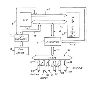
Figure 1 shows the general structure of a computer system
according to the present invention. The system includes a central
processing unit 1 (CPU 1), which is usually a microprocessor, and
which is coupled to memory 2 to permit the CPU 1 to read data from
the memory 2 and write data into the memory 2. The CPU 1 is
coupled to the memory 2 to provide addresses of memory locations
via the processor bus 5, which acts as an address bus and provides
addresses to the memory 2 from the CPU 1. Data (which includes
computer program instructions) from the addressed memory locations
is provided by the memory 2 into the processor bus 6 which acts as
a bidirectional data bus. The CPU 1 may write to the memory 2 by
first providing an address over the processor bus 5 which
addresses memory locations in the memory 2 according to the
address signals over the processor bus 5 and then writing to the
.
memory 2 by providing data over the processor bus 6 to the memory
2. As is well-known, certain signaIs from th~ CPU 1, which may be
carrled over the processor bus 5, indicate whether the CPU 1 is
wr1ting to the memory 2 or reading from the memory 2. The
~ .
.~ .
` ~ ~9~i8~0
l processor bus 5 is a 32-bit address bus and thus includes 32
address lines which provide the address signals. The processor
bus 5 further includes control signals (e.g. R/W (read/write) and
Chip Select) which indicate whether the CPU 1 is reading (from the
memory) or writing (to the memory) and other associated control
signals, including control signals for the particular
microprocessor being used and timing signals (e.g. column address
strobes and row address strobes) as is well-known in the prior art
and therefore is not discussed herein in greater detail. The
processor bus 6 includes a 32-bit data bus (and thus 32 data lines
which provide the data signals) and associated control signals for
the particular microprocessor being used which are typically
included with d~ta buses, as is well-known in the prior art ~e.g.
write enable signal, etc.). The CPU 1 according to the invention
includes an address generation means for generating 232 different
addresses ranging from location $0000 0000 to location $FFFF FFFF
(the dollar sign indicates hexadecimal notation); that address
generation means is typically coupled to the processor bus 5 and
is part oE the CPU 1, such as the microprocessors 68020 (Motorola)
and 80386 (Intel).
The computer system also includes input and output circuitry
which, as is well known in the prior art, is used to interface the
computer to receive data from and provide data to peripheral
units. The details of this circuitry are well known.
Input/output (I/O) circultry 7 is coupled to the ~PU 1 and the
memory 2 via the interconnect bus 13 and the processor bus 6 and
the processor bus -~. The I/O circuitry 7 may be utilized to
provide access to peripheral devices, such as disk drives,
* Trade Mark
, .~
! j.
81t~
1 printers, modems, video displays and other peripheral units for
use with the computer system. As shown in Figure 1, a dis~ drive
8 is coupled to the I/O circuitry by an interconnect bus shown
between the I/O circuitry 7 and the disk drive 8. The I/O
circuitry 7 is coupled to the memory 2 through the processor bus 6
to provide data to the memory and to receive data from the memory
and from the CPU l; the bus 3 allows the CPU to address the
peripheral units attached to the I/O circuitry 7 and allows the
I/O circuitry 7 to address the memory 2. The I/O circuitry 7 is
also coupled tc the CPU to receive data and control signals from
the CPV 1. Thus, the peripheral units, such as the disk drive 8,
can exchange data (which includes programs) with the CPU 1 and the
memory 2; it can also exchange data with any cards and the slots
coupled to the NuBus 10 such as slot 29 which has a distinct
lS number, $9, in the computer system shown in Figure 1.
In a typical transaction the CPU 1 provides an address over
the bus 5. The memory 2, which is coupled to the bus 5, receives
the addresses and provides a value over bus 6 based on the
location addressed according to the address provided on the bus 5.
The data ~rom memory 2 is provided over the processor bus 6 to the
CPU 1. Memory 2 typically includes RAM and may further include
ROM tread only memory). The processor bus 6 is coupled to the
NuBus 10 through the interface 9 and interconnect buses 11 and 12.
The computer system shown in Figure 1 includes six
"expansion" slots which are designed to receive printed circuit
:
board cards and to make electrical connections with circuitry on
the cards, such as caxds SO and 50a in Figures 4 and 14
'.' 11
`, 12g68~
1 respectively. That system includes slots 29, 30, 31, 32, 33 and
3~ which are each coupled to another system bus, NuBus 10, on the
mother board. Thus, slot 29 is coupled to NuBus 10 via the
interconnect bus 19. Each of the slots includes cooperating
terminals, each of which is electrically coupled to a particular
signal line of the NuBus bus 10 through the interconnect buses;
thus, each of the slots 29, 30, 31, 32, 33 and 34 lncludes a set
of cooperating terminals which provide electrical connections to
the NuBus bus 10. A card according to the present invention
includes terminals 51 which are designed to make electrical
connections with the respective cooperating terminals in the slot,
to thereby permit components on the card to receive all of the
signals of the NuBus bus 10
A card in one of the slots 29, 30, 31, 32, 33 or 34 can
; 15 communicate with the memory 2 via the NuBus interface 9, and the
~ CPU 1 can communicate with any memory on the card via the NuBus
; interface 9, which is described below. For example, the NuBus
interface 9 receives addresses for memory on a card in a slot from
the CPU 1 over the bus 25 and provides those addresses onto the
NuBus 10 through interconnect bus 11; the interface 9 serves to
allocate and synchronize the processor buses 5 (through 25) and 6
between the CPU I and any CPU on a card (which may seek to control
the NuBus bus to read from or write to the memoxy on a card).
Similarly, the interface 9 receives addresses for the memory 2
from a CPU on a card ("NuBus device") through NuBus 10 and the
interconnect bus ll; following synchroni~ation to the processor
buses and determination that the NuBus device (which generated the
address) may take control of the processor buses (by placing
,~
12
~Z~613~
1 address signals onto the processor addxess bus 5 through bus 25),
the interface 9 provides the address signals to the bus 25 which
is connected to the memory 2. The memory 2 responds with data
from the addressed location, which data is placed onto the bus 6
which is coupled to the interface 9 which provides that data to
the NuBus device through the NuBus 10.
The computer system shown in Figure 1 utilizes the NuBus bus
as an expansion bus for a computer system on a main circuit board
where the CPU 1 processor buses on the main circuit board may not
be NuBus buses. Thus, the slots coupled to the NuBus 10 provide
the capability to expand the system to include, for example,
additional memory or an additional processor card. ~owever, it is
possible to utilize the invention with a NuBus architecture where
there is no CPU on a main circuit board and no memory on that
board. Such a system is shown in Figure 13 and will be described
below.
Figure 13 shows a general example of the invention for a
computer system utilizing a NuBus bus 120 on a main circuit board
which includes slots each of which is coupled to the NuBus bus
120. The main circuit board of such a system, as illustrated in
Figure 13, may include the NuBus bus 120 and 15 slots designated
as slot 130, slot 131,...through slot 149. Each of the slots is
coupled to the NuBus bus 120 by in interconnect bus; hence, slot
130 is coupled to the NuBus bus 120 by interconnect bus 150, which
interconnect bus normally includes all lines of the NuBus bus 120
and, in addition, includes four lines which serve as distinct
~lndentification line means. These four lines typically carry
:~29681~
. . .
l binary values which together can specify any number from 0 to 15.
Each of the slots receives a distinct identification line means
which provides a different (distinct) number to each of the slots.
That is, a distinct identification line means incorporated as part
5 of the interconnect bus 150 carries a distinct signal equal to 0.
Slot 144 ( slot $E) has a distinct identification line means
incorporated as part OL' the interconnect bus 164 which provides a
value ta distinct signal) equal to $E. It is noted that there is
no 16th slot because the NuBus standard uses the upper most 256-
megabytes ~shown as region 40 in Figure 2) for the small slotspaces (16-megabytes each) allocated to slots 0 through 15. This
is seen more clearly in Figure 2 which illustrates the physical
address memory space of a system such as that shown in Figure 13.
Each of the slots $0 through $E have a "super space" of 256-
megabytes. Thus, for example slot 0 has a super space of 256-
megabytes which was reserved for it from memory location $0000
0000 to $0FFF FFFF. This space is shown generally by number 41 on
Figure 2. This system shown in Flgures 13 and 2 includes a slot
$0 with memory space reserved for that slot; however, because many
microprocessors favor memory in region 91 (the slot $0 super
space), for the sake of convenlence a typical application of the
; general invention (e.g. Figure 13) may not include a slot $0 and
no reservation of memory space 41 will be made for any particular
slot. Thus, any cards in the remaining slots (i.e. slots $1 to
$E) may use the mamory in region 41. Of course, any number of
slots less than 15 may be implemented accor~ing to the invention.
As required by the NuBus standards, each of the slots $0 through
~E have reserved for them 16-megabytes of space located in the
256-megabyte region labelled generally 40; this region spans from
14
.
~:~968~
1 location $F000 0000 to location $FFFF FFFF. Identification
signals, such as the four distinct identification lines are used
to allocate the "small spaces" in the region 40 to each of the
cards. Each of the small spaces in the region 40 is also referred
to in the NuBus standards as the "slot space". Addresses of the
form $FSiXX XXXX reference address space which belongs to the slot
space of the card in slot Si. See pages 30-31 of the IEEE 1196
Specification, Draft 2.0 which is submitted with this disclosure.
Figure 2 illustrates the general physical address memory
space of the system illustrated generally in Figure 13. The main
circuit board which includes NuBus 120 does not include a CPU or
memory. The system clocks 170 on the main cixcuit board pxovide
the NuBus clock signals and are coupled to the NuBus 120 via lines
175 as shown in Figure 13. Not shown, but understood is the power
supply circuitry for the NuBus signals. It is also understood
that the main circuit board of the system shown in Figure 13
should include other NuBus services which are not placed on the
cards, such as the NuBus timeout circuitry.
The computer system shown in Figure 13 would typically
include two printed circuit board cards one of which would be
inserted into one slot and the other card (a second card) being
inserted into another slot. For purposes of illustration, assume
the first card is plugged into the slot $0 (iOe. slot 130) and the
second card is plugged into slot $1 (i.e. slot 131). The cards
are generally illustrated in Figures 4 and 14. They include a
printed circuit board card 50 or 50a and terminals 51, which
terminals are coupled to various components and signal lines on
~29~i8~
1 the card 50 or the card 50a. The terminals 51 are on a portion of
a printed circuit board which protrudes into a receptacle in the
slots which contain cooperating terminals for maklng electrical
connections with respective terminals on the card. The physical-
standards of the interconnections are specified by the NuBus
standard. The cooperating terminals in the slots are coupled to
the various lines and components on the main circuit board; for
example, many of the cooperating terminals in the slots are
electrically coupled to the NuBus bus signal lines. These
cooperating terminals permit the components on the card to receive
the various signals present on the NuBus bus 120 and to permit one
card in one slot to communicate with another card in another slot
through NuBus 120 via the interconnect buses, such as interconnect
150 and 151.
In the present example involving Figure 13, the first card 50
~assumed to be in slot $0) includes a CPU, such as CPU ~1 shown in
Fi~ure 4, and a memory, such as RAM 62 and ROM 62 which are
coupled together through a card bus 65 disposed on the first card
50. The CPU 61 and the memory 62 are coupled to the system bus,
which is the NuBus 120, through the terminals 51 on the card 50.
The second card 50a (see Figure 14) in slot $1 includes a memory
62 shown in Figure 14, such as a random access memory, but does
not include a CPU. Such a card is referred to as a slave card and
cannot take mastership of the bus 120. The second card typically
includes a card bus 65 which includes most (if not all) of the
same signals found on NuBus 120. Certain of the address (and
data) lines of the NuBus 120 (which are referred to as AD (31...0)
in the IEEE 1196 specification, Draft 2.0 since the addresses and
16
. ` ~29~i8~J
1 data are multiplexed over the same lines) are applied to the
decoder means 60. The bus 66 shown in Figure 4 usually carries
the complete NuBus address and data signals and control signals
and power signals. In this disclosure, the 32 address lines of
NuBus (which also serve as the 32 data lines on NuBus) are
referred to as A31 through A0 even through they are the NuBus
signals AD (31...0). Essentially, the decoder means 60 of card
50a permits the memory 62 on the second card 50a to be addressed
when the addresses on the NuBus 120 are in the reserved address
space of the second card, which in this instance is addresses from
location $1000 0000 through location $1FFF FFFF. When the
addresses are in that reserved memory space, the decoder means 60
activates the Chip Select (CS) lines (which are coupled to the
11ne 64 from the decoder means 60) of the memory 62 on the card
50a thereby indicating to the various RAM and ROM chips on that
card that they are being addressed, thereby addressing the memory
62 on the card 50a in slot $1. Thus, the memory on the second
card 50a will receive addresses from the system bus when the
decoder means enables, by the Chip Select pins, the memory chips.
Thus, the CPU on the first card 50 in slot $0, which CPV has
an address generation means for generating 232 different addresses
for addressing memory, provides an address through the terminals
of the card in slot $0 onto NuBus 120. Portions of that address
appear in the decoder means 60 on the second card 50a. If that
25 address is in the range $1000 0000 to $1FFF FFFF the memory on the
second card will respond providing data onto NuBus 120 during the
appropriate timing cycle.
'
~7
l The decoder means 60 on the second card in slot $1 of Figure
13 compares the distinct number of slot $1, which number is $1, to
the most significant hexadecimal digit of the address appearing on
the system bus (NuBus bus 120) to determine when the distinct
number, in hexadecimal, is equal to the most significant
hexadecimal digit of the address. When that occurs, the decoder
means enables the second memory ~o be addresse~ to provide data
onto the system bus. ThUS, the 256-megabyte "super space" is
reversed for ~he second card in slot $1. As explained below, the
decoder means also performs the function of reserving the 16-
megabytes of memory space called for in the specifications of
NuBus systems.
It will be appreciated that slot $1 of Figure 13 is coupled
to a distinct identification line means which provides a distinct
signal to that slot, which signal identifies a distinct number of
that slot. This is true for each of the other slots in Figure 13
(e.g. slot 199 has a distinct signal of $E which is the distinct
number of that slot). Typically, a distinct identification line
means comprises four conductors carrying binary values. For slot
~1, only one of the four lines will carry the binary value 1 while
all others will carry the binary value 0, where the 1 is in the
least significant binary digit. Thus, the distinct identification
line means will provide the distinct signal 1 to the slot $1 which
will identify that slot as having a distinct number $1. It is
understood that other ways of identifying a dlstinct number may be
accomplished, such as providing an identification number which
through arithmetic conversions produces the distinct number of the
18
" 1%~6~3~L0
l slot. Alternatively, one conductor having multilevel logic may be
provided as the distinct identification line means.
A preferred embodiment of the invention utilizing six (6)
slots will now be described with reference generally to Figures 1,
3, 11 and 12. Figure 11 shows a perspective view of a main
circuit board 14 (also referred to as a mother board) which
includes a CPU 1, memory 2 which includes read only memory (ROM),
I/O circuitry 36, and six slots numbered 29 through 3g. The
mother board 14 also includes a connector means for providing a
connection to a key board as shown in Figure 11. As with any
other personal computer system, the mother board 14 also includes
various other circuitry, such as power supplies, latches and
buffers, drivers and may include video circuitry, clock circuitry
and other components typically associated with personal computer
systems as is well known in the prior art. Each of the slots 29,
30, 31, 32, 33, and 39 include cooperating terminals which make
electrical connections with terminals 51 on a card which is
inserted into the slot. Each of the slots 29-34 receive,
according to NuBus standards, substantially all the NuBus signals
in NuBus 10 as shown in Figure 1. The slots receive the NuBus
signals through interconnecting buses 19, 20, 21, 22, 23, and 24
as shown in Fi~ure 1. These connections are commom (identical) to
each of the slots except for the dist~nct identification line
means which identi~ies to each of the slots a distinct number that
each slot has.
In this particular embodiment, slot 29 is assigned a distinct
number $9 by four conductors (lines) carrylng binary values as
.
19
'.
~9~8~
1 illustrated in the table below. These four conductors are part of
the interconnecting bus 19 although they need not be physically
present throughtout the entire length of the lines in the NuBus 10
because they can be locally provided in the immediate proximity of
slot $9. This is similarly true for slots 30, 31, 32, 33 and 34.
The Geographic Address shown in Table 1 is, of course, the
distinct number of each of the slots.
Table 1
NuBus Slot Number~
For Fiquro 1 Sy-~tam
~lot~eographic Bi~ary
Number ~5~a ~L~ ~æ ~iL ~Q Y3~ha~
i~ Fi~. 1
29 $9 GND open open GND1001
$A GND open GND open1010
31 $B GND open GND GND1011
32 $C GND GND open open1100
33 $D GND GND open GND1101
34 $E GND GND GND open1110
~Binary Values shown after logical inversion by an inverter of the
NuBus signals)
Each of the lines in the distinct ldentification line means
for each of the slots is coupled to circuitry which attempts to
pull up the lines to the power supply signal +5V. This circuitry
will usually involve a pull up resistor, according to NuBus
standards, on each of the distinct identification lines, which
resistor will pull up the open signals to substantially ~5V and
the ground signals will remain substantially at ground. The
; circuitry shown in Figure 12, which will be discussed below,
assumes that the open signals have already been pulled up (prior
Y68~
1 to applying them to the decoder means 60) substantially to the
power supply v~ltage level of ~SV and that the NuBus signals
(including the G~3...GA0 signals and address (A31...A0) signals)
have been logically inverted by an inverter. Furthermore, each of
the NuBus signals on NuBus bus 10 must be inverted logically
(through an inverter on the cards) before application to the
circuitry on the NuBus cards ~e.g. card 50 and card 50a);
similarly, signals from the cards onto NuBus bus 10 must be
inverted logically (through an inverter). Typically, these
inverters would be included on the input and output buffers used
on the cards. At the interface 9, which interfaces between the
NuBus bus 10 and the motherboard circuitry (i.e. CPU 1, Memory 2,
I/0 Circuitry 7, the various buses 5, 6, 25, etc.), signals going
onto the NuBus bus 10 are inverted and signals coming from NuBus
bus 10 are inverted. Thus, for example, the GA3 NuBus signal
(GND) which is applied to the slots is inverted to logical one
("1") on the card and is then applied to the circuitry in the
decoder means 60 shown ln Figure 12. These inversions are well
known in the art. Of course, if the CPU 1 and its associated
circuitry and buses (e.g. buses S, 6, 25.) utilize the NuBus
system, standards and signals, then no inversion at the interface
9 is necessary.
It can be seen that in this embodiment (shown in Figures 1,
11 and 3), slot 30 will have the distinct number $A; slot 31 will
have the distinct number $B; slot 32 will have the distinct number
$C in the computer system; the distinct number for slot 33 will be
$D, and slot 34 will have the distinct number $E. In the IEEE's
proposed specificiation for the NuBus, referred to as the IEEE
.
21
1 1196 bus specification the distinct identification llne means are
referred to as the card slot identification and are represented by
the symbol "ID (3...0)" which represent the geographical addresses
GA3, GA2, GA1, and GA0. As noted in that specification of the
IEEE, at page 6, these four lines are not bussed but are binary
encoded at each position to specify the card's position in the
computer.
According to the present invention, a computer system as
generally shown in Figure 1 results in a physical address memory
space as shown in Figure 3 where each of the six slots has a
"super space" containing 256-megabytes of reserved memory space.
Thus, ~or example, slot $9 has a reserved super space beginning at
location $9000 0000 and ending at location $9FFF FFFF. In
addition, slot $9 may also have a small space ("slot space")
reserved according to the NuBus specification; in accordance with
those specifications, slot $9 will have a small space reserved for
it beginning at location SF900 0000 to location $F9FF FFFF. As
shown in Figure 3, the 256-megabyte region 42 contains the small
spaces for the various slots. There is an unreserved NuBus memory
address space 43 which may be used by additional expansion slots
which may be added to a system designed according to the present
invention. The lowest 256-megabyte memory space, designated 45 is
the local address space for the CPU 1 which is assigned the
distinct number $0 as if it were on a card in slot $0. The CPU 1
may be designed to "occupy" additlonal slots--that is it may be
assigned distinct numbers $1, 2 and 3 and the-refore have the
entire region 44 reserved as in the part~cular embodiment shown in
Figure 3; in effect, the motherboard becomes a card in 4 slots
22
1 ~$0, 1, 2, and 3). If the designer seeks to isolate super space
slot $0 completely for CPU 1 J s use ~i.e. prevent a NuBus access to
that super space $0), the NuBus interface 9 will be designed to
prevent such access but permit access to the data in super space
$0 by aliases replicated in super space $1 or $2 or $3. Thus,
NuBus addresses on NuBus 10 in super space $0 may be decoded to
the same respective location (i.e. $0XXX XXXX to $1XXX XXXX) in
super space $1. In such a situation the NuBus cards (in the
actual physical slots $9 through $E) may access the slot $0 super
space by addressing super spaces $1, 2 or 3 which can be designed
to include aliases of the data stored in super space $0. The
address space ($0000 0000 to $1000 0000) is also the local address
memory space for cards operating entirelx on the card without a
NuBus transaction; that is, a card, such as the one shown in
Figure 4 having a CPU may locally address its local RAM on the
card in this same address space 45 provided the CPU does not
initiate a NuBus transaction. Such an arran~ement for purely
local transactions on the card is implemented by address decoders
on the card as is well known in the art.
This particular embodiment shown generally in Figure 1 also
reserves additional memory space for the I/O circuitry and read
only memory (ROM) which is part of the Memory 2 as shown in Figure
3. In particular, address memory space is reserved from $4000
0000 to location $9FFF FFFF. Moreover, memory address space for
I/O operations and circuitry is reserved from location ~5000 OOOO
to location $5FFF FFFF. Figure 3 shows an embodiment of the
present invention where the I/O and ROM memory space is located at
$4000 0000 to $5FFF FFFF. Thus, access to ROM or I/O.information
23
.
96~
l can be obtained by the C~U 1 or by a second CPU 61 by addressing
those locations from $4000 0000 to $5FFF FFFF. Another embodiment
of the present invention is shown in Figure 10 where the
mothexboard I/O and ROM memory space wi~h_L~ectL~2 NuBus cards
is located at $F000 0000 to $FOFF FF~F. In this embodiment, the
memory space of motherboard I/O information and system ROM ~on the
motherboard) which is accessible by the NuBus cards (in NuBus
slots~ is limited to 16 MB (megabytes) while CPU 1 may still
access region $9000 0000 to $5FFF FFFF; however, many possible
systems can be constructed in which this limited space of 16 MB is
sufficient for ROM and I/O use. Thus, for a NuBus card, it may
access the ROM which is part of memory 2 on the motherboard by
presenting addresses in the range $F000 0000 to $FOFF FFFF on the
NuBus bus which causes an access to that ROM. This is implemented
in well-known fashion by the interface 9 which decodes addresses
from NuBus bus in the $F000 0000 to $FOFF FFFF region into the ROM
and I~O region of the motherboard ($9000 0000 to $SFFF FFFF). The
CP~ 1 need not be similarly constrained, and accordingly, it may
seek motherboard ROM or I/O memory by addressing the region
defined by $4000 0000 to $5FFF FFFF; that is, CPU la may have
additional ROM or I/O memory (as part of memory 2) which is not
available to the NuBus cards (which are limited in access to
essential system ROM and I/O on the motherboard). This em~odiment
of the invention, as shown in Figure 10 is consistent with the
NuBus standards which require a configuration RO~ be located at
the top of the 16 MB small (slot) space; thus, slot $0's ROM space
is located at the top of the space $F000 0000 to $FOFF FFFF.
24
2~
l The card according to the present invention will be described
with reference generally to Figures 4, 12 and 14. Figure 4 shows
a card of the present invention which may be incorporated into the
computer system of the present invention by plugging it into one
of the slots of the system, such as slot 29. The card includes a
printed circuit board 50 on which is disposed conducting means
forming various lines such as the card bus 65 and the interconnect
buses 67, 68, and 69. Similarly, Figure 14 shows a card 50a o~
the present invention which is substantially identical to the card
shown in Figure 4 except it does not include a CPU 61 which
; generally permits the card 50 to act as a master with respect to
: the NuBus bus 10 while the card 50a shown in Figure 14 can usually
only be a slave and cannot take control of the NuBus bus 10 and
cannot initiate a NuBus transaction. The cards 50 and 50a include
terminals 51 which make electrical connections with cooperating
terminals in the slots to thereby couple the various components on
the cards to the various slgnals appearing on the main circuit
board 14. All NuBus signals (to and from NuBus) are buffered and
inverted by the buffers 59 on the cards. Thus, for example
interconnect bus 63 connects the address lines A31 through A24 of
the NuBus 10 to the decoder means 60. The bus 63 also includes
power and the distinct identification line means, which in this
embodiment has four signal lines GA3, GA2, GA1~ and GA0, that are
coupled to terminals 52, 53, 54, and 55 respectively. That is,
the signal GA3 is applied to terminal 52 through a cooperating
terminal located ln the slot which receives the card 50.
; Similarly, the signal GA2 is applied to terminal 53; signal GA1 is
applied to ter~inal 54; and GA0 is applied to terminal 55. These
terminals 52, 53, 54, and 55 are coupled to conductor means which
1 present these four signals (as inverted~ to the decoder means 60
at the input 82 of the decoder means 60, as shown in Figure 12.
The signals present in the slots of this particular
embodiment are presented below in Table 2 and are NuBus signals.
Of course, NuBus 10 includes a 32-bit address bus which, during a
first read cycle presents the address of the memory location
sought to be accessed and durinq a second cycle acts as a data bus
and receives data stored in that memory location. During a
writing to memory, NuBus 10 carries, on its 32-bit address bus
during a first cycle, the ~ddress of the location to be written to
and during a second cycle NuBus 10 ~rovides the data to be written
into the location addressed in the first cycle. The NuBus 10 is
substantially an IEEE 1196 bus. The cards generally accept and
use most of these signals although thelr use will depend on the
particular needs of the card and the designer's goals.
Table 2
NuBus Slot Signals De~cription
~i.sa~L p~s~LTj>tiorl,
+SV Power to slot. 5 Volts.
20 +12V Power to slot. 12 Volts.
-12V Power to slot. -12 Volts .
-5.2V Unused in this embodiment. All -5.2V signals are
connected together on the slots.
GND Power return for +5V, +12V, and -12V.
25 RESET Open collector signal. Asserted at power up,
by the CPU 1, or by a push button reset switch
which may be included. Pulled up to +5V by a
lX ohm resistor. Slot card should use this
signal to reset clrcuitry on card.
~6
~g68~
1 SPV Slot Parity Valid. If a card is providing
parity on /SPthis signal is asserted. The
slash ("/") indicates the signal is active
low--that is, it activates its target when
it goes low.
SP Slot Pari~y. Odd parity of /ADO-/AD31 if
/SPV asserted.
;
TMO-TM1 Transaction modifiers. Used during START
cycle to indicate the size of the
transaction. Used during ACK cycle to
indicate completion status.
AO-A31 NuBus Address/Data bits O through 31. Used
during START cycle to indicate address. Used
during ACK cycle to indicate data. NuBus
specifications refer to these sugnals as ADO-
AD31 or AD (31...0) because the same 32 lines
carry address during a first cycle and then
carry data during a second cycle.
PFW Power Fail Warning. An open collector signal
pulled up by a 220 w resistor to +5V. When
- the signal is pulled up the power supply is
activated. Nhen this signal is pulled low the
power supply is disabled. The power supply
itself will pull this signal low as a power
fail warning 2 ms before the AC power is lost.
This is an option under IEEE 1196 standards.
ARBO-ARB3 Arbitration bits O through 3. Open collector
signals which are terminated in the slots in
! accordance with IEEE 1196 specifications ~see,
e.g., Table 6 of the specifications). Used to
arbitrate bus mastership between
the slots according to NuBus Specifications.
GAO-GA3 Geographical Address bits O through 3. Hard
coded binary address of slot. Pins tied to
GND or open (or +5V instead of open).
START Asserted to indicate the presentation of an
address on AO-A31. Also used to start
arbitration for the bus mastership.
ACK Acknowledge. Used to indicate acknowledgement
of START cycle.
RQST Request. Asserted to request bus mastership.
NMRQ Non-master request.~ An open collector signal
which are terminated in the slots in accordance
with IEEE 1196 specifications ~see, e.g., Table
6 of the specifications). Used by card to signal a
;' interrupt to interrupt receiver.
; :
. ~
~. :
~, ~ 27
.. .
~: '
,
9~
1 CLK NuBus Clock. Asymmetrical 10 MHz clock which
sychronizes transactions on NuBus.
The construction and use of the decoder means 60 is known by
those with ordinary skill in the art. It essentially involves the
use of a comparator means with an enabling means where the
comparator compares the NuBus address to the signal appearing on
the distinct line identification means and determines when the
address is wit~in the reserved memory space for the memory 62 of
the card. ~owever, the use of the decoder means in this context
to reserve 256-megabytes of memory space is novel and accordingly,
a description of a simple decoder means including a comparator
means and an enablin~ means will be described. It is within the
; ordinary skill of the art to develop other decoder means which
perform the functions of the present invention.
In a typical transaction between the card 50a and the CPU 1,
the memory 62 is selectively coupled to the CPU 1 through NuBus 10
and lts associated interface 9, described below, to receive
addresses and to provide data (or receive data when written to)
over NuBus 10. The CPU 1 includes an address generation means for
generating 232 different addresses from location $0000 0000 to
location $FFFF FFFF. Addresses from the CPU 1, which are 32-bits
wide, exit the CPU 1 through the processor bus 5. The 32-bit
address then enters the interconnect bus 25 and appears at the
interface 9 whlch determines that the address is within the NuBus
.
address space, which beglns at $6000 00000. Below that address,
~: :
memory 2 and I/O circuitry 7 will be addressed by the CPU 1. At
and above that address, memory in the slot's super spaces or small
:
28
`:
~Z96~
l spaces will be addressed. Interface 9 determines that a NuBus
address is being selected and permits, after synchronizing the
address signals of the CPU 1 to the NuBus and determining
ownership of the NuBus 10 in favor of the CPU 1, the address to
appear on NuBus 10 through the interconnect bus 11. For purposes
of illustration, we shall assume that a card 50a, shown in Figure
14 is in slot $9 which has a distinct number in the system of $9.
The decoder means 60 receives the address signals through NuBus 10
and determines whether the addresses are for that card's memory
~pace.
The decoder means 60 includes a comparator means 70 which
compares the most significant hexadecimal digit of the address
(for reading or writing) to the distinct number, in hexadecimal,
of the slot into which the card having the decoder means 60 is
plugged. The decode.r means also includes a control and clock
signal means 71 which includes NUBUs clock and START and ACK
signals. The decoder means may also further include a driver, a
well-known component in the prior art and hence not shown, which
provides enough current to drive the output from the decoder means
60 to sufficient levels to affect the target of those outputs,
which is the Chip Select (CS) lines and p~ns of the memory 62.
The comparator means 73, which is also part of the decoder means
60, compares the address to determine whether the slot's small
space is being addressed. ~hen one of comparator means (either 70
or 73) determines that the address appearing on NuBus 10 is within
the super space or small space of the card, that particular
comparator means along with the control means 71 activates the
Chip Select (CS) lines connected to the memory 62. The Chip
29
1 Select (sometimes referred to as the Chip Enable Signal) line is
used, as is well known, to indicate to memory, such as memory 62,
that it is being addressed (either for reading or writing). The
Chip Select lines are coupled to li~e 64 as shown in Figures 4 and
14.
The comparator means 70 of the decoder means 60 includes four
exclusive OR gates (''XORI'), such as the exclusive OR gate 76 which
compares the GA3 signal (appearing at input 92) to the most
significant binary bit of the 32-bit address line, A31, which is
input at input 91 of the exclusive OR gate 76. It is understood,
; as noted before, that the NuBus signals in the decoder means 60
are inverted (on the card in buffers 59); thus, GA3...GA0, the
address signals A31...A24 and START, ACK and CLK as used in the
decoder means 60 are inverted. For example, the START signal
shown in Figure 12 is the inverted NuBus START signal. If the
most significant binary bit of the address is equal to the signal
GA3 then a logical 0 will appear at the output of the exclusive OR
gate 76, which output is passed via line 93 to a four input OR
gate 77. The address signals A31 through ~28 and certain signals,
such as power and ground, are applied to the comparator means 70
at the input 83. These signals are then provided to the various
exclusive OR gates of the comparator means 70 as shown in Figure
12. The output from each of the exclusive OR gates in comparator
means 70 will be logical 0 only if the two inputs to a particular
XOR gate are identical. Thus, each exclusive OR gate does a bit
~or bit comparison between one of the bit carrying lines which
acts as a part of the distinct identification line means and one
of the four most significant address lines. It can be seen that
~ - ~0
2~6~:~0 --
1 when a distinct number, in hexadecimal, is equal to the most
significant hexadecimal digit of the address, each of the
exclusive OR gates will produce a logical 0 at its output causing
the output of the OR gate 77 to also be logical 0 causing node 70a
to be logical 0. Node 70a is coupled to the output of OR gate 77
and is also coupled to one of the inputs to NAND gate 90 which is
part of the control means 71. The output from the comparator
means 73 is coupled to node 73a in the control means 71 and is
also coupled to the other input of NAND gate 90. When an address
is in the card's slot space, the output of the comparator means 73
will be logical 0 and node 78 (the output of NAND gate 90) will be
lvgical 1. When an address is in the super space of the slot, the
output of comparator means 70 will be logical 0 and node 78 (the
output of NAND gate 90) will be logi.cal 1. When the address is
not in the slot's small space and not in the card's super small,
node 78 will be logical 0 (since node 70a and node 73a will each
be logical 1). When the address is valid (during a START), the
signal at the output of AND gate ~7 will be logical 1 and will be
clocked ~at the next NuBus clock pulse) to the output Q of the
flip-flop 80 so that a logical 1 appears at node 79. Thus, when
an address is valid ~n~ is in the card's reserved space (small or
super), nodes 78 and 79 will be logical 1 causing line 64 to be
logical 0, thereby activating the memory 62 for addressing. At
the end of the time when the address is valid, the output of AND
gate ~7 will be logical 0 and will be clocked to node 79 (through
the 3K flip-flop 80~ and the memory 62 will be deactivated. When
an adress is valid, START (as shown in Figure 12) is logical one
and ACK is logical 0 (see insert to Figure 12 showing a timing
diagram of the signals START, ACK and CLX which are inputted to
31
96l~
l the means 71). ~he ~CK signal is inverted at the input to AND
gate 87. Thus, when an address is valid, the output of AND gate
87 is logical 1; when an address is invalid, START ls logical 0
; causing the output of AND gate 87 to be logical 0, which value is
clocked to the output Q of flip-flop 80 at the next NuBus clock
pulse as shown in Figure 12. A logical 0 at output Q will
deactivate the CS lines of memory 62. The flip-flop 80 is a
clocked JK flip-flop with the K input tied to the J ("D") input
through an inverter; such a flip-flop is sometimes referred to as
a D-type flip-flop where K is the complement of J. An End of
Cycle signal may optionally be applied to the Reset input of the
flip-flop 80. The signal is obtained from the control circuitry
on the card (e.g. CPU 61~ and it indicates the end of a
transaction. The End of Cycle signal is active low and therefore
it i5 inverted at the input to Reset.
The particular output on line 64 from the control means 71
will depend on whether the memory 62 specifies (according to the
manufacturer) that CS is active low (i.e. at a low voltage like
ground) or high ~+5 volts). In this example, the memory 62 is
assumed to have CS active low ("/CS") and therefore the memory 62
is selected for addressing when the output of means 71 is logical
0. Thus, the activation of line 64 occurs when the output of NAND
gate 72 is logical 0 (low), causing CS to be pulled to
substantially ground and thereby indicating to the memory chips
(memory 62) that they are being addressed.
If there is no match between the distinct number and the most
significant hexadecimal digit of the address, at least one logical
32
1 1 will appear on one of the four outputs of the exclusive OR gates
in the comparator means 70 which causes a 1 to appear at the
output of the OR gate 77, which logical value 1 appears at node
70a. This means the address is not in the card's super space. In
this case, the memory 62 can only be addressed from NuBus 10 only
if the address is in region 42 (small spaces).
The decoder means 60 also includes a comparator means 73
which is responsible for reserving for the particular card a "slot
space" which is in the upper l/16th physical address space of the
system (i.e. region 92 shown in Figure 3). More specifically, a
comparator means 73 allocates 16-megabytes of memory for the card
based on the distinct number of the slot into which the card is
plugged. The comparator means 73 includes a NAND gate 85 which
determines when addresses presented to the card are in the region
92. The exclusive OR ("XOR") gates of the comparator means 73,
such as exclusive OR gate 88, and the OR gate 89 compare the
second most significant hexadecimal digit to the distinct number
of the slot into which the card is plugged to determine when the
distinct number is equal to the second most significant
hexadecimal digit of the address appearing on the 32-bit address
bus of NuBus 10. When this equality condition occurs each of the
XOR gates of means 73, such as gate 88, will produce a logical 0
at its output causing the output of the OR gate 89 to be logical
0. The output of OR gate 89 is one of the inputs to OR gate 75.
The four most significant binary bits of the address (A31...A28~
are applied to the inputs of NAND gate 85; the output of this gate
is logical 0 only when the address is in the small space region
42. The output of NAND gate 85 is one of the inpu~s of OR gate
33
.~ .
~ ~9~ 0
1 75. The inputs to OR gate 75 are both logical 0 only when the
address is in the card's small space in region 42. Thus, the
output of OR gate 75 is only logical 0 when the address is in the
card's small space. The address lines (A27, A26, A25, and A24)
constitute the second most significant hexadecimal digit of the
address appearing on the 32-bit address bus of NuBus 10.
It can be seen that when a card, such as card 50a, is plugged
into a slot having a distinct number $X, a decoder means 60 will
cause that card to have memory space reserved for it from
locations $X000 0000 to $XFFF FFFF and additional memory space
from $FX00 0000 to location $FXFF FFFF.
Transactions between the CPU 1 and NuBus 10 typically require
certain actions of the interface 9 which is referred to as the
NuBus interface 9. The exact implementation of the interface will
depend on the mlcroprocessor selected for CPU 1 and on its
associated buses. In its simplest form, the interface could be
another decoder means, having six decoders, each such as decoder
means 60; that decoder means receives six different distinct
signals having the distinct numbers $0, $1, $2, $3, $4 and $5,
each of those signals for one of the six decoders; this
arrangement would produce the resulting division of physical
address memory space as shown in Figure 3 for the computer system
shown in Figure 1. The interface 9 would also be required to
synchronize any differences in timing between the CPU 1 and the
NuBus CIocks and would determine ownership of the buses being
requested (whether the NuBus 10 or the processor buses 5, 25 and
: 6) by the master device, so that only 1 address appears on all
34
1 buses 10, 5 and 25 at one time. Thus, there would be several
decoder means as shown in Figure 12 each of which receives a
different distinct signal. The output of these decoder means
would be coupled to the CS pins o~ memory 2. At the same time,
the CPV 1 could access the slots attached to NuBus 10 by merely
placing signals on the address bus 5 which is coupled to the
interface 9 which permits the address signal from the CPU 1 to
appear on NuBus 10. Similarly, the CPU 1 could provide data to
NuBus slots by placing the data on the data bus 6 which causes the
data signals to appear at the NuBus interface 9 via the
intexconnect bus 12 and those data signals would then be conveyed
to NuBus 10 and then received by the appropriate slot depending on
the immediately precedin~ address signal which appeared on NuBus
10. In e~fect, the CPU 1 and its associated circuitry including
the memory 2 would appear to NuBus 10 as if it was on a card in
slot 0 or slots 1, 2, and 3. In the following discussion of a
NuBus interface, the term processor bus is generally used to refer
to the data bus 6 which is coupled to the CPU 1 and to the memory
2 and to the address buses 5 and 25 as shown in Figure 1.
The NuBus interface 9, as shown in Figure 5, includes three
state machines and the NuBus clocks which interface between the
six slots (29, 30, 31, 32, 33, and 34) and the NuBus 10 and CPU 1
and memory 2 and their associated circuitry on the mother board
14. In general, the interface 9 must determ~ne ownership of the
re~uested bus(es) between masters, such as CPU l and a CPU on a
card (e.g. CPU 61), to prevent 2 different addresses from 2
different masters from appearing on a bus, such as bus 5 or NuBus
10, simultaneously; that is, the interface 9 must determine bus
6~3~0
1 ownership, via arbitration between possible masters requesting the
same bus, to prevent address collisions on a bus. Similarly,
during data cycles the interface 9 must determine bus ownership,
via arbitration between possible mastexs requesting the same bus,
to prevent dat~ collisions on a bus ~such as bus 6 or NuBus 10).
Moreover, the interface 9 must synchronize the signals of the
requesting master to the timing of the requested bus which will be
driven (for addresses or writing data) or listened to (for reading
data) by the master. The interface may be implemented by well-
known techniques in a programmable logic array.
The signals present on NuBus are described in the 1196specification of the IEEE and in the Texas Instruments'
publications referred to above. Generally, the NuBus standards
specify logical, physical and electrical standards for the four
types of signals present in the NuBus bus 10. These signals
include utility signals such as the clock and the distinct
identification line means; the address/data signals along with
various control slgnals; the arbitration signals; and the power
signals. It can be seen that certain of these NuBus signals
appear on the left side of the Nu~us interface 9 shown in Figure
5. 5ignals provided by the CPU 1 or the memory 2 flow through the
interface or permit the interface to allow the CPU 1 to
communicate with NuBus 10 and vice versa. The following table
descrlbes the signals used ln the NuBus state machlne lnvolved ln
the NuBus interface 9. The particular implementation of the
lnterface 9 will depend on the particular CPU 1 selected for use
on the mother board and on the deslgner's goals.
36
3L~9~ 0
1 Table 3
Signals used in NuBus Stata ~achine~
In N~Bu Inter~ace 9
~L L~
RQST A NuBus signal; active low; indicates a
request for bus mastership.
NVBUS Decoded address from processor CPV 1
indicating an address reference to NuBus;
active low. The address from CPU 1 is
decoded in a decoder means, which can be
readily constructed by one of ordinary
skill in the art, and which determines
when the address on bus 25 in the NuBus
address range of $6000 0000 to $FFFF FFFF.
START NuBus signal; active low; indicates an address
is present on NuBus.
ARB0~ARB3 NuBus signals; active low; arbitration address
of bus masters competing for NuBus mastership.
ACK NuBus "acknowledge"signal; active low; slave
NuBus device is acknowledging START transaction.
RMC Processor CPU 1 signal indicating a
read/modify/ write is occurring on the
processor CPU 1 bus 6 and 25.
AS Processor CPU 1 address strobe indicating the
address lines from the CPU 1 are valid and
a cycle is requested. Active low (~JAS~
/BUSLOCK The processor buses 6, 5 and 25 can not be
interrupted by NuBus transactions into memory 2.
DSACKx The Data Strobe Acknowledge from the memory 2.
3~ BG Processor CPU 1 bus grant indicating the
processor buses 5, 6 and 25 have been granted to
the NuBus to communicate with the memory 2 using
the NuBus to Memory 2~state machine 104.
C16M The processor CPU 1 clock which is used to
qualify signals from the processor CPU 1 as
va
R/n Read/Write signal which is used to indicate
when a read or a write is occurring.
/BR A bus request from NuBus requesting mastership
of the processor buses, principally bus 6
~via bus 12) and buses 5 and 25.
37
~z~
1 /BGACK NuBus signal from NuBus state machine 104
acknowledging granting of the processor buses
by the processor. Typically, NuBus requests
control of the processor buses by issuing a
/BR signal; request for the processor buses
is granted by the signal /BG which is
received by the NuBus to memory 2 state machine 104
which acknowledges receiving the granting of
the processor buses for mastership.
/BERR Bus error signal from NuBus indicatinq there
is an error in the system. This signal is
usually issued by the NuBus timeout state
machine 105 which watches for transactions which
exceed approximately 25 microseconds; any
such transaction is assumed by the bus timeout
state machine to be in error resulting in the
signal /BERR to be sent to the processor.
/DS Datastrobe: ~ NuBus signal indicating the
data lines from the NuBus bus are valid and a
cycle is requested.
The processor CPU 1 typically accesses and requests the NuBus
10 whenever the processor CPU 1 generates a physical address from
$6000 0000 to $FFFF FFFF. The CPU 1 to NuBus state machine 103
determines there is such a request when decoders on the mother
board coupled to bus 25 indicate an address on bus 25 has a most
significant hexadecimal digit between $6 and $F, including $6 and
$F. Under these circumstances~ the output of those decoders
causes the assertion of the /NUBUS signal. The state machine 103
then synchronizes the request for NuBus control with the NuBus
~30 clock and presents the same address over the bus 10 ~f~
determlning;the CPU 1 may take ownership of NuBus 10 to drive the
address signals onto the NuBus 10. If a card on NuBus responds,
the data is transferred. If no card responds, a NuBus timeout
occurs and a bus error (/BERR) is sent to the processor, which
~ :
usually causes execution of an error handling routine. The NuBus
timeout state machine 105 monitors the time between START signals
;
38
~Z~6~L0
1 on NuBus and acknowledge (ACK) signals on NuBus. When the time
between those signals exceeds 255 NuBus Clocks, according to the
NuBus standards, the NuBus timeout state machine generates the bus
error as indicated above. Figure 8 illustrates the signals
involved in the processor CPU 1 to NuBus transaction through the
NuBus interface 9 and more specifically through the processor to
NuBus state machine 103. The signals on the right side of the
block 103 shown in Figure 8 which are directed to the CPU 1 side
of machine 103 are NuBus signals. The right side of machine 103
is the NuBus side of the system and includes the 6 slots. On the
left side of the interface 9 is the CPU 1 and memory 2 portion of
the system. This is also true for Figure 9. Signals entering
(i.e. the arrow is directed towards the machine 103) the machine
103 from the NuBus side are generally NuBus signals and signals
exiting the machine 103 on the NuBus side are generated by the CPU
1 or the result of the interaction CPU 1 and the machine 103.
Slmilarly, signals on the CPU 1 side of the machine 103 which
enter the machine 103 are signals generally from the CPU 1 or
memory 2 or circuitry associated with that portion of the system.
The signals on the CPU 1 side of machines 103 and 109 are carried
by the bus 12 of Figure 1 and the signals on the NuBus side of
machines 103 and 104 are carried by bus 11.
The normal CPU 1 to NuBus transaction starts with the state
machine 103 waiting for the signal /NuBus to be asserted (which is
synchronized to the 10-MHz NuBus clock). When this signal is
asserted, and no other bus masters are asserting RQST on NuBus 10,
state B is entered into from state A, the prior waiting state.
State B has asserted the RQST signal of NuBus and establishes a
39
1 request by CPU 1 for the NuBus 10 among any other bus masters
which are asserting RQST at the same time. For purposes of
arbitration under the NuBus standards, the CPU 1 is assigned to
slot $0.
State B is followed by state C during which the arbitration
and acknowledge (ACK) signals are sampled to check if any other
NuBus transaction is in progress or if some other Nu~us master has
won NuBus 10. If a transaction is in progres~ and no other bus
master won mastership, state C is retained. If any other bus
master requested the bus during state B, state D is entered into.
[Note: Since the processor CPU 1 accesses the bus from slot $0,
it always loses to the other slots since the arbitration is based
on the distinct number under the NuBus standard] If no other
master has won the bus and no other transaction is occuring, state
E is entered into.
State ~ asserts the START si~nal of the NuBus bus 10 and
drives the address from CPU 1 onto the NuBus 10. It is understood
that lat~hes and buffers are used to temporarily store addresses
and data in these state machines 103 and 104 and generally in the
system. State F follows State E and waits for the acknowledge
signal (ACK) from the card which was addressed. When the
acknowledge signal is asserted on NuBus 10, and no other masters
are requesting the bus 10, a State G is entered in which the
DSACKx signals to the processor CPU 1 are ~enerated to finish the
process cycle. If no other master is asserting RQST during State
G, State H is entered into which is a State in which the NuBus 10
ls "parked" which is to say that a second NuBus transaction from
.
1 the processor CPU 1 will be able to go directly to state E to
start the NuBus access instead of state A. If RQST is asserted
during States F, G, or H, the NuBus 10 must be rearbitrated to
determine the current bus master and State A becomes the waiting
State rather than State H. These sequences of states may be
executed by well known state machine techniques. The following
table summarizes the states and signals involved in the processor
CPU 1 to NuBus interface which is executed by the CPU 1 to NuBus
state machine 103.
Table 4
Proceq~os CPU 1 to NuBus State-~
Signals
5~ UIl~ i Deac~i~tion
A Idle state. Waiting for
the processor CPU 1 to
generate NuBus address
access (addressing a
memory locatlon from
$6000 0000 to $FFFE~ FFFF)
and for RQST ~from cards)
to be deasserted by cards in
the NuBus slots.
B RQST Request NuBus. The
processor CPU 1 is
requesting NuBus bus and
no other RQST asserted.
C RQST Test for arbitration win.
The arbitration lines
should all be deasserted
since processor CPU 1 is
arbitration number zero.
If last cycle is waiting
for ACK, stay put. If an
arbitration line is
asserted, try again after
next START transac~ion.
D RQST Wait for next round of
arbitration. START
indicates next round of
arbitration is available.
41
~z9~
1 E START, AO-A31 Start transaction.
~NuBus) Assert processor CPU 1 address
on 32-bit address line of
NuBus 10.
F AO-A31 Wait for ACK. Wait for
acknowledge from slave
device. CPU 1 Asserts AO-A31
~NuBus) if CPU 1 is writing to
NuBus device (e.g. a card).
Note whether RQST is asserted
to determine if bus will
remain "parked". If RQST
is asserted, the state
machine will recycle to
state A after state G.
G DSACKO, DSACKl Assert DSACKx. NuBus
slave completed trans-
action, and processor
CPU 1 cycle. NuBus
remains "parked".
H Wait for next processor
CPU 1 to NuBus trans-
action. NuBus remains
"parked" to allow quick start
to next cycle.
The state machine shown in Figure 8 receives the address
signals of the CPU 1 ~AO-A31) from the CPU 1 on the bus 25. The
slgnals appearing on the right side of the state machine 103 are
NuBus signals. Certain signals on the left side of state machine
103 are also NuBus signals such as the clock signals /CNlOM and
C20M, as well as /NuBus although the latter is caused by CPU 1 by
generating a NuBus address.
The NuBas to CPU 1 buses state machine 104, as shown in
Figure 9, is for accesses for the memory 2 (which may include RAM,
ROM and I/O) from NuBus. In one embodiment, if an address from
$0000 0000 to $5FFF FFFF is presented on the NuBus, then the NuBus
to processor buses state machine 104 requests the processor buses
~ from the CPU 1 and performs an access to the address. An
:
42
` ~296~3~0
~ .
1 alternative embodiment ~Figure 10) will also be described in which
accesses to RAM of memory 2 occur by addressing $0000 0000 to
$3FFF FFFF and accesses to ROM or I/O of the motherboard occur by
addressing $FOOO 0000 to $FOFF FFFF. Normally, after the data is
sent to or from the NuBus master (i.e. the card in the NuBus
slot), control of the processor buses 5 and 6 is returned to the
processor CPU 1.
The following Table describes the states and signals involved
in the NuBus to CPU 1 buses transaction.
Table 5
Signals
~er~U~ ~suu~ci5
i
A1 Idle state. Waiting for address on
NuBus 10 to processor buses
locations ~e.g. $0000 0000 to $3FFF
FFFF and $FOOO 0000 to $FOFF FFFF).
If the processor buses are not
locked (e.g. by locking the
processor buses through assertion of
Buslock signal of CPU 1) and the CPU
1 is not doing a NuBus access, the
; processor buses will be requested.
If Buslock is asserted, then NuBus
access to Memory 2 is delayed until
Buslock is reasserted and the state
remains at A1.
B1 BR Bus Request asserted. Request by
NuBus of processor buses for NuBus
to Memory 2 transaction. Wait for
; 30 CPU 1 to assert Bus Grant and
deassert address strobe.
C1 BGACK, AO-A31 Assert mastership of processor
(on bus 25) buses and set up addresses and/or
data
DO-D~l
(on bus 6)
R/W
43
~9~10
l D1 AS; DS; AO~A31 Address strobe asserted.
(on bus 25) Data strobe asserted.
E1 DO-D31 ~ait for valid data from Memory 2
DSACK (or write to Memory 2 during time
when data is valid).
Wait for Data Strobe Acknowledge
(DSACK) from Memory 2 to indicate
end of cycle.
F1 ACK (NuBus) MuBus to processor buses
transaction complete. Wait to
; determine if next cycle will
continue with NuBus controlling the
processor buses. NuBus can loc~
onto the processor buses by
asserting a Lock Attention signal
which causes CPU 1 to relinquish
control of the processor buses for
several transactions without CPU 1
contention until Null Attention
signal is asserted; assertion of
Lock Attention causes looping of the
states B1 to F1.
The NuBus to CPU 1 buses transaction begins with state A1
shown in Table 5 above, where the state machine 104 is idling by
waiting for an address on NuBus 10 in the Memory 2 memory space
(e.g. $0000 0000 to $5FFF FFFF; or, in the alternative embodiment
of Figure 10, $0000 0000 to $3FFF FFFF and $FOOO 0000 to $FOFF
FFFF). NuBus accesses to the processor buses can be prevented by
asserting the Buslock signal which causes all NuBus transactions
to this address space to be acknowledged with a "try again later"
response. If the address is within the Memory 2 space and Buslock
is not asserted, then state B1 is entered.
At state B1, the CPU 1 releases the processor buses by
issuing a BusGrant which responds to a Bus Re~uest; the Bus Grant
is acknowledged by the NuBus device by a BusGrant Acknowledgement
in the next state, Cl. The addresses are driven onto the
~.
~ 44
.. ` ~2~6~
1 processor address buses and the data is transferred ln states D1
and El. The transaction is completed in Fl when the NuBus ACK
signal is asserted on NuBus 10.
In the alternative embodiment of Figure 10, the NuBus devices
access the RAM of memory 2 by presenting addresses in the range
$0000 0000 to $3FFF FFFF. NuBus devices, in this embodiment,
access a portion of the motherboard's ROM memory space and a
portion of the motherboard's I/O memory space (which is usually
physical RAM set aside for I/O use) indirectly by presenting
addresses on NuBus 10 in the range of $F000 0000 to $FOFF FFFF
(slot space $0). In this embodiment, addresses on NuBus 10 in the
range $4000 0000 to $5FFF FFFF do not access ROM or I/O, but
addresses on the CPU 1 buses (e.g. bus 5) in that range do access
the complete motherboard ROM and I/O memory space. In keeping
with NuBus standards, the portion of ROM of the motherboard (which
is assigned to at least slot $0) which is accessible to NuBus is
placed at the top of the slot space $0. The partlcular allocation
of the memory in slot space $0 between motherboard ROM and
motherboard I/O depends on the designers needs. In one preferred
embodiment, the slot space $0 is divided in half such that an
address to $F080 0000 to $FOFF FFFF on NuBus 10 produces an access
to an 8 me~abyte region of the ROM of the motherboard (i.e. ROM of
the memory 2), and an address to $F000 0000 to $F07F FFFF on NuBus
10 produces an access to an 8 MB (megabyte) region of the I/O
memory space. The particular 8 MB portions of ROM and I/O memory
space will depend on what regions of memory NuBus deYices will
need or want to use. Often, the entire system (motherboard) ROM
and motherboard I/O will fit into the 16 MB region of slot space
6~0
1 $0. Well known decoders may be used to cause the decoding from
the NuBus address in slot space $0 to the appropriate ROM and I/O
locatlon.
:
: :
: ~ 46