Note: Descriptions are shown in the official language in which they were submitted.
~%9~
-1- PCT-19074
5~ r~~
- ALUMINUM ALLOY ~h~CQ~DU~ PACKAGES
This invention relates to semiconductor
packages in general and, more particularly, to
light weight non-hermetic packages having
improved corrosion resistance.
In the electronics industry, the rapid
development and extensive use of integrated
circuits, such as silicon based semiconductor
lQ devices have resulted in a proliferation af
package designs to house electronic devic~s.
The packages may be broadly cateyorized a~
either hermetic or non-hermetic.
Hermetic packages are generally formed from
ceramic or metal components and are usually
glass sealed. An example of a hermetic package
is the CERDIP, ceramic dual in-line package.
Non-hermetic packages are generally formed
from ceramic, metal or plastic components and
2~ are usually epoxy sealed. Non-hermetic packages
are also formed by molding a plastic body about
the electronic device.
Metal non-hermetic packages comprise metal
bas0 and cover componen~s with or without a
window frame. ~ lPadframe is disposed either
between the base component and the cover
component or between the base component and the
window frame. The package components are bonded
together with a polymer adhesive such as epoxy.
3~ ~ Epoxy sealed non-hermetic packages are
disclosed in U.S. Patent No. 4,105,861 issued to
Hascoe and U.S. Patent~No. 4,594,770 issu d to
B~tt. Copper or a copper alloy is preferred in
U.S. Patent No. ~,594,770 due to the high
thermal conductivity of~the metal.
.
~LZ~681S
-2- PCT-19074
It is desirable to maximize the strength of
the epoxy to metal bond. One method of
improving the adhesive to metal bond is to coat
the metal components with a second material
which forms a stronger bond to the metal
substrateO The second material may be deposited
by cladding, platiny, sputtering, vapor
deposition or any other technique known in the
art. The bond may be further strengthened by a
post deposition treatment such as oxidation or
passivation. Coating of a copper based
leadfram to improve resin adhesion is disclosed
in U.S. Patent No. 4,707,724 issued to Suzuki et
al.
A molded plastic package has insufficient
thermal conductivity for high power circuits
which generate a large quantity of heat during
operation. Copper base and cover components may
add too much weight for applications such as
2P aerospace.
An aluminum based metal package would have
a significant advantage over copper based metal
packaqes. The weight of the assembled package
is up to about 60% less than that of the
comparable copper package. Weight is important
in aerospace, military and outer space
applications where a large number of electronic
devices are utiliæed and a significant weight
penalty exists.
3~ Until now, aluminum and aluminum alloys
have not been satisfactory for electronic
packages due to the tendency of the metal to
corrode. The assembled packages fail a salt
spray corrosion test specified in
Military-Standard-883.
-3- PCT-19074
The salt corrosion test comprises an
aqueous solution containing 3% by weight sodium
chloride. The solution is held at 350C and the
packages are immersed for 24 hours. Upon
removal, the packages made from an alumin~um
based alloy exhibit numerous small corrosian
pits. By comparison, a package made using
copper alloy 197 having a nominal composition of
0.5% Fe, 0.035% Mg, 0.18% P and the balance
copper exhibits no corrosion pitting a~ter the
same 24 hour salt corrosion test.
: It is an object of the present invention to
manufacture an electronic package from aluminum
or aluminum based alloy components.
It is an advantage of the present invention
that the aluminum or aluminum based alloy
components have improved corrosion resistance.
It is a feature of the invention that the
improved corrosion resistance is imparted by
anodizing at least a portion of the aluminum or
aluminum based alloy components prior to
bonding.
It is an advantaye of the invention that
aluminum or aluminum based alloy package
components weigh up to about 60% less than
comparable copper or copper alloy components.
It is an advantage~of ~he invention that
: the aluminum or aluminum based alloy components
:are less costly than comparable copper or
: 3~ copper alloy based components.
It is an advantage of the invention that
the electronic device may be electrically
: isolated from the package components while high
thermal conductivity is maintained.
In accordance with the invention, the
i8~5
,, .~
-- 4 --
foregoing objects, features and advantages are
obtained by a package for encasing an electronic
device, characterized by:
an aluminum or aluminum alloy base
5 componenti
an aluminum or aluminum alloy cover
component;
said base component and said cover
component defining a cavity;
a leadframe disposed between and adapted
to be bonded to said base component and to said
cover component; and
an anodization layer covering at least
that portion of said base and cover components
exposed to the atmosphere.
In accordance with a further embodiment of
the invent.io~ there is provided a package for
encasing an electronic device, characterized by:
an aluminum or aluminum alloy base
component;
a window frame component having first and
second surfaces; ,
a leadframe disposed between and adapted
to be bonded to said base component and to the first
2s surface of said window frame componenti
a cover component adapted to be bonded to
the second surface of said window frame component;
and
an anodization layer covering at least
that portion of said base and cover components
exposed to the atmosphere.
~ ~ From a different aspect, and in accordance
; ~ with an embodiment of the invention, there is
provided a process for assembling a package for
s encasing an electronic device characterized by the
steps of:
. . ~ ~ ' , ,
.
- 4a -
providing a base component and a cover
component, said base and cover components comprised
of aluminum or an aluminum based alloy;
anodizing at least that portion of the
5 surfaces of said base and cover components exposed
to the atmosphere;
disposing a leadframe between said base
component and said cover component; and
bonding said leadframe to said base
10 component and to said cover component subsequent to
connecting said electronic device to said base
component and to said leadframe.
In accordance with a still further aspect,
an embodiment of the invention comprises a kit for
the assembly of an adhesively sealed package
designed to encase an electronic device,
characterized by:
- a metallic base component selected from
the group consisting of aluminum and aluminum based
alloys, said base component having a first surface
` an and opposing second surface, said first surface
having at least selected portions thereof coated
with an anodization layer having a thickness of from
about .25 microns to about 50 microns (lO to 2000
2s micro-inches) for receiving a polymeric adhesive;
and
a metallic cover component selected from
the group consisting of aluminum and aluminum based
alloys, said cover component having a bonding
surface for bonding to the first surface of said
base:component and an opposing surface, said bonding
surface having an outer ring portion and an inner
depressed portion bordered:by said ring portion,
: said ring portion coated with an anodization layer
havlng a thlckness of from about .25 microns to
.
; ~ :
.: '
' '`
~ .
.
~G~
- 4b -
about 50 microns (lO to 2000 micro-inches) for
receiving a polymeric adhesive.
In accordance with a further embodiment of
the invention there is provided a kit for assembly
s of an adhesively sealed package designed to encase
an electronic device, characterized by:
a metallic base component selected from
the group consisting of aluminum and aluminum base
alloys, said base component having a first surface
10 and an opposing second surface, said first surface
having at least selected portions thereof adapted to
receive a polymeric adhesive by coating with an
anodization layer;
a metallic cov~r component selected from
the group consisting of aluminum and alum-num base
alloys, said metallic cover component having a
bonding surface for bonding to the first surface of
a window frame component and an opposing surface,
said bonding swrface having an outer ring portion
and an inner portion bordered by said ring portion,
said ring portion adapted to receive a polymeric
adhesive and coated with an anodization layer; and
said window frame component selected from
the group consisting of aluminum and aluminum base
2s alloys having an anodization layer coating all
surfaces and edges, said surfaces adapted to receive
a polymeric adhesive.
Accordingly, a light weight non-hermetic
package comprising aluminum or aluminum based alloy
components is claimed. Improved corrosion
resistance is obtained by an anodization surface
applied to at least a portion of the surfaces of the
package components.
It is known to form a refractory oxide
3s such as aluminum oxide on the sealing surface of the
alloy to enhance bonding. For example, U.S. Patent
:- ~
\
- 4c -
No. 4,542,259 issued to Butt discloses forming a
refractory aluminum oxide coating on copper alloy
CDA 63800 to enhance glass sealability. Copper
alloy 63800 is a copper based alloy containing from
about 2% to about 12% aluminum.
An anodized aluminum surface differs
compositionally from a refractory aluminum oxide
surface. The refractory oxide is anhydrous, or
water free. The anodized surface comprises hydrated
10 aluminum oxide The water concentration varies from
a trace up to about equal molar concentration with
the aluminum oxide (A12O3 H2O). The anodization is
deposited by an electrochemical process rather than
high
, ~ ~
~ \; ~ '.ii :
:b
.' ' .' ' " ' ~ ,~, .
-5- PCT-19074
temperature oxidation as usually used to form
refractory oxide layers.
Unlike chemical deposition techniques such
as plating, sputtering or vapor deposition,
anodization is a chemical conYersion process. A
chemical conversion process forms a surface
coating consisting of a compound of the base
metal.
A better under~tanding of the essential
lC features of the invention will be obtained from
the following specification and accompanying
drawings.
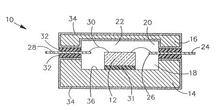
FIG. 1 illustrates an electronic package
manufactured according to the invention.
FIG. 2 illustrates a window frame type
electronic package manufactured according to the
invention.
FIG. 1 illustrates an electronic package 10
adapted to house an electronic device 12. The
electronic device 12 is typically an integrated
circuit such as a silicon based semiconductor
device. The package 10 is comprised of a base
component 14 and a cover component 16. A
depression 13 is optionally formed in the base
component 14. A second depression 20 is
optionally formed in the cover component 16.
These depressions serve to form a cavity 22 to
encase the~electronic device 12. The
depressions are usually formed by milling or
chemical etching,: Alternatively, a metal
deformation process may be used to form the
cavities.
rhe base component 14~ and the cover
.
~68~S
-6- PCT-19074
component 16 are preferably manufactured from
aluminum or an aluminum alloy. Aluminum alloys
designated by the ASM (American Society for
Metals) as 3xxx series are preferred. These
alloys contain up to about 1.5% by weight
manganese along with other alloying elements.
The alloys have good thermal conductivity and
about 20% higher strength than the alloys
de~ignated as the lxxx series (greater than
1~ 99.00% aluminum). A most preferred aluminum
alloy is aluminum alloy 3003 having a nominal
composition of about 0.12% by weight coppex,
about 1.2% by weight manganese and the halance
aluminum.
A leadframe 24 is disposed between the base
component 14 and the cover component 16. The
leadframe 24 comprises inner lead ends 26 and
outer lead ends 28. Inner lead ends 26 are
adapted for electrical interconnection to the
electronic device 12 as by wire bonds 30. The
outer lead ends ~8 are adapted for connection to
an external device such as a printed circuit
board.
The eleotronic device 12 is bonded to the
ba~e component 14 by a die attach 31. The die
attach 31 may be electrically conductive or
electrically insulating dependent upon the needs
of the electronic device 12. As the
coe~ficient of thermal expansion of the
aluminum or aluminum alloy base component 14 is
3 from about 230 x lO 7 ~C to about 274
lO 7 /~C and the coefficient of thermal
e~pansion of the electronic device is about
49 ~ lO 7 /C, it is preferred to use a
compliant die attach system. A compliant die
~Z9~;8~5
-7- PCT-19074
attach system will absorb the strPsses created
by the coefficient of thermal expansion mismatch
generated durinq die a~tach, package sealing and
device operation. Silver filled polyimide die
attach systems are particularly well suited ~or
the package as are die attach systems
incorporating a relatively low coefficient o~
thermal expansion buf f er.
Sealing the leadframe 24 to the base
component 14 and the cover component 16 are
honding layers 3~. The bonding layers may be
any adhesive known in the art and are commonly
a polymer adhesive or a sealing glass.
While the invention is applicable to both
glass sealed and polymer sealed packages, it is
more particularly drawn to polymer sealed
packages and will be described in that context.
The adhesive layers 32 may be comprised of
any suitable thermosetting or thermoplastic
resin. A resin adhe~iv~ such as an epoxy, for
example, Ablestik 550K manufactured by Ablestik
Laboratories of Gardena, California is one
exemplary bonding material. This sealant is
bonded at a temperature in the ranye of from
about 145C to about 155C. Bonding times range
from about 1 hour to about 2 hours.
It has been discovered that an anodization
layer~34 on at leas~ a portion of the base 14
and cover 16 components yields superior results.
Both a thin anodization layer, de~ined as having
a thickness of less than about 2.5 microns
(100 microinches) and a thick anodization
layer produce aluminum base electronic
packages which e~hibited no corrosion when
subjected to the 24 hour salt corrosion
test. The preferred thickness of the
~ ~Z9~8~S
-8- PCT-19074
anodization layer is from about 0.25 microns (10
microinches) to about 50 microns (2000 micro-
inches). The most preferred thickness is in the
range of from about 1.25 microns (50 microinches)
to about 5 micron~ (200 microinches).
The anodiza~ion layer may be applied by any
technique known in the art. For example, an
aqueous solutivn containing about 28 volume
percent sulfuric acid at a temperature of about
20C deposits a satisfactory anodized layer on
the sur~ace of an anodically charged aluminum or
aluminum alloy substxate. The anodization layer
is applied either before or after the formation
of depressions 18, 20 in the base 14 and cover
16 components. ~he sur~ace 36 of the depression
may either be anodized or bare metal.
A sealing process is preferably used to
reduce porosity. A typical anodization sealing
process is water or steam sealing. The process
entails exposing the anodized surface to
pressurized steam for from about 30 minutes to
about 60 minutes. The anodized surface hydxates
to form crystalline boehmite (A1203H20). The
conversion to boehmite results in a volume
increase e~fectively closing any pores in the
anodized surface. Other satisfactory sealing
solutions include nickel acetate, ferric
oxalate, dichromates and molybdates.
A slight thermal conductivity advantage is
achieved with bare metal, without an anodization
layer. The bare metal is electrically
conductive. For certain electronic
applica~ions, such as housing a bipolar device,
a conductive substrate is not desirable. These
devices are preferable electrically isolated
from the package and the us~ of a thermally and
29613~;
-9- PCT-19074
electrically conductive die attach such as
silver filled epoxy on bare metal results in
shorting. The present invention overcomes this
problem by disposing a dielectric layer of
anodization between the conductive die attach
and the base metal electrically isolating the
device from the package.
Even though the thermal conductivity of
aluminum alloy 3003 is only about 50% that of
1~ copper alloy 197, the eJC values are about equal
and the ~JA value only in the range of ahout
from 10% to about 15~ higher. It is believed
the reason for this is that the largest
contributor to eJC and eJ~ values is the die
attach material. The thermal resistance of the
aluminum substrates is a minor contributor to
the e values.
As discussed hereinabove, an advantage of
metal packages over ceramic or plastic pac~ages
2~ is thermal performance. Thermal performance is
typically recorded as eJC and eJA. eJC is a
measure of the temperature di~ference between
the junction and the case. The junction
temperature is measured at the die attach 31 and
the case temperature is measured at a point
along the package base 14. Similarly, eJA is a
measure of the temperature difference between
the junction and the ambient environment. Table
1 gives measured values for a 48 pin dual in
3~ line epoxy sealed package havin~ either copper
alloy 197 or aluminum alloy 3003 componenets.
Z968:~5
-10- PCT-19074
TABLE 1
Component eJC eJA
Composition C/W stillforced
air C/W air C/W
Cu alloy 1~72 - 3 18.5 - 225 - 6
Al alloy 3003 2 - 3 17 - 19 8
Copper has a density about three times that
of aluminum. A package weighing about 60% less
1~ than a conventional copper metal package may be
obtained with only a minimal loss in thermal
performance in accordance with this invention.
The invention is not limited to dual in
line packages. QUAD packages having lead ends
approaching the electronic device from all four
sides of the device periphery may also be
assembled using aluminum based components having
anodized surfaces.
Window frame packages as shown in FIG. 2
2~ are also made according to the invention. A
window frame package 50 is similar to the above
described package with the exception that a
window frame 52 is disposed between the
leadframe 24 and the cover component 16'. A
window frame package is desirakle in the
situation where the electronic device 12 is to
~e die attached and wire konded at a different
time than the package is assembled as where a
vendor manufacturers the package for ~hipment to
3~ a device maker.
The window frame 52 is comprised of any
somewhat rigid material which is ~ondable to
sealant 32. The window frame preferably has a
coefficlent o~ thermal expansion close to that
39 of the cover component l6' or the leadframe 24.
~Z968~
-11- PCT-19074
Preferred window frame materials are copper,
aluminum and the alloys of the metals. To
minimize packa~e weight, aluminum or aluminum
alloys are most preferred. For improved
strength, manganese containing aluminum alloys
such as aluminum alloy 3003 are preferred.
In the window frame package, a leadframe 24
is disposed between the window ~rame 52 and a
base component 14. For improved corrosion
1~ resistance, an anodization layer 34 is applied
to the base component 14 and the window frame
component 52. The leadframe 24 is bonded to a
first side of the window frame 52 and to the
base component 14 with a suitable bonding agent
32 such as a glass or a polymer adhesive.
Subsequent to bonding the leadframe 24, the
electronic device 12 is bonded as by a die
attach 31 and electrically connected to the
inner leads 26 of the leadframe 24 by wire bonds
2Q 30. ~ cover component 16 is then~ bonded to the
second side of the window frame 52 with a
sealant 56 to encase the electronic device 12.
The sealant 56 is selected to be any
makerial known in the art which will bond to the
window frame 52 and the covor component 16 at a
relatively low temperature. The desired bonding
temperature is low ~enough so as not to degrade
the sealant 32 or the electronic device 12. The
sealant preferably bonds; at a~temperature of
less than about 150C. The sealant may ~e any
compatible thermosetting or thermoplastic
adhesive. A;prefe~red sealant is the epoxy
Ablestik 550.
It is preferable to coat the cover
component 16 with an anodlzation layer 34 for
.
~z9~
-12- PCT-19074
improved corrosion resistance. The anodization
layer may be applied over all or a portion of
the bas~ component 14, the cover component 16
and the window frame 52. It may not be
desirable or necessary to entirely coat every
sur~ace of the base and cover component.
The reyion of the surfaces coated varies.
At a minimum,- all surfaces exposed to the
atmosphere should be cvated to prevent
lQ corrosion. The seal areas, those surfaces in
contact with the sealants 32 and 54 may be
coated for improved bond strength. The
remaining surface areas are optionally coated
de~endent upon desired electrical, thermal and
moisture getting properties.
Interior surfaces 36 and 54 may preferably
not be anodized. ~etter thermal conductivity is
achieved by bonding the electronic device 12
directly to the aluminum or aluminum alloy
2~ surface 3~. IP the sur~ace to be bonded 36 is
not anodized, the electronic device may be
electrically connected to the base component as
for grounding. If the sur~ace 36 is anodized,
the electronic device may be electrically
isolated from the package.
A moisture trapping surface, such as a
gettar alloy may be formed on the interior
surface 54 o~ the cover component to trap
residual moisture and sealing reaction
3~ by-products.
Surfaces free of anodization may be
prepared by a variety o~ methods. The portion
of the surface desired to be anodization free
may be coated with a chemical resist or a
plater's tape prior to immersion in the
~29~
-13- PCT-19074
anodizing 501ution. The entire surface may be
anodized and the desired region made anode free
by a mechanical operation. For example, a
milling step is useful to form the base
depression 18.
By varying the anodization parameters, a
roughened anodization layer may be formed. A
rougher surface finish increases mechanical
locking of the bonding component, particularly a
1~ polymer sealant, and improves the bond strength.
It is apparent the invention provides ~n
electronic package having improved
characteristics. The package is more light
weight than copper based packages and has better
thermal conductivity than plastic based
packages. Anodizing at least a portion of the
aluminum surfaces provides for increased
resistance to corrosion and further increases
bond strength.
A pressure pot test was used to evaluate
the strength of the adhesive bond to anodized
aluminum alloy based package6~ The packages
were epoxy sealed and th~n subjected to 100~
relative humidity at 121C and 984 gm/cm2 (14
psi). Leak testing revealed no adhesive
failures afte~ 200 hours.
By adjusting the chemical composition and
operating parameters of the anodization and
sealing solu~ions, different color surfaces may
be obtained. This is beneficial in consumer
electronic applications where a black or gold
~inish is often desirable.
It is apparent that there has been provided
in accordance with this invention a number of
embodiments which are especially suited for
`` ~L29~81~
-14- PCT-19074
electronic packages comprised of aluminum or
aluminum alloy components which have improved
resistance to corrosion. While the invention
has been described in connection with the
embodiments thereof, it i5 evident that many
alternatives, modifications and variations will
be apparent to those skilled in the art in light
of the foregoing description. Accordingly, it
is intended to embrace all such alternatives,
1~ modifications and variation as fall within the
spirit and broad scope of the appended claims.
3~:
.