Note: Descriptions are shown in the official language in which they were submitted.
1296~19
STANF.7lA
DISTRIBUTED SENSOR ARRA~ AND HETHOD
- USINC A PULSED SIGNAL SOURCE
~ackground Or the In~ention
The present invention relates to riber-optic sensors,
and particularly to distributed riber-optic sensor arrays
~hich utilize time di~ision multiplexing in their
¦ operation.
Over the past re~ years, riber-optlc devices have
10 1 been actively studied and developed rOr u~e in various
sensing applications ln a uide range of rields. One
reason ror this interest is the sensitiYity Or optical
ribers to envlronmental conditions ~hich surround them.
~or example, ractors such as temperature, pressure, and
a~o~stical ~a~es directly arrect the li~ht transmittin~
characteristics Or optical fiber. These chanses in the
optical riber produce a change in the phase Or light
slgnals traYeling in the riber. Thus, a measure~ent Or
the chan6e in phase Or optical si~nals ~hich have been
transmitted thrcugh that riber is representa;iYe Or
chan~es in thcse enYironmental conaitions ~hich ha~e
~rrected the rl~er.
129~919
Recently, particular efrorts have been directed to
the development Or systems having sensors or~anized in
arrays, so that a number Or sensors can utilize light from
a single source, and provide environmental information at
a common detection location. Ideally, such an array would
consist Or a fiber input bus which would carry light to a
set of sensors. Each sensor would imprint inrormation
- about the environment to this optical carrier. An output
riber bus would then collect this inrormation and bring it
back to a central processing location, where information
obtained from any selected one of the sensors could be
readily identified and analyzed.
The goal Or these development erforts is to produce
sensor arrays which could be used for specific
applications such as monitoring rapidly changing
environmental conditions. For example, such sensor zrrays
could be used to detect acoustic waves in order to
determine the source location and acoustical
characteristics Or those waves. For many such
applications, it may be necessary to space the arrays over
a relatively large area. In these situations, the
replacement Or electrical lines by fiber optics, for
example, would overcome problems such as electrical
pickup, cable weight, and safety hazards associated vith
the use Or those electrical lines. Even when the sensor
is used in limited space, the removal Or electronics and
bulk optics components generally should provide improved
system perrormance due to reduced noise. On the other
hand, replacement of long electrical lines by optical
fibers creates a problem in preventing or removing any
influence Or environmental conditions on the non-sensor
portions Or the system. This, thererore, beccmes an
important desi6n consideration.
or course, the pri~,ary design consi_eration in
cc~elopin6 a sensor array i5 the metho~ by which
129~;919
information from each sensor can be separated for
individual identirication from among all Or the
inrormation arriving at the central processing location on
the single data stream. Distributed sensing systems
developed previously have generally applied one Or two
approaches for separating inrormation Or an individual
sensor from a single data stream.
One approach which has been used for separating each
sensor's inrormation rrom the sinsle data stream has been
to rrequency-division multiplex the sensor outputs, in the
manner described by I. P. Giles, D. Uttam, B. Culshaw, and
D. E. N. Davies, "Coherent Optical-Fibre Sensors h'ith
Modulated Laser Sources," Electronics Letters, Vol. 19,
Page 14, (1~83). This approach is accomplished by
lS rrequency ramping the optical source and arranging the
array geometry so that the transit time Or the li~ht from
the source to a sensor and back to the central location is
unique for each sensor. In this case, the array output is
mixed with the source's present output, thereby producing
a unique central rrequency ror each sensor. The
environmental information is carried in the sidebands
about this central rrequency.
One particular problem with the above-described
system involves the "fly back" period when the periodic
ramp signal is reset rrom its maximum to its minimum
position. This fly back period comprises a time ~hen
system operation may not occur, since no ramp si6nal is
present, and no meaningrul results would be produced.
This places some limit on the rate at which environmental
conditions may change and still be reliably mGnitored by
the sensor system.
Anothcr problem ~ith this rarticular s;stem is that
~he n"mber Or sensors t~hich ma~ be used in the array or
the rrequcltcy ran6e Or the si6nals to be de~ected are
limit~d based on the ran6e Or FM frequencie5 ~hich are
~ ~ ~ ", rr ~
utilized in the ramp signal, and on the period Or the ramp
si&nal. More specirically, since a dirferent central
rrequency is produced for each sensor, the amount Or
dirference between each such central rrequency and the
overall ranBe of frequencies within which these central
rrequercies are contained dictates the number Or sensors
which may be utilized. Equivalently, the number of
sensors, together with the overall range Or frequencies
determine the maximum difrerence between central
frequencies, and hence the maximum environmental
frequencies which may be detected. The range Or
frequencies is, of course, determined by the slope and
period Or the ramp signal.
These sensor conrigurations are also li~lited in the
distance from the optical source uhich a given sensor may
be positioned, not only due to the limitations based on
the coherence len~th Or the optical source, but also based
on the fact that as the sensor is moved further rrom the
optical source, the path length dirference between
adjacent optical paths becomes very large.
Another approach which has been used for separating
each sensor's inrormation rrom the single data stream
comprises time-division multiplexing Or the sensor
outputs, as is described by M.L. Henning et 21., "Optical
~ibre Hydrophones with Down lead Insensitivity," I.E.E.
Conrerence Publication 221, pages 23-27, (April 19~3). In
time-division multiplexing, the optical input most
&enerally is pulsed so that the input signal cor,pri~es a
pulse waveror~. In the interrerometric pu'sed system
described by L:enning et al., the input li&ht is pulsed
tuice uith a particular delay between the two pulses.
~his delay is determined by the Eeometry Or ~he sensor,
and in particular by the relative delay bet~een the two
arms Or the interrometer comprising the sensor.
Specirically~ the optical input pulses cc runicated
J~Z~6919
through each sensor are mixed and placed on the output
fiber by each of the sensors at a different time. By
controlling the relative position of the sensors,
interleaving Or the pulse signals may be accomplished as
the signals are multiplexed from the sensors onto a return
fiber bus. These interleaved pulse signals are then
carried back to the central processing loc2tion uhere
demultiplexing and further signal processing occur.
One Or the problems with these types Or systems is
that they generally have required use of an optical source
having a coherence length which is longer th2n the path
length difference between adjacent signal p2ths. The long
coherence length is necessary in order to have the light
from adjacent paths interrere. The interference creates
an intensity modulation which is proportional to the phase
modulation created in the light by the environment. In
addition, the two pulses which are launched into the
sensor array are generated from the source at different
_ times. The result Or mixing light uhich oriEinates from
the source at different times is phase induced intensity
noise. Such source phase induced noise ray create a
limitation to the sensitivity of a sensor in such a
system. Another limitation with these types of devices is
that they measure only the difference betueen the sensors,
and do not provide a means for measuring the environmental
efrects on a selected sensor by itself.
Based on the above, it would be an i~;portant
improvement in the art to provide a sensing system and
technique ror multiplexing a plurality of re~ote sensors
without being subject to the abc~e-identified
restrictions. ~hus, the system should option211y be free
of sensor spacing limitations, and experience little
degr2dation Or the signals carried thereon due to laser
phase-induced intensity no~se. Such a eyste~ should
pro~ide ror op~r2tion uithout requiring use of ele.Lrcnics
12~6919
or ac~1ve devices ln the envlronmental 8enc~ng region.
~he ystom ~ho~l~ provide f~r maximiz-d duty cycle
operatlon to lncr~ase the e~ici~ncy an~ potentl~l
applications of the sy~tem. Pr~erably, ~uch a ~y6tem
shoul~ permit u~e o~ any of ~ wide rangs o~ optlcal
source~, includln~ short or mo~ex~te, a~ w~ll as long,
coherenc~ l~ngth ~urce~ where the coherenc~ length 16
gr~t~r than or ~gual to ab~ut one centi~ater, ana 6houl~
~e both l~ple and economi~l to pr~uce and use ln actual
appllcati~n.
~he present inv-ntlon compr~se~ a dlstrlbuted ~ensor
sy~tem ~nd m~thod whlch preferably usec ~ chort coherence
length llght source for accompllshing multiplexing o~ an
array of f1b~r-optic ~ensor~. More ~peci~ically, the
~en~or syGtem o~ the p~e~ent lnventlon ganer~lly compr~e~
an optical c~urce wh~ch ~ opt~o~lly coupl~d t~ provldR
pulsed optlc~l D~gnals tG A ~l~et optlcal waveguide- An
envlronment~lly aenslt$ve wavegulde egment i8 DptiCally
coupl~ t~ th- fir~t opt~c~l wav-gu~de, ~id ensitive
segment in~lusnc~ng ~ptic~ nal~ propa~a~ing wl~hin the
6en~tlve ~Qg~en~ ln rs~p~n~ t~ par~icular ~nvironmental
condition6, A second optlcal wa~guld~ i~ optically
ooupled to t~e ~lrst o~tical wav~guidQ in a con~iguratlon
euch th~t the cec~n~ optlcal w~veguide ~nd ~he
environmen~lly ens~tiv~ wavegui~e egment ~orm at least
po2tion~ 0~ ~rms o2 a ~lr~t unbal~nced lnterferometer A
cecond unb~lanc~d ~nterrerom~ter i~ ~ptically coupl~d to
the flr~t u~al~nce~ ~nter~Qrometer ~or roc~lvlng optlc~l
3~ ~ignal~ rrom th~ ~ir~t ~ntor~romat-r The ~econd
inter~erometer prov$d~ a pair o~ opt~c~l path~ havlng an
opt~cal path length dlffsrenc~ which ~ub~tQntially matches
an op~lcal p~th ~ength dlf~erence de~lne~ by the fir~t
lnter~rom~t-r, uch that th~ ~econd ln~erferometer5 comblne~ optlc~ ignel- roc-lv-d rrom th~ r~ rst
-6-
l'Z'~9~l9
lnter~rometer to ~orm ~ ph~e ~ erence output sig~al
repre~en~ive o nvlron~ental ln~luence on th~
cnv~ronmentally ~nsl~ive waveguld~ segment.
~h~ ~rm~ o~ the ~r~t un~alancea interf~rometer form
~ir~t and ~con~ llgh~ path~ in that int~r~erometer.
Likewl~e, arm~ of th~ ~econd unbal~nce~ interferometer
rorm third ~nd ~our~h llqht paths. Th~ ~lr~t and ~econd
interferometer~ ~r~ con~lgur~d ~o that th~ di~far~nce ln
opt~cal path lon~th~ b~tween t~e ~lr~t and second l~ght
path~ ~n the ~lr6t lnter~erom~ter $~ ~ub6tantlally equal
to th~ oreno~ ln optlc~l p~th length~ b~tw-~n the
~ir~t and ~cond l~ght path~ ln the s~c~nd int~rforom~ter.
Slnce the optical path l-ngth diffarence~ are
ubetant~ally the ame, th~ ~-cond lnter~erometer 18 a~le
to combin~ tho optical ~l~nals thereln ~o that cign~l~
whlch hav~ trav~r~ed llgh~ path~ which are ub~t~ntinlly
qual ~n length, or whlch placo the ~ignal~ into
appropriat~ pha~ rslA~on~hip, c~n be coherently coupled
~y oombining them at an output Or tho ~econd
lnt~r~-rometer.
T~e en~lronmentall~ ~ns~tl~e w~vegu~de seg~ent
comprice~ a een~lng regl~n ~n whlch optlc~l 6lgn~l#
trAv~l~ng therQln are lnfluen¢ed ~y an ~nviron~ental
effect. This in~luence 18 evide~ced by a ohange ln pha6e
o~ th~ opt~oæl ~lgnal pr~pagatin~ ~n the ~en~ing region.
~ccord~ngly, t~e slgn~l~ whlch ~re cohcrently co~pled at
the o~tp~t o~ th- ~eeond lnt~r~oromet-r ~orm ~ pha~e
~l$~erenc~ output ~n~l which 1~ repre~nt~tive o~
environmental ~n~lu~nca on the ~nvlr~n~en~lly sen~it~v~
wav~gulde egm-nt.
El~ctro~lc detector~ ~xe pr~er~bly optlcally coupled
to re~Qlv- the oomb~ned optlcal cl~nal~ ~rom the second
~nt-r~-rometer. Th~ d~tector~ are typlcally
lntsrconnected to other lnformatlon proce6~1n~ devices for
_7_~.
~9~.9
~onltoring ~n~ ~alu~t~ng the partlcular nvlron~ental
condit~ons whlc~ hav~ be~n ~stocte~.
In on- pr-~rre~ embodlment, th- lnventlon co~prises a
S Np~r~ l" conflgur~tlon ln ~hleh an optlcal ~ource such
ehort coh~r-nce length l~sQr launch-e pul6ed optlcal
i~n~l~ lnto ~ lngl~-~ode Slb-r-optlc lnput bu6 Srom
whenc- th- ignal~ ~re ~lstr~buted to a plurallty o~
-~a-
~,20C,~
optical fibers or other components such as electronic
transducers CDmpriSing sensors which are each optically
connected at one terminal to the input riber-optic bus,
and which are connected at their other terminal to a
r iber-optic output bus, thereby forming a ladder
conriguration. The pulses are timed such that the return
pulses rrom the sensors do not overlap with each other or
with pulses from the next sampling of the array.
Each sensor imprints environmental information onto
the light passing therethrough in the form of
modifications to the optical phase. Light from each of
the sensors is optically coupled onto the fiber-optic
return bus. The difference between the lengths Or each of
the light paths defined by the input fiber-optic bus, an
individual sensor, and the riber-optic return bus is much
ereater than the coherence length Or the optical source,
so that intensity modulation does not occur uhen the light
from each sensor is collected onto the fiber-optic return
_ bus
A Mach-Zehnder interferometer is constructed on the
- return bus to receive the signals coupled rrom the
sensors. The arms Or the Mach-Zehnder interferometer are
Or different lengths, with the difrerence in the arm
lengths being equal to the difrerence in path lengths
between each two adjacent sensors. Consequently, the
interferometer causes mixing of the outputs Or adjacent
sensors and produces an output signal corresponding to the
dirrerence in phase bet~een signals passing throush the
adjacent sensors. This difference inrormation relates
directly to the en~ironmental conditions ~hich inrluenced
the particular sensor. A frequency shifter can be placed
in one arm Or the ~:ach-Zehnder interrero~eter to produce a
heterodyned output.
In another preferred embodiment, the abo~e-described
system is Fodirled by locating en~ironmentally sensiti~e
--8--
12~
regions defining sensors pn a portion Or the fiber-optic
input bus between each pair of rungs in the ladder
structure Or the system. This configuration minimizes the
required number of optical components. In addition,
because the sensors are positioned on the input bus, or
optionally on the output bus, no additional delay line is
needed to sep2rate the pulses from adjacent sensors. In
addition, in this embodiment, every pulse from the optical
source except the rirst and last pulse can provide
information from a sensor, thereby permitting optimization
Or the output duty cycle. Again, the path length
difference for optical signals traversing paths between
adjacent sensors is equal to the path length difference
between the arms in the sensing interrerometer positioned
on the return bus.
In still another pre~erred embodiment, a ~ach-Zehnder
interferometer is positioned on each rung of the ladder
structure Or the system. Again, the len6ths of the arms
_ of each Or the sensing interrerometers on the run6s
correspond in difference by an amount which substzntially
matches the arm length difference Or the compensating
interferometer. ln this system, the pulse co~.municated
from the optical source produces two pulses from each
sensing interferometer, for transmission on the return bus
to the compensating interferometer. Accordingly, the pair
of signals rrom a given sensing interferometer are caused
to constructively interfere at the output of the
compensating interferometer, producing an a~plitude
modulation. Photodetectors at the output Or the
compensating interrerometer may monitor the a~plitude
modulation corresponding to the phase modulation of the
given sensor, and produce a si~nal representatiYe Or the
environmental conditions ~hich inrluenced that sen~or.
ln each confi~uration Or the invention, the
compensating interferometer can also be located on the
lZ'~
input bus between the optical signal source and the
sensing regions. In this configuration, the two optical
signals produced by the compensating interferometer from
each single optical pulse signal received from the source
are combined by the sensing interferometers to provide a
coherently coupled signal on the return path. This
coherently coupled signal is received by the detector and
?rocessed in the same manner as if the si~nal were
received from the compensating interferometer in the
configurations described above.
In still another preferred embodiment of the system,
the confi~uration described above can be modified by
cutting each waveguide in the run in half, and depositing
a reflective mirror on the cut end of the wavesuide to
reflect optical signals back into the waveguide. In this
configuration, adjacent waveguides defining rungs form, in
conjunction with the interconnecting portion Or the input
waveguide, a Michelson interferometer. If sensin~ regions
are located on the input waveguide, the length of each
region is reduced by half since the light reflected on the
- input bus from each interfomerter will pass through the
- sensing region twice, once when coming from the source and
once when returnin~. The returning signals are
transmitted to a compensating interferometer and processed
as with the other embodiments described above. This
configuration minimizes the amount of optical fiber needed
to form the sensor but has some loss in efficiency due to
the use Or an additional optical coupler to transmit
rerlected li6ht returning on the input wave~uide to the
compensating interferometer.
Each Or the confi&urations of the present in~ention
are lead insensitive since the si&nals are carried on a
common riber except while in the sensor or compensating
interferometer. Thus, environmental shielding is needed
3~ only on the co-pensating interferGmeter in order to obt~in
--10--
lZ~f ~.9
signals which, if proper techniques are used to avoid
signal fading, directly reflect changes in the selected
sensor.
The present invention also includes a novel apparatus
and technique which may be utilized in several Or the
configurations Or the invention to provide a heterodyne-
like output signal, without the use of an optical
rreguency shifter. In heterodyning, the frequency Or the
signal is shifted so that the information contained by the
signal is carried on sideband frequencies Or the resulting
non-zero center frequency. Heterodyning is desirable
since it o-ercomes the problem of signal fading due to low
frequency environmental influences on the fiber. In
addition, the heterodyned signal can be readily evaluated
by use of conventional electronic equipment such as
spectrum analyzers, FM demodulators or phase detectors.
The present invention avoids the use Or a frequency
shifter for heterodyning by providing a phase modulator in
- the receiver portion of the sensor, together with a signal
~ processing technique for turning the resulting phase
modulated signal into a frequency shirted electrcnic
signal.
The phase modulator is operated at a freQuency much
higher than that Or the signal in the sensor. A switching
component, such as a gate, is used to modulate the
electronic signal from the optical detector, in a m2nner
synchronized tG the operation Or the phase modulator.
Thus, the output signal from the receiver effectively
multlplies the detected signal by a sguâre ~ave at the
higher modulation freguency, mixing the harmonics Or that
modulation ~re4uency in the signal. Since odd ana eYen
harmonics never simultaneously fade, it is possible to
eliminate signal fading by mixing the t~o harmonics as
described. h'hen the modulation amplitude Or the p~ase
modulator and the synchronization of the g2te are adjusted
--1 1
12~f fr!~ ~9
appropriately, the output signal will contain a
heterodyne-like signal around one Or the modulation
frequency sidebands.
The distributed array sensors Or the present
invention comprise a system and technique for multiplexing
remote sensors hhich is accurate, and which permits
detection of rapidly changing environmental conditions
which influence the sensors. The invention permits use Or
optical sources having a short coherence length~, thereby
including a wide ranBe Or commercially available lasers
which are less expensive and more compact and rugged than
those having longer coherence lengths. Of course, the
invention is not limited to use Or such short coherence
length lasers, but may use any optical source haYing a
coherence length which is greater than or equal to about
one centimeter. Further, the invention preferably
accomplishes its purpose in an all fiber-optic
configuration, eliminating unnecessary bulk optic
components which degrade system performance by reducing
reliability and increasing system loss and complexity.
- The system is configured to be lead insensitive,
permitting use of long lines for carrying optical si~nals
to and rrOm connection with each unbalanced
interferometer, without the need for en~ironmental
shielding of those lines. The inYention also includes a
technique for efrectively heterodynin~ the output sisnal,
which remo~es the need of frequency shifters in the
compensating interferometer, thereby ~urther reducin6 the
cost and increasing the accuracy o~ the sensing system.
Brief Description Or the Drawings
Fi6ure 1 is a schematic drawing Or one preferred
embodiment of a distributed fiber-optic sensor systcm of
the present in~ention.
Fi6ure ~ is a sectional Yiew Or one e~odiment Or a
riber-optic directional coupler ror use in the distributed
ser.sor system of the present in~ention.
12~f~
Figure 3 is a schematic drawing of another prererred
embodiment Or the distributed sensor system Or the present
invention, illustrating sensors positioned on the input
waveguide of the system.
Figure 4 comprises another preferred embodi~ent Or
the distributed sensor system of the present invention,
illustrating sensors comprising Mach-Zehnder
interferometers positioned on each rung of the ladder
confi&uration of the invention.
1Q Figure 5 is a schematic dra~ing Or still another
preferred embodiment Or the distributed sensor system Or
the present invention, utilizing a confi6uration rorming
Michelson interferometers connected to the input
waveguide.
Figure 6 is a schematic drawing of another preferred
embsdiment Or the invention, providing another
configuration Or Michelson interrerometers connected to
the input waveguide.
Figure 7 is a schematic drawing Or a further
prererred embodiment Or the invention, wherein the
compensating interferometer is positioned on the input
waveguide.
Figure 8 is a schematic drawing of one embodiment Or
the distributed sensor system, illustrating a technique
ror rrequency shirting the output signal rrom distributed
sensors using phase modulators and gates.
Figure 9 is a schematic drawing Or a simplified
~er~ion Or an embodiment Or the coherent distributed
sensor system Or the present invention.
Figure 10 is a graphical presentation Or minimum
detectable modulation as a function Or sisnal rreQuency,
illustrating results of system sensitivity evaluations for
input optical signals at selected pulse rre~uencies and
uith optical and electronic s~itches.
-13
lZ~?~
Figure 11 is a perspective view of one embodiment Or
a fiber-optic polari7ation controller ~or use in the
distributed sensor Or the present invention.
Detailed Description of the Preferred Embodiment
-
The invention is best understood by reference to the
figures ~herein like parts are designated with like
numerals throughout.
Figure 1 illustrates one preferred embodiment Or the
invention comprising a sensor array system for monitoring
environmental conditions influencing a plurality Or
distributed sensors. A light source 100, such as a laser
diode, which preferably has a short coherence length is
utilized in this embodiment. To produce the desired
pulsed optical signal output, the light source 100 can
comprise either a continuous wave laser which is
electronically or mechanically pulsed, or a self-pulsed
laser.
Coherence length means the length over which signal
_ interference ef~ects may be obtained. Those skilled in
the art will appreciate that the coherence length (Lc) may
- be defined, for at least some types Or laser sources, by
the ~ollowing relationship:
g ~ L (1
where: 2~r = optical bandwidth at 1/2m2ximum power; and
~g - group velocity Or light ~n an optical riber.
Thus, from Equation (1) it becomes apparent that the
coherence length increases as spectral pur,ty Or the laser
improves. It ~ill also be appreciated by those in the
technology that, in comparison to the prior art systems
requiring lon~er coherence length sources, a sensor system
which can utilize short coherence length signal sources
comprises a versatile system ln which any of a large
number Or laser light sources may be used, including
relatlvely inexpenslve and compact diode lcsers.
14-
12~919
In the embodiment shown, the light source 100
comprises an Aluminum Gallium Arsenide (AlGaAs) laser
which produces light having a wavelength on the order Or
about 820 nm. By specific example, the light source 100
may comprise a model ~LP1400 laser diode, commerciaily
aYailable rrom Hitachi Limited, 6-2, 2-Cho~,e Otemshi
Chiyoda-Ku, Tokyo 100, Japan.
The light source 100 Or Figure 1 is optically coupled
to an optical fiber comprising fiber-optic input bus
102. Positioned upon input bus 102 are a plurality Or
dirèctional couplers 108a, lOBb, ... 108n ~hich couple
some Or the optical power to a plurality Or optical ribers
110a, 110b, ... 110n ~hich are each optically connected to
one of the directional couplers 108. The basis for
selecting the locations of couplers 108 on input bus 102
will be explained more fully subsequently.
In the illustrated embodi~ent, the directional
couplers 108 are Or the same type as other directional
couplers utilized in the sensor system. One preferred
~ embodiment of a directional coupler which may be used in
the system is disclosed subsequently herein, and is
described in detail in U.S. Patent No. 4,493,528 entitled
"Fiber-Optic Directional Coupler" and ~.S. Patent No.
4,536 058 entitled l'Fiber-Optic Directional Couplern, both
of said patents being assi~ned to the assignee Or the
present invention.
The optical fibers 110a, 110b, ... 110n each haYe a
first end exter,ding throu~h ports of a corre pondin6
optical coupler 108a, 108b, ..... 108n. She optical ribers
110 co~,prise fiber-optic sensors ~hich are positioned in
the en~ironment so as to be sensitive to, and inrluenced
by, changes in the environmental conditions surroundin~
the sensors lloc or course in this, as uell as
substantially all ot~er e~.bodiments Or the in~en~ion,
r,~.9
device~ such as transducers could be connected to the
optical fibers in the system and be utilized as sensors
110 for responding to environmental efrects by influencing
the flow Or light through those optical fibers. For
example, an acoustic transducer could be connected to an
optical riber 110 to increase acoustic sensitivity of that
r iber.
The second end Or each of the sensors 110 passes
through one Or a plurality Or directional couplers 112a,
112b, ... 112n. Couplers 112 are positioned at selected
locations on a riber-optic return bus 114, bringinB the
sensors 110 into optical coupling relationship with the
return bus 114. It will be appreciated that the above-
described relationship defines a ladder net~ork for the
sensor arm of the sensing system.
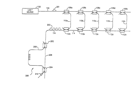
The optical source of Figure 1 is pulsed to producean input pulse 201 which is distributed to the Yarious
sensors 110 via input bus 102 and directional couplers
108a - 10~n. As the pulse 201 traYels down line 102 and
is distributed to the various sensors 110, a string Or
pulses 203 is produced on return bus 114 with each pulse
in the string coming from a difrerent sensor 110. The
spacing between each pulse in the string 203 is based upon
the optical path difference bet~een adjacent sensors
25 110. Thus, the first pulse in the string will correspond
to the pulse which was communicated through sensor 110a,
since this optical pulse had the shortest travel time
between the light source 100 and ~he return bus 114.
~ ike~lse, the second optical pulse corresponds to the
pulse pro~ided from sensor 110b, since this pulse had the
next shortest optlcal path iength from the ~i6ht source
100 to return bus 114. ~he sp3cing Or the pulses in thls
embodiment is not based on the coherence length Or the
optical source since this pulsed system is not coherence
dependent. Thererore, an optical source Or any Or a broad
range Or coherence len6ths may be used in this embodiment.
lZ~91!~
or course, the pulse length Or the pulses rrom the
light source 100 should be adjusted so that the return
pulses rrom the sensors do not overlap with each other.
Further> the pulses rrom light source 100 should be timed
so that the return pulses from the sensors do not overlap
with pulses rrom the next sampling of the array. ~or
example, if the pulse length from light source 100 ~ere
too long, the length of the pulse communicated from sensor
110a onto return bus 114 may be such that the tail of the
pulse would not be placed on bus 114 at coupler 112a
before the leading edge of the pulse from sensor 110b
passes through coupler 112a on return bus 114. Likewise,
if the timinB Or the pulses from light source 100 is too
close together, the output pulse rrom sensor 110a
corresponding to the second pulse rrom the li3ht source
could be placed on the return bus 114 before the output
pulse rrom sensor 110n corresponding to the first pulse
rrom light source 100 passes couplers 112a on the return
bus 114. In either Or these situations, it would be
virtually impossible ror a detector, receiving the pulses
from the return bus 114, to determine which sensor those
pulses had been received from.
The string of pulses 203 is transmitted along riber-
optic return bus 114 to the input Or a ~.ach-Zehnder
interferometer 200 ~hich is comprised of a pair Or
directional couplers 202 and 204 positioned on the riber-
optic return bus 11~ so as to define a first arm 206
between the couplers. A second len~th o~ optical fiber
208 is secured at either of its ends in the couplers 202
and 204 so as to define a second arm Or the interrerometer
betheen couplers 202 and 204. The dirference in optical
path lengths Or arms 206 and 208 should substantially
equal the difference bet~een optical path len~ths Or
successi~e sensors. 0ptionally, arm 206 coud be Or a
lenth greater than arm 208 by an amount ~hich
-17-
~z~ 9
substantially equals the dirference between the optical
path lengths Or successive sensors.
With the arm lengths chosen as described above, the
pulses pass through interferometer 200 such that the
portion of the rirst pulse rrom string 203 which traverses
the longer arm 208 reaches coupler 204 at substantially
the same time as does the portion Or the second pulse from
string 203 which traverses the shorter arm 206. Likewise,
the portion Or that second pulse which traverses arm 210
arrives at the coupler 204 substantially at the same time
as does the portion Or the third signal from string 203
whi ch traverses arm 206. Thus, it is seen that the
interferometer 200 ~ill cause mixing in the optical
coupler 204 of the output signals from adjacent sensors.
The mixed signal which is output rrom coupler 204 is
communicated to a detector 212 positioned on that portion
of fiber 208 ~hich extends beyond coupler 204.
Optionally, detector 212 could be posltioned on the
portion Or fiber 114 which continues beyond coupler 204
rrom riber 206. Still rurther, t~in detectors 212 could
be positioned one each on the detector locations just
descri bed.
The detector 212 receives the mixed signal, ~hich
represents the gradi ent Or the environmental paraDleter
influencing the related sensor. One preferred embodiment
Or a detector for use in the system of the present
invention may comprise a model MFOD2401~ detector
preamplirier, commercially available rrom l~;otorola
Semiconductors, Phoenix, Arizona. or course, connected to
30 the output Or the detector 212 for each Or the embodiments
Or the invention is appropriate measuring equip~ent (not
sho~n) Or a type ~hi ch is generally used in the techno!o6y
ror monitoring and e~aluating such optical output signals.
In the e~bodiments illustrated here~n, the optic21
35 path length dirferences bet~een adjacent optical paths are
--18--
~Z~ lg
made to conform with the optical path length difrerence ln
interferometer 200. By so doing, and with proper spacing
of the paths andior proper timing Or p~lses rrom the
optical source, all pulses returning from the sensing
regions can be processed through a single interferometer
200. Howe~er, ir the difrerence between adjacent optical
path lengths in the sensing region is not substantially
the same as the path length difference Or interrerOmeter
200, then other interrerometers can be optically coupled
to return bus 114 to define path length dirferences ~hich
correspond ~ith those other path length difrerences in the
sensor region. Such additional interferometers could be
optically coupled either in parallel or series
configuration with interferometer 200 on ~a~eSuide 114.
System performance is Breatly enhanced; and
undesirable conditions such as phase induced intensity
noise are minimized by tbe ability to closely match the
optical path length difrerence in compensating
interferometer 200 ~ith the optical path length difrerence
between optical signals to be combined in the
interrerometer 20~. Yarious techniques and systems are
generally known in the lndustry ror matching these optical
path length differences. One prererred embDdiment Or a
method and system for accomplishing thi~ close matching is
disclosed in Tur, et ~l., Electronics Le~ters, Vol. 22, No.
15, Jul~ 17, 1986.
In the embodiment of F~8~re 1, as ~ell as ln the
other embodiments described herein; a freq~ency shifter
(not shown) may optionaily be positioned in the s~stem,
S such as on one arm of the compensating interferometer.
~z~
The frequency shirter is utilized to shift the fre~uency
of the optical signal and, therefore, to "heterodyne" the
matched optical signal detected by detector 212. By
heterodynin~, the phase modulated output signal enters the
detector 212 as a comparatively lou frequency phase
modulation Or a hi6her rrequency arplitude modulated
optical signal. Heterodyning provides a method by uhich
lower frequency environmental effects can be prevented
from reducing the system's sensitivity to small signals in
the desired frequency range. Thus, those environmental
effects in the desired frequency range can more readily be
identified.
One preferred embodiment of a frequency shifter ~hich
may be utilized for this purpose is a Bragg Cell
modulator, which is uell-known in the technology, many
types of which are commercially available. Such frequency
shifters are comprised of bulk optics, which are inserted
into the system by separating the fiber. Light is coupled
to and from such bulk optic devices by lenses. It becomes
apparent that the use of bulk optics such as Bragg Cells
ror frequency shifters increases the system loss and
reduces overall efriciency and quality of performance.
Another technique for accomplishing heterodyning in the
coherence distributed sensor Or the present inventior"
without the necessity of frequency shifters and uithout
experiencing the losses involved with the use Or bulk
optics, is described in detail subsequently uith reference
to Figure 8.
With respect to the coupling of light signals in the
present invention, a more detailed description Or a
prererred riber-optic directional coupler which may
comprise couplers 108 and 112, for exarple, Gay be
provided by reference to Fieure 2. Specifically, this
coupler comprlses tuo optical fiber strands labeled 150a
and ~50b in Fi~ure 2 Or a sin~le mode riber-optic r~aterial
-20-
f ~
having a portion of the cladding remoYed from one side
thereof. The two strands 150a and 150b are mounted in
respective arcuate slots 152a and 152b, formed in
respective blocks 153a and 153b. The strands 150a and
150b are positioned with the portions Or the strznds uhere
the cladding has been removed in close-spaced
relationship, to form a region Or interaction 154 in which
the light is transferred between the core portions Or the
strands. The amount Or material removed is such that the
core portion Or each strand 150a and 150b is within the
evanescent field of the other. The center-to-center
spacing between the strands at the center Or the coupler
is typically less than about 2 to 3 core diameters.
It is important to note that the light transferred
between the strands at the reeion Or interaction 154 is
directional. That is, substantially all Or the light
applied to input port A is delivered to the output ports B
and D without contra-directional coupling to port C.
Likewise, substantially all Or the light applied to input
port C is delivered to the output ports B and D. Further,
- this dir~ctivity is symmetrical. Thus, light supplied to
either input port B or input port D is deli~ered to the
output ports A and C. Moreover, the coupler is
essentially nondiscriminatory uith respect to
polarizations, and thus preserves the polarization cf the
coupled light. Thus, for example, if a light bea~ haYing
a ~ertical polarization is input to port A, the light
coupled from port A tv port D, as well as the light
passing straight through from port A to port B, uill
remain ~ertically polarlzed.
From the roreEoing, it can be seen that the coupler
may function as a bezm splitter to divide the applied
light into tuo optical paths, as is accomplished by
coupler 104 Or Fi6ure 1.
-21-
lZ~
In the embodiment shown in Figure 2, the coupler has
a coupling efriciency which may be varied based on the
positioning Or the fibers with respect to each other. As
used herein, the term "coupling efficiency" is defined as
the power ratio of the coupled power to the total output
power, expressed as a percent. For example, referring to
Figure 2, if light is applied to port A, the coupling
efficiency would be equal to the ratio of the power at
port D to the sum of the power output at ports B and D.
In the distributed sensor Or the present invention,
careful adjustment Or the relative path lengths and of the
coupling efficiencies Or the couplers is required to
achieYe optimum efficiency and performance.
Another preferred embodiment Or the distributed
15sensor system is illustrated in Figure 3. In this
embodiment, a light source 100 such as a continuous wave
optical laser is optically connected to an optical ~ate
101 for producing pulsed optical signals. The optical
gate 101 is optically connected Yia a line 103 to a fiber-
- - 20optic input bus 102. Secured in spaced relationship along
input bus 102 are a plurality of optical couplers 108a,
108b, 108c, ... 108n which optically connect bus 102 to a
plurality Or sensors 110a, 110b, 110c, ... 110n which
themselves are optically coupled via a plurality Or
optical couplers 112a, 112b, 112c, .. 112n to a riber-
optic return bus i14. This configuration corresponds to
the ladder network of the sensor arm Or the embodiment
illustrated in l~igure ~.
Portions of the input bus 102 between sets Or
30 couplers 108 are configured in a coil arrangement
~enerally indicated at 105. The coils 105 comprise delay
lines for definin6 the difference in si~nal path length
tra~eled by optical signals passing in adjacent sensor
arms 110. In addition, at least a portiDn Or each Or the
35 colls 105 is not enviror,mentally shielde~, thereby forming
~Z~
a sensor located on the input bus. By positioning the
sensors and delay lines on the input bus, the number Or
optical components required in this ladder portion Or the
structure is minimized. Also, by positioning the sensors
on the input bus, every pulse on the return bus 114 except
the first and last pulse corresponding to a given pulse
rrom the light source can provide inrormation rrom an
individual sensor so that differences in phase between
adjacent pulses on return bus 114 derine environmental
conditions influencing a particuiar sensor. In contrast
to the embodiment illustrated in Figure 1, uhich provides
a measure of the difference in the environment betueen
sensors 110a and 110b, for example, the embodiment
illustrated in Figure 3 provides a direct measure Or the
environment at sensor 105.
For e~ample, when an optical pulse 203 having
traveled the optical path through arm 110b is combined
with a pulse 203 having traveled the optical path through
- arm 110a, the phase dirference signal provided rrom
coupler 204 will directly relate to the environmental
errect influencing the pulse which passed through the
sensing region 105 between couplers 108a and 108b. This
occurs because both combined pulses traveled a common
optical path through any other sensing regions in their
path on waveguide 102, however, only one sisnal in this
pair passed through the sensor between couplers 108a and
108b. Thererore, the phase change caused in that si~nal
uhlle passing through that sensor uill be directly
evidenced by the phase difrerence signal rrom coupler 204.
By providing sensor inrormation for a 61ven sensor on
all but the first and last pulses on the return bus 114,
as lndicated above, the output duty c~cle can be
sub~tantlally optimized ln the configuration Or ~igure
3. ~hls is accomplished by spacing the sensors 110 uith
respect to each cther so that the optical p3th lensth
lZ~913
difrerences between adjacent sensors are substantially the
same for each sensor pair. Thus, all but the rirst and
last signal rrom a pulse 201 can be used in the
compensating inteferometer 200 to deYelop sensor
information. This duty cycle can be further optimized by
timing the optical pulse signal rrom the light source 100
so that the resulting pulse signal placed on return bus
114 from rung 110a immediately follows the passage of the
pulse on bus 114 rrom arm 110n, and is synchronized
therewith, thereby reducing the minimum time between
transmission Or pulses rrom the otpical source.
Return bus 114 is connected to provide the optical
signals traveling therein to a Mach-Zehnder interferometer
200 which corresponds to the interrerometer described ~ith
rererence to Figure 1. As with the configuration of
Figure 1, the adjacent signals communicated to
interrerometer 200 from return bus 114 are mixed to
provide an output from coupler 204 ~hich is communicated
to a detector 212. The mixed signal comprises a phase
difference signal which represents the environmental
parameter inrluencing the sensor through which only one of
the adjacent signals has passed.
As with the configuration o~ Figure 1, the difrerence
in optlcal path lengths traveled by the optical signal
bet~een adjacent sensors should substantially equal the
path length difrerence of the arms 206 and 208 Or the
interrerometer 200.
In operation, a li~ht source 100 such as a laser
diode communicates a continuous wave optical signal to the
optical gate 101. Cate 101 gates the optical-sisnal to
produce a series Or pulsed output signals at a rate and
signal length which will avoid the sisnal overlappin6
problemQ described earlier. One such optical pulse si6nal
i~ illustrated at 201. The optical pulse 201 is
communicated via lens 103 into the input bus 102. As the
lZ~i919
optical signal 201 continues to travel down input bus 102,
portions Or it are transmitted via couplers 108 through
sensors 110 and couplers 112 to the fiber-optic return bus
114 in the manner preYiously described with respect ~o
Figure 1. The signals returning on bus 114 comprise a
signal train illustrated at 203, with the signals spaced
at intervals such that interference will occur between
adjacent signals at coupler 204, rollowing transmission Or
the signals through the interferometer 200.
Optionally, a frequency shifter (not sho~n) may be
included in the riber delay line 206 or 208 Or the
embodiment of Figure 3, thereby providing a heterodyned
signal as was previously discussed with respect to Fi~ure
1.
~ Another preferred embodiment Or the distributed
sensor system Or the present invention can be described by
reference to Figure 4. The system Or Figure 4 is
configured substantially identically to the system Or
Figure 3, except that the portions Or input bus 102
between adjacent couplers 108 comprise only delay lines
- generally indicated at 107. These portions are not
exposed to environmental inrluence, as was the case in the
device Or Figure 3. The senslng is accomplished in the
illustrated embodiment by constructing ~ach-Zehnder
interrerometers such as t~ose illustrated generally at
lOga, lO9b, 109c, ... 109n on the rungs 110 of the ladder
.
conriguration.
Y.ore specirically, each rung 110 comprises a rirst
optical coupler llla, 111b, lllC, ... 111n, and a second
optical coupler 113a, 113b, 113c, ...... 113n, ~hich derine
the length Or a rirst arm 115a, 115b, 115c, ... 115n Or
the interrerometer 109. Also connected at opposite ends
to the couplers 111 and 113 on each rung 110 is a second
arm Or the interrerometer comprising a sensin~ arm 117a,
117b, 117c, .... 117n.
-25-
~2~
Preferably, the optical path length dirrerence
between the arms in each of the sensing interrerometers
109 is substantially identical to the optical path length
difrerence between the arms of the com.pensating
interrerometer 200.
In operation, a series Or pulsed optical signals such
as the pulse signal illustrated at 201 is produced and
transmitted into the input bus 102 in the ~anner
previously described with respect to Figures 1 and 3. As
the optical signal 201 travels down the input bus 102, a
portion of the signal is coupled via couplers 108 into the
rungs 110. The signal in each Or the rungs 110 is
communicated through the interrerometer 109 Or that rung,
with the result that a portion Or the signal is
communicated through the first arm 115, with another
portion going through the second, sensing arm 117. ~he
output rrom each interrerometer is communicated via
couplers 112 onto the return bus 114. This output
comprises a pair Or optical pulse signals 205a, 205b,
205c, ..... 205n ror each signal communicated into the
sensing interrerometer 10g. Each pair of optical pulse
signals 205 travels down output bus 114 and is received in
the compensating interrerometer 200.
With the optical path length difrerence Or the
interrerometer 200 matched to each Or the path length
dirrerences Or the interrerometers 109, the pair Or
optical pulse signals 205 produce a pair Or signals uhich
are caused to constructively interrere in coupler 204, to
produce a phase difrerence signal on the output Or coupler
204. This phase difrerence output is representative Or
the phase dir~erence Or the palr Or signals 205 arter
traverslng the separate arms Or their particular
interferometer 109. Accordingly, the phase d1rrerence
signal indicates the environmental efrect on the
particular sensor arm 117 Or the interferometer 109 ~hich
-26-
~296919
influenced the phase Or the signal passing therethrough.
~he phase difference signal rrom coupler 204 is
communicated to the detector 212, from uhence it is
communicated to processing equipment for use in evaluating
the environmental parameter which influenced the sensing
arm of the interferometer 109 through which the signal
pair traveled.
Because each rung 110 contains its own ~ach-Zehnder
interrerometer, and so long as the rungs are spaced
sufriciently and signal pulses are separated properly to
prevent signal overlap on the return bus 114, the
monitoring of environmental efrects on a particular
sensing interferometer 109 is accomplished uithout sensing
involvement of signals from any other sensing
interrerometer 109. As a result, there is essentially no
restriction on the length Or the input bus 102, or the
output bus 114, between adjacent rungs of the system.
Accordingly, a distributed sensor such as that disclosed
with reference to Figure 4 rinds particular value in
applications requiring sensors to be located at selected
points which may not be equidistant rrom one another, and
uhich may be at extended distances from the light source
100 or rrom the compensating interferometer 200.
It is noted that in the system Or Figure 4, like the
arrangement or the other embodiments disclosed herein, the
optical signal is a pulsed signal. Therefore, the
pos~tioning Or the couplers 108 and rungs 110 is not
dependent upon the source coherence length Or the light
source. However, the pulses from light source 100 should
be tlmed such that the pulses returning- to the
compensating interferometer 200 do not overlap each other,
nor interfere uith pulses produced by the next pulse from
li~ht source 100.
Rererrin6 no~ to Figure ~, another embodiment Or the
device uhich is the equivalent Or the embodiment of Fi~ure
-27-
lZ9~919
3 may be described. Specirically, like the embodiment Or
Figure 3, the system illustrated in Figure 5 includes a
light source 100 which can comprise a self-pulsed laser
ror producing a pulsed optical signal, or which can
comprise a continuous wave laser optically connected to an
optical gate 101 for electronically or mechanically gatin6
the optical signal to produce a pulsed optical output.
~he pulsed optical signal is communicated via lens 103 to
an optical riber input bus 102.
A rirst optical coupler 104 is positioned on input
bus 102 and is connected to one end Or an optical fiber
comprising a return bus 207 such that optical signals are
coupled between the input bus 102 and the return bus 2~7
15through coupler 104. Return bus 207 is optically
connected at its other end to a Mach-Zehnder
interrerometer 200 which corresponds in conriguration to
the interrerometer 200 previously described with respect
to the embodiments Or Figures l, 3 and 4. The output Or
the interrerometer 200 is also connected to a detector 212
in the manner previously described.
- Also positioned at selected locations on input bus
102 are a plurality Or optical couplers 108a, 108b, 108c,
... 108n. Couplers 108 are each connected to a first end
Or an optical riber 220a, 220b9 220c, ... 220n. ~he other
end Or each Or the optical fibers 220 is optically
connected to a reflectiYe mirror 222a, 222b, 222c, ...
222n. Rerlective mirrors 222 are positioned in a
conri6uration so as to directly rerlect li~ht travelin6
dounward throu~h optical ribers 220 back in the opposite
dlrectlon throu~h ribers 220. Such mirrors may comprise
metal or other rerlectiYe m~aterial ~hich ls deposited
dlrectly on the fiber end. ~he optical ribers 220 are
approxlmately 1/2 as long as the rungs 110 Or Figure 3.
Thu~, the total optical path traversed by an optical
35~16nal enterin6 one Or the optical ribers 220 and thcn
-2~-
lZ~ I9
rerlected back through the optical fiber 220 would be
substantially the same distance as the optical path of
light traveling through the corresponding rung 110 Or the
embodiment of Figure 3.
At positions between adjacent optical couplers 108,
the input bus 102 i9 configured to form a delay line uhich
creates an optical path of a desired length. At least a
portion Or each delay line is exposed to the environment
or is otherwise configured to be susceptible to
environmental influence, so as to define a sensor for
imprinting environmental information on optical signals
traveling ~ithin the sensing portion of the input bus
102. The optical path length defined by the delay line
224 is selected to create an optical path length
difference between paths of optical signals reflected
through adjacent optical fibers 220 which corresponds to
the optical path length difrerence between the arms Or the
compensating interferometer 200.
Accordingly, since the signal reflected from mirror
222 through fiber 220 tra~els the delay and sensing
- portion twice~ the length of each delay coil 224 as uell
as the length Or each portion Or bus 102 which is exposed
to enYironmental influence should be approximately 1/2 the
length of the corresponding delay coils and sensor regions
105 of Figure 3. The number Or optical fibers 220 and
delay portions 224 are selected based upon the number of
difrerent locations to be monitored, or the number Or
en~ironmental sensors to be monitored.
The relationship between the adjacent optical fibers
220 ln this conriguration corresponds to a ~;ichelson
lnterrerometer. For exzmple, the portion Or the device Or
Figure 5 derined by optical coupler 108a, optical fiber
220a, and rerlecti~e mirror 222a, in combination ~ith
Input bus 102, delay line and sensor 224, and optical
riber 220b and associated mirror 222b define a
lZ~
conventional Michelson interferometer. Thus, optical
signals rerlected from the optical ribers 220 are
communicated back onto input bus 102 and then through
coupler 104 onto the free end 235 Or return bus 207 to
produce a series Or optical signals similar to those
produced on return bus 114 Or Figure 3.
More specifically, in operation of the device Or
Figure 5, an optical pulse 201 is communicated rrom the
light source 100 and optical gate 101 through lens 103 to
the optical input bus 102. Although a portion Or the
optical signal 201 is communicated via coupler 104 onto
return bus 207, the remainder Or the optical signal 201
travels down input bus 102 and is partially coupled in
each Or the couplers 108 onto its associated optical fiber
220. In each case, the signal on optical fiber 220 is
reflected by the reflective mirror 222 so as to return
throu~h the optical riber 220 and again be coupled through
coupler 108 onto the inpuS bus 102. These rerlected
signals travel along input bus 102 toward the optical
signal source 100 and are partially coupled through
coupler 104 onto return bus 207. As a result, a strin6 o~
optical pulses 203 are communicated rrom the system onto
the return bus 207. Since each Or the optical ribers 220
are hal~ the length Or the rungs 110 Or Fi6ure 3, and
since the delay and sensor portions 224 are half as long
a~ the corresponding delay and sensor portions 105 Or
Figure 3, the optical path of each Or the signals 203 on
return bus 207 will correspond to the path len~th traveled
by the optical pulse signals 203 Or Figure 3.
The optical pulse si6nals 203 are communicated from
return bus 207 into interrerometer 200 and p.ocessed in
the manner previously described ith respect to Fi~ure
3. The resultin~ signal detected by detector 212 rro~ the
output Or interferGmeter 200 pro~ides a phase ~i'rerence
sisnal representative oS the environmental influence on
-30-
the optical sensor located between the two adjacent
optical ribers 220 traveled by the two optical signals
combined in the coupler 204 of interferometer 200.
It will be appreciated that the embodiment Or Figure
accomplishes substantially the same runction and
operation as the ladder confi6uration Or the device Or
Figure 3, but does it without the use Or a return bus
connected to each Or a plurality of ladder-type rungs.
Howe~er, the embodiment Or Figure 5 does cause the optical
signals to each pass through one additional coupler 104,
since the input signal passes through this coupler after
being coupled onto the input bus 102, and the signals
reflected rrom the optical ribers 220 also pass through
that coupler 10~. As a result, the embodiment Or Figure S
experiences about a 6dB loss in perrormance as compared to
the embodiment Or Figure 3.
The embodiment Or the invention illustrated in Figure
4 can also be modified by replacing the return bus 114 and
sensing Mach-Zehnder interferometers with equivalent
Michelson interferometers. The embodiment ror
accomplishing this can best be described by rererence to
Figure 6. As with the previous embodiments Or the
invention, this system also utilizes a pulsed light source
100 which can comprise either a continuous wave laser
~hich is electronically or mechanically pulsed by means
such as an optical gate 101, or through use Or a self-
pulsed laser. In either conri6uration, the pulsed optical
signal is communicated from the self-pulsed optical laser
100, or the optical gate 101 through a lens 103 to an
optical input fiber 102. Positloned on the input riber is
an optical coupler ~04 ~hich is connected to one end Or an
optical riber return bus 207. ~eturn bus 207 is optically
connected to a compensating in~erferometer 200 ana then to
an optlcal detector 212 ~hich are substantially identical
to the corresponding interferometer 200 and àe~ec~or 212
of the embodiments Or the invention described pre~ioucly.
lZ~q~
Also positioned on optical input bus 102 are a
plurality Or optical couplers 108a, 108b, 108c, ...
lO~n. Each of the optical couplers is connected so as to
couple optical signals from the input bus 102 to an end Or
an optical fiber 220a, 220b, 220c, ... 220n. Positioned
on optical ribers 220 is an optical coupler 2213, 221b,
221c, ... 221n, coupling light between the optical riber
220 and the end of a sensing arm 227a, 227b, 227c, ...
227n of a Michelson interferometer. At least a portion of
the sensing arm 227 Or each Michelson interferometer is
exposed to environmental influences, so as to sense those
influences by changing the optical phase Or light
traveling within the arm 227 in response to environmental
influences. The other arm of the Michelson interferometer
comprises a continuation of the optical riber 220, and is
illustrated at 225a, 225b, 225c, ... 225n. The other end
of each Or arms 225 and 227 is terminated by a connection
to reflective mirrors 222, which are configured to reflect
light received rrom arms 225 or 227 back into those
respective arms.
A portion of the input bus 102 betueen pairs Or
couplers 108 may extend to ~hatever length is necessary in
order to position the sensors in their desired sensin~
locations.
To make the system of Figure 6 equivalent to the
embodiment illustrated in Figure 4, the length o~ sensing
interferometer arms 225 and 227 should be approximately
1/2 the length of corresponding sensing interferometer
arms 115 and 117, respectively, of Figurc q. In this
configuration, the optical signals transmitted into the
arms 225 and 227 of the sensing Michelson interrerometers
and reflected back tnrough those arms ~ill have tra~eled
substantially the equiYalent path length as in thc
correspondin6 Mach-Zehnder interrerometers 109 Or Figurc
4.
lZ~9~C3
In operation, the light source 100 and optical gate
101 communicate via lens 103 a pulsed optical signal 201
onto the optical input bus 102. A portion Or the optical
pulse signal 201 is communicated through coupler 104 on to
the free end 235 on return bus 207. The remaining portion
Or pulse 201 travels doun bus 102 and portions Or this
signal are coupled in each Or the couplers 108 onto
optical fibers 220 and into the associated ~.ichelson
interferometers defined by arms 225 and 227. The signals
rerlected from those Michelson interferometers are again
coupled via couplers 1D8 onto the input bus 102, with each
interrerometer producing a pair of optical pulse signals
205a, 205b, 205c, ... 205n for transmission onto input bus
102. The optical signals 205 are coupled in optical
15 coupler 104 onto return bus 207, rrom whence they pass
into the Mach-Zehnder interrerometer 200 and are processed
- in the manner previously described with respect to Figure
4. As with the system Or Figure ~, the optical signal
detected by detector 212 comprises a phase difrerence
~ 20 signal representative Or the environmental parameters
inrluencing the sensing arm 227 Or the Michelson
interrerometer which produced the pair of optical signals
205 c~rrently combined in the output rrom interrerometer
200.
As with the embodiment Or the device illustrated in
F~gure 4, the embodiment Or Figure 6 permits positioning
Or the sensing interrerometers at any desired location
such that spacing between adjacent couplers 108 is
sufriciently great so that optical signals 205 coupled
30 onto bus 102 by a given coupler 10~ do not o~erlap or
interrere ~ith optical si~nals coupled onto bus 208 by
other optical couplers 108O
The presence Or coupler 104 on the input bus 102
comprises one additional coupler uhich the optlcal signals
must pass through as compared to the embodi~ent Or Figure
lZ~369~.9
b. Accordingly, the system Or Figure 6 sufrers
approximately a 6dB loss in perrormance as compared to the
performance Or the embodiment of Figure 4.
In the embodiments described thus far, the
compensating interferometer 200 is optically coupled to
the return bus 114. However, the coupling interrerometer
200 could also be optically coupled to the input bus 102,
between the optical signal source 100 and the first
optical coupler on the bus 102. That configuration would
produce substantially the same results as the
configurations described above.
One example Or an embodiment Or the device which
includes the compensating interferometer 200 positioned on
the input bus 102 may be described by reference to Figure
7. The e~bodiment of Fieure 7 comprises the embodiment
illustrated in Figure 3, with the compensating
interferometer 200 repositioned such that the optical
signal communicated through lens 103 is coupled into the
input of interrerometer 200 at coupler 202. The signal
from interferometer 200 is optically coupled in coupler
204 to the optical input bus 102.
With the compensating interrerometer 200 located on
the input bus 102 in Figure 7, the return bus 114 is
directly coupled to detector 212. Except for the chanses
described above, no further modifications Or the device as
conrigured in Figure 3 are included in the embodiment Or
Figure 7.
In operation, an optical pulse 201 is communicated
from the light source 100 and optionally the optical ~ate
101 via lens 103 to the input Or coupler 202. A portion
of optical signal 20~ is coupled into ar~ 208 Or
interrerometer 200, uhile the remainder Or pulse 201
travels through arm 20~ o~ the interferometer. ~he pulses
from arms 208 and 206 are coupled on to input bus 102 in
coupler 204. The result Or this couplins p^ocess is a
~296919
pair Or pulsed optical signals 241 which traYel down input
bus 102 in the same manner as signal 201 doeR in the
embodiment illustrated in Figure 3. Specifically, a
portion Or each Or the pair Or pulsed optical signals 241
is coupled in each Or the optical couplers 108 into each
Or the arms 110. Since the optical path length traveled
by signals ~hich propagate through adjacent arm~ 110
corresponds to the optical path length dirrerence Or
interrerometer 2QO, the pair of signals 241 returning on
bus 114 from propagation through adjacent arms such as
11Oa and 11Ob are combined in their associated common
coupler, such as coupler 112a. As a result of this
coupling, those portions Or the pulsed signals 241 which
have traveled the same optical path lengths are coherently
coupled to form an output signal 243.
Signal 243 comprises a phase difrerence signal
representing the environmental efrects which influenced
the phase Or the portion of signal 241 propagating through
~ the sensor region 105 Or the optical path derined through
arm 110. As is the case in the embodiment Or Figure 3,
only one Or the signals ~hich are coherently coupled to
form the phase di~rerence signal 243 have traveled through
the sensing region 105. Accordingly, the phase dirrerence
value Or signal 243 $s representati~e Or those
environmental effects influencing the sensor region 105.
The phase difrerence signal 243 is communicated ~ia
return bus 114 to detector 212 and processed in the sa~e
manner as the phase dirference signal generated by coupler
204 in Figure 3.
The results produced by the embodiment Or Fi&ure 7,
~ith compensating interrerometer 200 positioned on the
lnput bus 102 are substantially identical to the results
obtained rrom the embodiment Or the system illustrated in
~igure 3, with the sensing interrerometer 200 positioned
on the output bus 114. Like~ise, subst2ntially identical
~Z96~g
results are obtained from the other embodiments Or the
invention, when the compensating interrerometer 200 is
positioned on the input bus 102, rather than on the output
bus 114.
In each Or the confi&urations Or the present
invention, the compensating interferometer 200 is
preferably shielded from environmental conditions which
may influence the phase of light waves being transmitted
therethrough. In addition, such environmental shielding
can be used on the non-sensing arms 115 and 225 Or the
embodiments of Figure~ 4 and 6, respectively, as well as
on the non-sensing portions of sensing arms Or all Or the
embodiments particularly when these arms are very long.
Use Or shielding as described above will increase the
sensitivity of the system, although such shielding is not
required for system operability. ~o other shielding for
this purpose is required in these systems, since the
systems are environmentally insensitive except in those
~ portions Or a system where signals to be combined in the
2~ compensating interferometer are traveling in dirferent
paths. This insensitivity is due to the fact that in
optical signals in the system which are communicated along
a common path, environmental influences arrecting the
light signals in the common path ~ill not produce any
changes in the phase difrerence between the light signals
in those paths. Changes in phase difrerence will only
occur uhen the light is traveling in dirferent paths, and
then only ln the sensors and portions Or those difrerent
paths which are arrected by influences such as
en~lronmental effects.
Each Or the configurations Or the lnvention described
herein co~prise a representatlve embodiQent Or the
inventlon. It will be appreciated that these
conri6uratlons can be expanded as necessary by adding
rurthcr couplers and associated sensin6 sections in the
repet~tive confi6urations ~llustrated.
-36-
~.z9G~
Based on the above description, it becomes apparent
that each of the embodiment~ Or the invention disclosed
herein derines a distributed sensor system which is lead
insensitive, and therefore requires only a minimum amount
of enYiron~ental shielding. These conrigurations also
describe an all fiber-optic sensor system which is rree
rrom both source phase-induced intensity noise and
crosstalk between sensors.
It will be noted that each sensor has a rree end rrom
which light may escape. Although this introduces loss, it
is not a serious problem since, even ror a large number Or
sensors, power loss can be kept relatively modest by
properly selecting the coupling constants Or the
directional couplers. The method ror selecting these
1~ coupling constants is explained in detail hereinarter.
Selecting Coupling Coefricients
An issue relevant to the design Or a coherence
multiplexed distributed sensor system, is the proper
selection Or coupling coerficients ror the various
directional couplers used in the system. As used herein,
- the term "coupling coefricient" is defined as the power
ratio Or the coupled power to the total output power. For
example, rererring to Figure 2, ir light is applied to
port A, the coupling coerficient would be equal to the
ratio Or the power at port D to the sum Or the output at
ports B and D.
The determination Or the coupling coerricients may be
based ~n part on the intuiti~e requirement that all
sensors experiencing equal environmental modulation
amplitudes should return signals Or comparable strength to
the central processing location.
Using the embodIment Or Figure 1 as an example,
assume that there are N sensors 110. Number the sensors
uith an index j running rrom 1 to N, startin~ ~ith j - 1
3S for the sensor closest to the light source 100 and to the
lZ96~9
compensating interferometer 200. Let the power coupling
coerricient for the couplers 108 and 112 associated wi~h
sensor j be kj, so that a fractional portion kj Or the
total power is transrerred between the two fibers in the
coupler, and an amount Or power 1-kj passes straight
through the coupler, without being coupled. It is noted
the couplers at the ends Or a given optical riber sensor
should be identical.
It is assumed for simplicity that light must couple
across fibers in the couplers 108 in order to get from the
input bus 1~2 to a sensing fiber 11~ and back to the
return bus 114, although the situation could just as well
be reversed. Light returning from sensor j will have
sufrered loss rrom couplers 1 through j on both the input
bus 102 and the return bus 114. Couplers 1 through j-1
will have a transmission 1~kq ror both the input and
return couplers 108 and 112, respectively, and the two
couplers at sensor j will have a transmission kj. Hence,
the power returning from sensor j to the receivers 120 is
given by
2 j-1
j,return Pinkj D (l~kq)2 (2)
where Pin is the power being sent to the sensor array.
g ~1,return Pj,return it is round that the
coupling coefricients are related by kjt1 ~ kj/(l-k;), or
equlvalently,
k = ~ 1 (3)
The last sensor does not really require 2ny couplers
slnce no pouer is needed ror the later sensors; hence one
can set kn ~ 1. To~ether wlth the recurslor, relation just
-38-
iZ~6~
derived, this implies that the coupling coefficlent ror
the couplers Or sensor ~ is just
k G 1 (4)
; N~
This, in turn, means that the total transmission
P~ retUrn~Pin is the same for every sensor, as expected,
and is equal to 1/N2. The ractors Or 1/N appears because
the input power has to be split up among N sensors.
The Pseudo-Heterodyne Technique For Preventin~ Si6nal
Fading
Signal rading is a signiricant problem ror all Mach-
Zehnder type sensors. One solution to this problem is to
heterodyne the signal by introducing a rrequency shirterinto one arm Or the receiver, in the manrer described
preYiously with respect to the embodiment Or Fi~ure l.
While conventional heterodyning provides one method
- 20 ror avoiding signal rading and ~or distinguishing between
si~nals in the desired rrequency range and lower frequency
environmental efrects, this approach has the disadvantage
that it requlres the use Or frequency shifters, hich
orten comprise bulk optics de~ices. Such de~ices can be
bulky, increase system loss, degrade erriciency, and can
be costly.
An easier and less expensi~e method to avoid si6nal
rading is a pseudo-heterodyne technique uhich requires no
bulk optic devices in the optical path Or the sensor
system. ~he techniq~e is derined in connection uith its
application in a riber-opt1c ~yroscope in B. Y. Kim and H.
J. Shau, "Phase-Readlng All-Fiber-Optic Gyroscope,"
Optical Letters, Vol. 9, Pa6e 378, (1984). ~he technicue
ls also disclosed in connection ~ith its application in a
39
,. .
~29~919
fiber-optic gyroscope in corresponding Canadian
Application Serial No. 479,798 filed Aprll ~3, 1985.
The application Or the technique to the distributed
sensor of the present invention can be described by
reference to Figure 8. The sensing system optically
coupled to the modulating system Or Figure 8 can
tO correspond to any Or the systems illustrated in Figures 1,
3, 4, 5 and 6. This technique also holds for the
conriguration of Figure 7, wherein the optical signals are
recei~ed by detector 212 directly from return bus 114.
Thus, only the compensating interrerometer uhich is
optically connected to those sensing system is
specirically illustrated in Fi~ure 8.
In particular, a 1 to N switch 300 is optically
connected on its input side to the output Or detector
2t2. Switch 300 runctions essentially as a multiplexer in
response to incoming signals, such that uhen a neu signal
is received rrom detector 212, the suitch 300 increments
to the next channel location uhich corresponds uith the
particular sensor ~hose en~ironmental inrormation is
represented by the signal rrom detector 212. Thus, lr the
signal inrormation rrom detector 212 ls representati~e or
the sensor inrormation communicated through a particular
arm, such as 110b Or ~igure 3, then the suitch 30D uill
output this inrormation on channel 2. Likeuise, as the
next lnrormation is recei~ed rrom detector 212, relating
to the si~nal communicated rrom arm l10C, the suitch 300
uill mo~e to the next channel and transmit the information
through corresponding channel 3. One prererred emb~diment
Or a 1 to N suitch uhich ~ay be utilized in conjunction
uith the present in-ention is a CMOS 40668 ~ET suitch
manuractured by ~ational Semiconductor.
-40-
iZ96919
Each Or the output channels from switch 300 is
connected to an identical equipment configuration.
Accordingly, the 1 to N switch is optically connected via
each Or its channels to a low pass AC amplirier 302a, ...
302n, which itself is connected to a gate circuit 304a,
... 304n for producing a square wave signal on a periodic
basis. The output Or gate 304 is electronically connected
to a spectrum analyzer 306a, ... 306n, rOr use in
identifying side bands around a harmonic of a modulation
frequency in order to monitor the phase shift in the
sensor 105 at a particular rreQuency. Alternatively, an
FM demodulator may be used instead Or the spectrum
analyzer.
The gates 304 are also connected to a signal
generator 308 uhich produces a sinusoidal signal at a
modulation rrequency fm. This signal controls periodic
production Or the square wave in the gate circuit 304.
The signal generator 308 is also connected to a phase
_ modulator 310 which is positioned in optical communication
20 with the arm 208 Or compensating interferometer 200. The
- phase modulator 310 is controlled by the signal generator
308 uhich causes the phase modulator to produce a phase
modùlation signal at the modulation rrequency rm.
Since the equipment connected to each output channel
rrom suitch 300 runctions ln an identical manner, the
operation of the equipment on a single channel uill be
described ror example purpose~. It is noted that the
optical sisnals in the system Or Figure 8, propagate and
interrere ln the manner previously described uith respect
30 to the embodiment Or Figure~ 1, 3, 4, 5 and 6 except as is
otheruise indicated belou. The description herein al~o
applies to the embodiment Or Figure 7, uherein the phase
modulator 310 is positioned on arm 208 Or the
interrerometer 200 or input bus 102. Specirically, the
light ln arm 208 is phase modulated by the phase modu1ator
-41-
1296919
310, which is driven at a modulation rrequency
corresponding to the operating rrequency of generator
308. As a result, the intensity Or the output signal rrom
coupler 204 which is received by detector 212 is
modulated, and the resulting electrical output signal from
detector 212 contains components at the phase modulation
frequency fm and its harmonics, as indicated by the
following equation:
I(t) = C[1 ~ cos(~msin ~mt + ~asin ~at ~ ~e)]
CD
[- ~ (~m) 2 ~1J2n(~m)cS 2n~mt~ cos(~a5in ~at ~
~D
- ~? ~ J2n~ m)sin (2n-1) ~mt~sin (~asin ~at ~ ~e)~
uhere C is a constant;
Jn denotes the nth order Bessel function;
~mis the amplitude Or the phase modulation betueen
- the light ~aves in arms 206 and 208 due to the phase modulator 310;
~m= 2nfm ;
~a is the amplitude of the phase dirference between
the light waves in arms 206 and 208 produced by external
acoustic signals;
~a 2nfa ; and
~els the amplitude of the phase difre.ence between
the light waves in the arms 428 and 554 produced by slou
changes in the environment.
Equation 5 indicates that the output from detector
212 contalns te.ms .ncluding: cos(~asin ~at ~ ~e) and
sln(~aSln ~at ~e) Ho~e~er, these ccsine and sine
elements are at difrerent rrequencies. Ir t~ese si6nals
were at the ~z~e frequency, ~ith their phases in
-42-
i29~ 9
quadrature, well-kno~n trigonometrlc rules could be
applied so that the signals could be added directly to
obtain a single, low rrequency, sinusoidal signal whose
phase corresponds to (~asin ~at ~e). Such a
relationship can be achieved in the system Or Figure 8
through use Or amplitude modulation. Amplitude modulation
simply involves making the amplitude Or the electrical
output signal from detector 212 vary in accordance uith
the amplitude Or a modulating signal.
When the output signal rrom detector 212 is amplitude
modulated by a modulating signal having a rrequency uhich
is an odd multiple Or the phase modulation rrequency (fm)
(uhich is also the difrerence rrequency between adjacent
harmonics), then each component Or the output signal rrom
detector 212 which is a harmonic f fm becomes partially
translated into the rrequencies Or its harmonic
neighbors. In other ~ords, through amplitude modulation
in this manner, sideband frequencies are created at
harmonics Or the phase modulation rrequency. The sideband
rrequencies are combined ~lth the component Or the output
signal at the corresponding rrequency, and are readily
identified by use Or a spectrum analyzer.
~hese and other characteristics Or amplitude
modulation are generally known to those skilled in the art
and are described ln detall in F. G. Stremler,
Introduction to_ Communication Systems, Addison-~'esley,
(1979). Subject matter of particular relevance at this
point is set forth on pages 191-260 of the Stremler
text.
Based on the abo~e, lt ~lll be appreciated that a
~lnusoidal amplitude modulation at a rrequency rm uill
transrer energy out Or each harmonic frequency component
and into the nearest harmonlc rrequPncy nei~hbors. ~o
preYent lnterrerence in the present ~ensor s~stem, lt is
desirable that rm be ~.uc~ treater than fa (the frequenc
Or acoustlc signals ~hich are being detected).
. ~
~ 43
lZ9~
In operation, the optical signal in arm 208 Or
compensating interreromeSer 200 is phase modulated at a
~requency which is controlled by rrequency generztor
308. As indicated above, the rrequency Or generator 308
is selected ~o that rm (the modulation frequency) is much
greater than the acoustical rrequency (fa) The signal
rrom arm 208 passes through coupler 204 where it is mixed
uith the signal rrom arm 206, producing an intensity
modulated signal due to the phase difference which is
passed to detector 212. From detector 212, the intensity
modulated signal due to the phase difrerence is
communicated through the 1 to N switch to amplifier 3û2
where the signal is amplified and then transmitted to the
conventional electronic gate 304.
Gate 304 functions in response to a signal recei~ed
rrom the rrequency generator 308, causing Bate 304 to
produce a square wave amplitude modulation or the signal
received rrom amplirier 302. When modulated at the
appropriate phase with respect to the AC detector current,
20 and with th~ appropriate choice Or a~m, the amplitude
modulated signal Or this embodiment may be derined as
cos(n~mt ~ (~aSin ~at ~ ~e))
~ ith respect to the appropriate phase and amplitude
for modulation, lt is noted that due to the trigonometric
5 relationships betueen the waverorms in coupler 204,
amplitude modulation at e~en harmonics Or Sm would not
produce coupling bet~een adJacent harmonic frequencies.
Rather, amplitude modulation at even harmonics Or Sm uould
result in the e~en harmonics coupllng -with even harmonics,
30 and odd harmonics coupling uith odd harmonics. This
sltuation is generally understood by those skilled in the
art, and the basls ror this condition may be :;;ore rully
understood with reference to the Stremler text. These
problems are avoided if amplitude modulation at the odd
35 harmonics is utilized.
--44--
lZ969~9
~ he output from gate 304 is communicated to the
spectrum analyzer 306 for processing. It is noted that
spectrum analyzers 306 incorporate a band pass filter for
selecting and analyzing particular components Or
signals. If such a band pass filter, centered on 2~m,
were placed on the output Or the gate, and if the
amplitude Or the phase modulation ~ were chosen
appropriately, the filter would pass a signal Or the form:
V(t)= k x ~Jo(~a)COS(2~mt-~e)
O~
+ ~ J2n(~a)[cos (2(~1~m-nwa)t-A~e)~cos (2(~m~n~"a)t-a~e) ~
.s + ~ J2n ~ a)[cos((2~1~m-(2n-~ a)t-~e)-cos((2~m~(2n~ a)t-~e)]}
(6)
~ where k is a constant which does not influence the
identirication and evaluation Or phase shirts occurring in
the sensor at particular rrequencies.
By putting the demodulated signal from the gate 304
into the spectrum analyzer 306, the height cr the Bessel
runctlon sidebands around the second harmonic Or the
modulation rrequency can be measured by use Or techniques
uhich are uell-~no~n in the technology to give the phase
~hirt in the sensor at a particular rrequency.
Alternatively, rOr a complicated signal, an FM demodulator
could be used. In that case, the measured signal uould be
the derivative Or the phase rather than the actual phase,
or alternatively, an integrator could be used to produce a
measured signal representative Or the actual phase.
Optionally, gatinB Or the system Or Figure 8 could be
accompllshed ~ptically rather than electrically by
~5 util~lng at least one optical Eate, such as a shutter,
-45-
~29~919
positioned bet~een coupler 204 and detector 212, or on any
riber in the system comprising an optical path ~here all
light signals tra~el, such as input bus 102 between the
li~ht source 1~0 and optical coupler 108a, Or Figure~ 1,
3, 4, 5 or 6, or optical fiber return bus 114 bet~een
couplers 112a and 202 Or the embodiments Or those
figures. Ir the Bate 304 were positioned distant rrom the
detector 212, the Bate should be controlled by a delay
signal at a rrequency rm so that the light traveling
within the system uould be amplitude modulated at the rm
rrequency, in appropriate phase with the distant ate. In
all other respects, the use of optical gating uould
pro~ide a result substantially identical to that described
in connection with electrical 6ating.
A simplified version or the embodiment Or Figure 3,
including the synthetic heterodyning conriguration Or
Figure 8 was constructed and tested to evaluate its
perrormance. The or~anization Or this simplirled Yersion
may be described along with the results Or the e~aluation,
by rererence to Figure 9. In the embodiment Or Figure 9,
the light source 100 comprised an essentially 3ingle-mode
laser diode comprising a ~Hitachi HLP 1400 emltting a
continuous wave 820 nm light. This light ~as communicated
through a lens 4D0 and a conventional optical isolator 402
to an acousto-optic Bra8g cell 404 corresponding to
optical 8ate 101 of Figure 3, uith a 35 nsec rise time.
The Bragg sell 404 uas used, instead Or direct modulation
Or the input current to the laser, in order to a~oid
modulation Or the laser spectrum.
The 100 nsec uide pulses uere communicated through a
lens 406 to the end Or an optical input bus 408,
corresponding to bus 102 Or Fi~ure 3.
The optical pulses uere transmitted throu6h a first
rlber-optic Yach-Zehnder interrerometer 410 ~a~lns a first
arm 412 corres~onding to arm 110a Or Figure 3. Likeuise,
Trademark
46
_
12969~9
the arm 414 Or interferometer 410 corresponds to the
optical path length derined between coupler 108a and 112a,
for the signal passing through arm 11Ob Or the embodiment
Or Figure 3. Interrerometer 410 additionally included a
phase modulator 434 in optical contact with the arm 414 Or
that interferometer. Phase modulator 434 was provided to
simulate an acoustic signal. A signal generator ror
producing the phase modulation in modulator 434 is
illustrated at 442. ~he phase modulator 434, as well as
all other phase modulators in the system correspond to the
type described previously herein.
Interferometer 410 also included polarization
controllers generally indicated at 446. These manually
adjustable polarization controllers were used to overcome
polarization induced signal-rading ror the associated
sensor. The polarization controllers correspond to those
which will be described hereafter. Optionally,
polarization preserving or polarizing fiber can be used to
_form the optical riber waveguides in the system, removing
the need ror polarization controllers 446.
Optical couplers 430 and 432 were positioned on the
input bus 408 to couple optical signals between that input
bus and the arms Or the interferometer 410. Couplers 430
and 432, as uell as all other couplers in the system,
comprised tunable directional couplers Or the type
described previously herein.
From the output Or interferometer 410 the optical
signals were communicated to another interferomeSer 420
which corresponds to the interferometer 200 of Fi~ure ô.
30Particularly, 2rm 422 Or Figure 9 corresponds to arm 206
Or the interrerometer 200 Or Figure 8. ~ikewise, arm 424
Or interrerometer 420 Or Figure 9 coFresponds to arm 20S
of the interferometer 200 Or Figure 8. ~he optical
interferometer ~20 compri~ed optical coupler~ 436 and 43
~or couplin6 optlcal sisr.als received rrom interreromete-
-47-
1296919
410 between arms 422 and 424 of the interrerometer 420.
In addition, a phase modulator 440 was positioned in
optical contact to the arm 424 of the interrerometer
420. The phase modulator 440 was used to generate
relatively high frequency modulation at the rate Or
approximately 30 kHz for the synthetic-heterodyne
demodulation technique employed avoid signal-fading caused
by phase drift.
The optical path dirference between the arms in
interrerometer 410 corresponds to the optical path
difrerence between the arms of the interrerometer 420. In
the experimental case, this relative optical path length
time delay betueen the arms in each interrerometer was
approximately 230 ns.
15Matching of the path imbalances of the two
interrerometers is important. To insure that phase-
induced intensity noise does not arise to a measurable
level on the signal pulse, it is necessary to match the
_ optical path length dirrerence Or the sensing
interferometer 410 and Or the compensating interferometer
420 to each other so that the amount Or mismatch is less
than a small rractiOn Or the coherence length Or the light
source 100. The accuracy with which riber lengths can be
matched constitutes a practical limit to the coherence
2 length Or the optical source which may be used in these
distributed sensor arrays. Measurement Or the path
difrerences in the e~aluation system Or ~igure 9 uas
accomplished by amplitude modulating a laser diode and
determining the characteristic rrequency Or the rlltering
Or each Y.ach-2ehnder individually.
In order to equalize the path difrerences, a
technique for taking small lengths Or riber rrom one arm
Or an interrerometer uas required. This ~as acco~plished
by using capill~r~ tubes to hold the fibers ror splicing,
and ~hen ~rinding do~n and resplicing the ca~illary tubes
-4S-
1%~919
containing the ribers ~hen adjustment of the length ~as
required. The capillary tu~es uere polished at an angle
to minimize rerlertion back into the laser, ~hich would
arfect the laser spectrum. The isolator 402 ~as placed
between the laser and the Bragg cell to rurther decrease
rerlections. All optical ribers in the system comprise
~Corning single-mode sensor (high N.A.) riber. The signal
~enerator for producing the modulation in phase modulator
440 is illustrated at 444. Interrerometer 420 also
included manually adjustabie polarization controllers
generally indicated at 44B, for o~ercoming polarization
induced signal fading rOr the associated sensor.
The output rrom irterferometer 420 was communicated
via a lens 450 to a Bragg cell 452 which ~as provided to
optically sample signal pulses rrom the series Or output
pulses received rrom interrerometer 420. This Bragg cell
4~2 was connected ~ia a delay line 454 to a pulse
generator 456. Pulse generator 456 ~as also connected to
- 8ragg cell 404. ~hus, the pulse generator 456 runctioned
to cause operation Or both ~ragg cell 404 and 452. She
BraBg cell 452 was pulsed synchronously with BraBg cell
404 in order to extract only the signal pulse.
The signal current receiYed through lens 4~0 in Bragg
cell 452 was communlcated to a detector 458 corresponding
to detector 212 Or ~igure 8. The signal current rrom
detector 458 was transmitted through a narro~ band uidth
(about 300 kHz) AC amplirler 460 corresponding to
amplirier 302 Or Figure 8, and into an electronic 6ate 462
corresponding to gate 304 Or Figure 8. The gate 462 ~as
connected ~ia delay line 464 to the signal generator 444,
to synchronize the ~ate 462 to the phase modulation si~nal
rrom generator 444. ~he output Or the gate 462 ~as
proYlded to a spec~rum analyzer 466 corresponding to
spectrum analyzer 306 o~ F1~ure 8.
* Trademark
-49-
129~9~9
With the amplitude of the phase modulation ror the
synthetic heterodyne demodulation adjusted to be about 2.8
radians, the phase Or the second harmonic signal received
in the spectrum analyzer 466 rrom gate 462 reflected the
optical phase difrerence between the interrering optlcal
waves. The magnitude of this signal is independent Or the
optical phase difrerence, leading to a constant
sensitivity.
The minimum detectable phase shift in the sensor was
ascertained by measuring the signal-to-noise ratio
displayed on the spectrum analyzer for a small known phase
modulation amplitude from the sensor. To calibrate the
phase modulation amplitude induced by phase modulator 434
on the optical signal, the voltage corresponding to 3.83
radians was measured at each signal frequency. Voltage at
this level nulled the rirst Bessel functi~n side band.
~he sensor sensitivity was measured with the repetition
rate Or the optical input pulses set at 1.46 MHz,
corresponding to 3 times the optical path length
difrerence in the interrerometers 410 and 420. In this
condition, no pulse was generated which contained phase-
induced intensity noise. With the repetition rate Or the
optical input pulses set at 2.18 ~Hz, corresponding to 2
times the optical path length difrerence Or the
interferometers 410 and 420, the non-signal bearing
pulses, emitted at dirferent times from the source,
overlapped and generated phase-induced intensity noise in
the pulses which were discarded.
In both sets Or measurements, the sensitiYity Or the
s~stem was below ~0 ~rad/~Hz o~er a broad range Or
rrequencies. The results Or the rirst set Or measurements
are plotted as O's in Figure 9. Like~ise, results Or the
second set Or measurements are plotted using the s~mbol X
in Figure 9.
-50-
12g691~ '
The fact that there was no signiricant dirference in
the sensitivity of the system in the tuo cases
demonstrates that the signal pulse is well separated rrom
the pulse which contains phase-induced intensity noise.
The sensitivity was round to be limited by the electronic
noise in the signal processing electronics 460 and 462.
In another set Or measure~ents, an electronic switch
was substituted for the second Bragg cell 452.
Sensitivity was again measured in this conriguration, with
1 the results indicated as ~'s in Figure 9. These results
indicate that there was no significant difference in the
sensitivity resulting from the two types Or gating.
The Polarization Controllers 446, 448
One type of polarization controller suitable for use
in the sensor system Or the present invention, such as the
embodiment of Figure 8, is illustrated in Figure 10. The
controller includes a base 570 on which a plurality of
upright blocks 572a through 572d are mounted. Between
adjacent ones Or the blocks 572, spools 574a through 574c
~ 20 are tangentially mounted on sharts 576a through 576c,
respectively. The sharts 576 are axially aligned ~ith
each other and are rotatably mounted bet~een the blocks
572. The spDols 574 are generally cylindrical and are
p~sitioned tangentially to the sharts 576.
A segment Or optical fiber 510 extends through axial
bores in the sharts 576 and is wrapped about each Or the
spools 574 to rorm three coils 578a through 578c. The
radii Or the coils 578 are `such that the fiber 510 is
stressed to rorm a birerringent medium in each Or the
coils 578. The three coils 578a through 578c may be
rotated independently Or each other about the axis Or the
sharts 574a through 574c, respectively, to adjust the
birerringence Or the fiber 510 and, thus to control the
polarlzatlon of the light passin3 through the riber 510.
The diameter and number Or turns in the coils 578 are
such that the outer coils 578a and 57~c provide a spatial
delay of one-quarter wavelength, while the ~entral coil
578d provides a spatial delay Or one-halr wavelength. The
quarter wavelength coils 578a and 578c control the
elipticity Or the polarization, and the half wavelength
coil 578d controls the direction Or polarization. This
provides a rull range of adjustment of the polarization Or
the light propagating through the fiber 510.
It will be understood, however, that the polarization
controller may be modified to provide only the two quarter
wave coils 578a and 57~c, since the direction of
polarization (otherwise provided by the central coil 578b)
may be controlled indirectly through proper adjustment of
the elipticity of polarization by means Or the t~o quarter
wave coils 578a and 57~c. Accordingly, the polarization
controllers 551 and 557 are shown in Figure 10 as
including only the two quarter wave coils 578a and 578c.
Since this configuration reduces the overall size of the
~ - 20 controllers 551 and 557, it may be advantageous ror
certain applications Or the present invention involving
space limitations.
Thus, the polarization controllers ~51 and 557
provide means for establishing, maintaining and
controlling the polari2ation Or the light within arms Or
the interferometers, such a~ arms 117 o~ interferometers
109 Or Figure 4, and arm 208 Or the compensating
inteferometer 2D0.
Summary
In summary, not only does the invention described
herein comprise a slgniricant improvement over the prior
art in monltoring environmental conditions at a plurality
of locations by use Or an optical source ~hich optionally
has a short coherence len6th, but it also oYe-comes o~her
long-existent problems in the Industry by (1) providing a
lZ9f~
system Or all-passive remote sensors permitting high duty
cycle time-domain addressing while not requiring highly
coherent light sources; (2) providing distributed sensor
array systems ~hich are free from signal fading, source
phase-induced intensity noise, crosstalk between sensors,
and downlead senstitivity; (3) providing such systems
which permit accurate sensing at remote locations without
environmental shielding Or the leads; ~4) providing for
heterodyning Or optical signals in a straightforward,
economic, and optionally all-riber-optic manner uhich
produces accurate and easily analyzed inrormation signals
for identifying environmental influences afrecting the
sensors; and ~5) providing the option Or all-riber-optic
sensor array systems, which do not require the use Or bulk
optics or Or electronic equipment at the sensor sites.
The invention may be embodied in other speciric forms
uithout departing rrOm its spirit or essential
characteristic~. The described embodiments are to be
considered in all respects only as illustrative and not
restrictive. The scope Or the invention is, thererore,
indicated by the appended claims rather than by the
foregoing description. All changes ~hich come within the
meaninB and range of equivalency Or the claims are to be
embraced withln their scope.