Note: Descriptions are shown in the official language in which they were submitted.
12~756~
NE-116-MK
( O99A/2) - 1 -
TITLE OF THE INVENTION
"Multiplexer/Demultiplexer Circuitry for LSI
Implementation"
BACKGROUND OF THE INVENTION
The present invention relates to a
multiplexer/demultiplexer for high speed switching
applications.
The multiplier stage of conventional
multiplexer/demultiplexer circuitry usually comprises a
sync pattern generator, an address counter and an array
of gates. The address counter is reset at frame
intervals by a sync from the frame pattern generator to
successively increment its count at slot intervals to
generate a binary count. The output of the counter is
used as an address for accessing each of the multiplexer
gates for multiplexing data bits into specified time
slots of a data bit stream. The demultiplexer stage of
the circuitry includes an array of gates, a frame
synchronizer and a second counter. The frame
synchronizer detects the sync pattern of the data bit
stream to cause the second counter to synchronize with
the slot timing of the bit stream to increment its binary
count. The demultiplexer gates are respectively enabled
by the address counts of the second counter to
demultiplex the individual data bits into output
terminals.
LSI chips currently available for high speed
switching operations have a level of integration which is
lower than is required for implementing multiplexers and
demultiplexers of the above mentioned type due to their
complexity.
12~7S68 71024-78
-- 2 --
S~MMARY OF THE INVENTION
An object of the present i:nvention is therefore to
provide multiplexer/demultiplexer circuitry that can be
implemented by LSI chips.
The object is achieved by segmenting each of the
multiplexer and demultiplexer stages of the circuitry into
multiplexers of simplified configuration on a per input
basis and demultiplexers of simplified configuration on a per
output basis and connecting them in a common channel. The
multiplexer/demultiplexer of the present invention can be
advantageously used as a time switch for a time division
switching system or as a local area network by effecting
slight modifications.
The multiplexer/demultiplexer of the present
invention comprises a multiplexer/demultiplexer comprising:
a sync pattern generator for generating a series of
unique sync patterns at periodic intervals;
a cascaded plurality of multiplexers serially
connected at one of their ends to said sync pattern generator
and serially connected at the other of their ends to one end
of a channel, each of said multiplexers detecting a particular
one of said unique sync patterns and multiplexing input data
packets into time slots which are uniquely identified by said
/ particular sync pattern, forming a data bit stream with said
sync patterns and forwarding the data bit stream to said
channel; and
C
~97568 71024-78
-- 3
a plurality of demultiplexers serially connected to the
opposite end of said channel, each of said demultiplexers
detecting a particular one of said sync patterns from said
forwarded data bit stream and for extracting data packets from
the time slots uniquely identified by the last-mentioned
particular sync pattern.
According to a specific aspect of the present
invention, a time division switching system is provided which
comprises a sync pattern generator for generating a series of
unique sync patterns at periodic intervals; a cascaded
plurality of multiplexers serially connected at one of their
ends to said sync pattern qenerator and serially connected at
the other of their ends to one end of a channel, each of said
multiplexers detecting one of said sync patterns, multi-
plexing input data packets into time slots uniquely identified
by said detected sync pattern, forming a data bit stream with
said sync patterns and forwarding the data bit stream to said
channel; a cascaded plurality of demultiplexers serially
connected at one of their ends to the opposite end of said
channel, each of said demultiplexers detecting one of said
sync patterns in said forwarded data bit stream and extracting
data packets from the time slots uniquely identified by the
detected sync pattern; and control means for determining one
of said unique sync patterns and causing either of said each
multiplexer and said each demultiplexer to detect said one
sync pattern in accordance with the determination.
,_i
~2~756~3
71024-78
- 3a -
According to a further aspect of the invention, a
local area network is provided having a plurality of nodes
connected in a common network loop. The network comprises
a code pattern generator connected in the network loop for
generating a series of unique code patterns respectively
assigned to the nodes. Each of the nodes comprises a trans-
mit circuit for detecting one of the unique code patterns
which is assigned to a destination node and multiplexing
data packets of the own node into time slots uniquely
identified by the particular unique code to form a data bit
stream with the unique code patterns and forwarding the data
bit stream to an adjacent one of the nodes. A receive circuit
ls included in each of the nodes for receiving the data bit
stream from the network loop and detecting one of the code
patterns in the received bit stream which is uniquely assigned
to the own node and extracting data packets from time slots
which are uniquely identified by the detected code pattern.
NE-116-MK ~75~8
(099A/2)
-- 4
BRIEF DESCRIPTION OF THE DRAWINGS
The present invention will be described in
further detail with reference to the accompanying
drawings, in which:
Fig. 1 is a block diagram of a
multiplexer/demultiplexer of the present invention;
Fig. 2 is an illustration of the format of a data
frame used in the embodiment of Fig. l;
Fig. 3 is a block diagram of a switching network
for a time division switching system incorporating the
embodiment of Fig. l;
Fig. 4 is a circuit diagram of the detail of each
frame synchronizer of Fis. 3;
Fig. 5 is a block diagram of a local area network
as a modification of the Fig. 1 embodiment;
Fig. 6 is a block diagram of a modification of
the switching network of Fig. 3;
Fig. 7 is an illustration of details of the slot
interchange unit of Fig. 6;
Fig. 8 is a block diagram of a modification of
the switching network of Fig. 3;
Figs. 9 and 10 are illustrations of details of
the slot position detectors of Fig. 8;
Fig. 11 is a block diagram of a time and space
matrix of the present invention;
Fig. 12 is a block diagram of a time switch of a
time division switching system according to a second
embodiment of the invention;
Fig. 13 is an illustration of details of the slot
interchange unit of Fig. 12;
Fig. 14 is a block diagram of a local area
network of the invention; and
Fig. 15 is an illustration of a data format used
in the local area network of Fig. 14.
12~75~;8
NE-116-MK
(099A/2)
- 5
DETAILED DESCRIPTION
Referring now to Fig. 1, there is shown a system
of a multiplexer stage 1 and a demultiplexer stage 2
interconnected by a transmission channel 3. Multiplexer
stage 1 comprises a sync pattern generator 4 and a
plurality of multiplexers 5-k (where k ranges from unity
to a value equal to the number of sync patterns contained
in a multiframe) of identical construction which are
cascaded from the sync pattern generator 4 to the
transmit end of channel 3 and respectively connected to
data inputs 7-k. Demultiplexer 2 comprises a plurality
of sub-demultiplexers 6-k of identical construction which
are cascaded from the receive end of channel 3 and
connected to data outputs 8-k, respectively.
As illustrated in Fig. 2, the sync pattern
generator 4 generates a consecutive series of unique
frame patterns Skj at the beginning of each frame Fj
(where j ranges from unity to an integer n representing
the maximum number of frames in a multiframe MF) with the
frame patterns Skj being assigned uniquely to the input
data bits Dki (where i ranges from unity to a value equal
to the number of slots for data bits Dk contained in each
frame). Each of the multiplexers 5-k is made up of a
frame synchronizer 9-k and a gate circuit 10-k. Each of
the gate circuits 10-k has one input connected from the
output of the gate circuit of preceding multiplexer in
the cascade connection and a second input connected to
the respective data input 7-k, with the first input of
the gate circuit 7-1 being connected to the sync pattern
generator and the output of the gate circuit 7-4 being
connected to the transmit end of channel 3. Sync
patterns Sik are uniquely assigned to frame synchronizers
9-i, respectively. Thus, sync patterns S2j are assigned
uniquely to frame synchronizer 9-2. Each frame
synchronizer 9-k csmpares each of the unique sync
12975~8
NE-116-MK
(099A/2)
-- 6
patterns Skj with the frame patterns contained in a data
bit stream supplied from the preceding multiplexer and
detects a match. When this occurs, frame synchronizer
9-k supplies a series of slot timing pulses at intervals
T to the control terminal of gate circuit 10-k to allow
data bits Dki to be passed through it to the gate circuit
of the next multiplexer 5-(k+l). Thus, data bits D2i on
data input 7-2 are multiplexed into time slots t21, t22
and t23 by the multiplexer 9-2. In this way, sync
patterns Skj from sync pattern generator 4 are passed
from one multiplexer to the next and data bits Dki of
each data input 7-k are multiplexed into time slots
uniquely determined by the frame synchronizer of each
multplexer and passed on to the next multiplexer.
Each of the demultiplexers 6-k comprises a frame
synchronizer ll-k and an AND gate 12-k. Similar to the
frame synchronizers 9-k of multiplexer stage 1, the frame
sync patterns Skj are assigned uniquely to the frame
synchronizers ll-k. Each frame synchronizer ll-k
compares the uniquely assigned frame sync patterns Skj
with the corresponding frame sync patterns contained in
the bit stream supplied from the multiplexer stage 1 and
detects a match. ~pon detection of a match, frame
synchronizer ll-k supplies a series of slot timing pulses
at intervals T to the AND gate 12-k to allow data bits
Dki to be passed through it to output terminal 8-k. Data
bits D21, D22 and D23 are thus separated from the
incoming data bit stream by the demultiplexer 11-2 and
fed to data output 8-2.
It is seen that data bits Dli, D2i, D3i and D4i
from data inputs 7-1, 7-2, 7-3 and 7-4 are multiplexed
respectively by the associated multiplexers 9-1, 9-2, 9-3
and 9-4 into a single bit stream and demultiplexed
respectively into separate components by the associated
demultiplexers 11-1, 11-2, 11-3 and 11-4 and supplied to
1~7~i~i8
NE-116-MK
t O99A/2)
data outputs 8-1, 8-2, 8-3 and 8-4. Because of the
simplified construction, each of the multiplexers 5-k and
demultiplexers 6-k can be individually implemen'ced by a
high-speed LSI chip with a low level of integration.
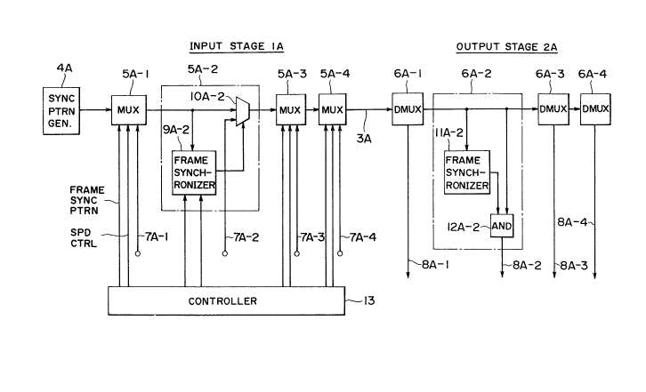
The embodiment of Fig. 1 is modified as shown in
Fig. 3 to implement a switching network for a time
division switching system. The switching network
comprises a frame sync pattern generator 4A identical to
the sync pattern generator 4 of Fig. 1, an input stage lA
connected to the sync pattern generator 4A and an output
stage 2A connected to the input stage lA by a link 3A.
Input stage lA comprises a plurality of cascaded LSI
multiplexers 5A-k each including a frame synchronzier
9A-k and a gate circuit lOA-k. Frame synchronizer 9A-k
compares each of the sync patterns Skj supplied from the
sync generator 4A with a frame sync pattern supplied from
a controller 13 to detect a match and generates a series
of slot timing pulses at intervals T to the control
terminal of gate circuit lOA-k. In the absence of the
slot timing pulses, the output of each preceding
multiplexer is passed through the multiplexer 5A-k to the
next and in the presence of the slot timing pulses data
bits Dki, which are supplied on input line 7A-k, are
passed to the next multiplexer. In this way, sync
patterns Skj from sync generator 4A are passed from one
multiplexer to the next and data bits Dji are multiplexed
into time slots uniquely associated with the sync pattern
supplied from the controller 13.
Output stage 2A comprises a plurality of LSI
demultiplexers 6A-k which are connected to channel 3A and
to which frame sync patterns Skj are respectively
assigned. Each demultiplexer 6A-k comprises a frame
synchronizer llA-k and an AND gate 12A-k . Frame
synchronizer llA-k compares the sync pattern Skj uniquely
assigned to it with each of the sync patterns Skj from
1~75~8
NE-116-MK
(099A/2) - 8 -
the input stage lA to enable the AND gate 12A-k at
intervals T to pass desired data bits to an output line
8A-k when a coincidence is detected by frame synchronizer
llA-k.
Assume that data bits on input line 7A-2 are to
be switched to output line 8A-2, controller 13 supplies a
sync pattern S2j to frame synchronizer 9A-2 so that data
bits from input line 7A-2 are multiplexed into time slots
t21, t22 and t23 (Fig. 2). Frame synchronizer llA-2
detects the assigned sync pattern S2j in the incoming
sync patterns and the multiplexed data bits are passed to
output line 8A-2. It will be seen that instead of
applying sync patterns to the input stage lA the
embodiment of Fig. 3 can be modified to apply sync
patterns from the controller 13 to the frame
synchronizers of output stage 2A by uniquely assigning
sync patterns Sjk respectively to the multiplexers of
input stage lA.
Details of the frame synchronizers 9A and 9B are
shown in Fig. 4. The synchronizer comprises a D
flip-flop 13 having a D input coupled to the output of
the preceding multiplexer and a clock input connected
from the carry output of a counter 17. The output of D
flip-flop 13 is connected to an exclusive-OR gate 14 to
which the frame sync pattern is supplied in serial form
from the control circuit 13. The output of exclusive-OR
gate 15 is applied to a 2-bit counter 15. Counter 15
enables an AND gate 16 if it receives a pulse from the
exclusive-OR gate 14 and disables it when it receives the
next pulse. When enabled, AND gate 16 allows clock
pulses from a clock source, not shown, to be supplied to
the counter 17. The binary outputs of counter 17 are
connected to an AND gate 18 with the exception that the
most significant bit is coupled by way of an AND gate 19
to which a speed control signal is applied from the
~X~7~68 71024-78
g
control circuit 13.
The synchronizer operates as follows. Initially,
the carry output of counter 17 is at logic zero and hence the
output of D flip-flop 13 is low. When a series of frame sync
pulses is supplied from the control circuit 13 to the
exclusive-OR gate 14, it switches to a logical one and causes
the output of counter 15 to enable the AND gate 16 to supply
clock pulses to the counter 17. The carry output goes high,
allowing the D flip-flop 13 to pass signals on the highway to
the exclusive-OR gate 14. If the output of D flip-flop 13
matches the sync pattern from control circuit 13, exclusive-OR
gate 14 produces a logical zero output. When a mismatch
occurs, an additional pulse will be supplied to counter 15 to
disable the AND gate 16 as an indication of an out-of-frame
sync, removing a clock pulse from the input of the counter 17.
If there is a match between the whole bits of the sync pattern
and the pulse input from the highway, exclusive-OR gate 14
remains in the logical-zero state. Counter 17 attains a pre-
determined count value when the whole bits of the sync pattern
have been supplied to the synchronizer. The carry output of
counter 17 goes low, preventing no further inputs from the
highway from entering the exclusive-OR gate 14 and resetting
the counter 15. The speed control command from control circuit
13 is at logical one during a low speed mode of operation, AND
gate 19 is enabled and all the inputs of AND gate 18 are at
logical one at the end of the frame sync pattern, providing a
C
12~7S68
71024-7
- 9a
gate timing pulse to the gate circuit lOA-k (lOB-k). During
a high speed mode of operation, the length of the sync pattern
is reduced to one half as much and the speed control command
is switched to logical zero, disabling AND gate 19. This
causes AND gate 18 to produce a gate timing pulse at one half
the intervals of the low speed mode.
The multiplexer/demultiplexer concept of the Fig.
~"'`,
1~75~i8
NE-115-~IK
(099A/2)
-- 10 --
1 embodiment can be advantageously incorporated into a
local area network as shown in Fig. 5. This local area
network comprises a frame sync generator 20 and a
plurality of cascaded switching nodes 21-k interconnected
by a network loop 22. Each switching node is implemented
by a high-speed LSI with a low level of integration.
Frame sync generator 20 generates the same frame sync
patterns as those shown in Fig. 2. Each switching node
21-k includes a receiver 23-k and a transmitter 24-k.
Receiver 23-k includes a frame synchronizer 25-k and an
AND gate 26-k. Similar to the previous embodiment, frame
sync patterns Skj are respectively assigned to frame
synchronizers 25-k. Synchronizers 25-k detect a match
with the corresponding frame sync patterns transmitted
from the preceding node 21-(k-1) and supplies a series of
slot timing pulses at intervals T to AND gate 26-k to
allow data bits destined to the own node to be passed
through gate 26-k to data output 27-k. Transmitter 23-k
comprises a frame synchronizer 30-k which is responsive
to a destination sync pattern Sdj supplied from an
address input 28-k. Frame synchronizer 30-k compares the
sync pattern Sdj with the sync patterns received from the
preceding node 21-(k-1) and detects a match. When this
occurs, it supplies a series of slot timing pulses at
intervals T to the control terminal of a gate circuit
31-k to multiplex data bits Dki into the time slots which
are uniquely assigned to the destination node.
Assume that switching takes place between nodes
21-2 and 21-3. Address input 28-2 supplies a sync
pattern S3j to the frame synchronizer 30-2, so that frame
synchronizer 30-2 detects a match with the sync pattern
S3j generated by the sync generator 20 and data bits D2i
are multiplexed by gate circuit 31-2 into the time slots
of the destination node 21-3. Therefore, the transmitted
data bits D2j are detected in the time slots of the node
1~7568
NE-116-MK
( 099A/2 ) - 11 -
21-3 and passed through AND gate 26-3 to data output
27-3. On the other hand, an address code S2j is supplied
from input 28-3 to frame synchronizer 30-3 of tranmitter
24-3 to multiplex data bits D3i into the time slots of
the node 21-2 and forwarded onto the network loop 22.
Frame synchronizer 25-2 of receiver 23-2 detects the
inserted sync pattern S2j to pass data D3j to data output
27-2.
An embodiment shown in Fig. 6 is a combination of
a slot interchange unit and the embodiment of Fig. 1 to
implement a switching network for time division switching
systems. The switching network comprises a multiplexer
stage connected in an inlet highway 30 and a
demultiplexer stage connected in an outlet highway 31,
the inlet and outlet highways being connected by a sync
slot interchange unit 32. The inlet highway 30 is
interposed by a plurality of multiplexers 33-k and the
outlet highway 31 is interposed by a plurality of
demultiplexers 34-k. A frame sync pattern generator 35
is connected to inlet highway 30 to supply a series of
frame sync patterns Skj at periodic intervals. Each
multiplexer 33-k has an input line 36-k connected to a
gate circuit 37-k to which the output of preceding
multiplexer 33-(k-1) is connected. Each multiplexer 33-2
includes a frame synchronizer 38-k to which the sync
pattern Skj is assigned. Frame synchronizer 38-k detects
a match between the assigned sync patterns and those
generated by the sync pattern generator 35 as in the
previous embodiments and supplies a series of slot timing
pulses at intervals T to the control terminal of gate
circuit 37-k, so that data bits Dki from input line 36-k
are multiplexed into the time slots assigned to the
multiplexer 33-k. As will be described hereinbelow, the
sync pattern assigned to a given input line is switched
to the time slot of a desired output line 39-k by the
~2~7S68
NE-116-MK
tO99A/2)
- 12 ~
slot interchange unit 32 and supplied to the outlet
highway 31. Each demultiplexer 34-k comprises a frame
synchronizer 40-k and an AND gate 41-k. Frame
synchronizer 39-k compares sync patterns Skj with the
corresponding sync patterns travelling through the outlet
highway 31 to detect a match. In response to the
detection of a match, a series of slot timing pulses is
supplied at intervals T from the synchronizer 40-k to the
AND gate 41-k to demultiplex the received data bits for
application to output line 39-k.
Referring to Fig. 7, the slot interchange unit 32
comprises a control memory 50 which normally stores sync
patterns in a predetermined order in a matrix array. A
write control circuit 51 transposes the stored sync
patterns in accordance with switching control signals.
Assume that data bits on input lines 36-2 and 36-4 are to
be switched to output lines 39-2 and 39-4, respectively,
and data bits on input lines 36-1 and 36-3 are to be
switched to output lines 39-1 and 39-3, respectively.
Write control circuit 51 transposes sync patterns S4j and
S2j on each row of the matrix. A frame synchronizer 52
is connected to the inlet highway 30 to detect the sync
patterns Skj and generates a timing signal. A read
control circuit 53 is associated with the control memory
53 to sequentially read out the contents of the memory
starting with the rightmost column of the first row in
response to a timing signal generated by synchronizer 52
in response to a series of sync patterns Sll, S21, S31
and S41 supplied from inlet highway 30. Read control
circuit 53 shifts the read address to the next row in
response to the arrival of a second series of sync
patterns S21, S22, S23 and S24. The timing signal from
frame synchronizer 52 is also supplied to the control
terminal of a switch 54. The output end of inlet highway
30 and the output of control memory 50 are connected to
75~8
NE-116-MK
(099A/2)
- 13 -
the inputs of switch 54. In the absence of timing signal
from frame synchronizer 52, sync patterns on inlet
highway 30 are applied to the outlet highway 31 and in
response to the presence of a timing signal from
synchronizer 52 the output of control memory 50 is
coupled to the outlet highway 31 to replace the original
sync patterns generated by sync pattern generator 35 with
the rearranged sync patterns.
With the sync patterns being rearranged on the
outlet highway 31, demultiplexer 34-4 is synchronized
with the transposed sync pattern S4j to pass data bits
D2i to output line 39-4 and demultiplexer 34-2 is
synchronized with the transposed sync pattern S2j to pass
data bits D4i to output line 39-2.
A modification of the time switch of Fig. 6 is
shown in Fig. 8. In the modified time switch, a frame
sync pattern generator 60 generates a single frame
pattern S instead of multiple patterns and a switching
C control unit 61 generates a slot position in~ Ll~ng
code. The time switch is essentially of a
multiplexer/demultiplexer configuration as in the Fig. 6
embodiment. The multiplexer stage of the time switch
comprises multiplexers 61-k cascaded in a highway 63 and
the demultiplexer stage comprises demultiplexers 64-k
cascaded in the highway 63. Each multiplexer 62k
includes a frame synchronizer 65-k, a slot position
detector 66-k and a gate circuit 67-k. Frame
synchronizer 65-k responds to the single frame pattern S
by supplying a timing pulse to a first input of the slot
position detector 66-k. Switching control circuit 61
supplies a slot position indicating code to the second
input of time slot position detector 66-k. In response
to it, slot position detector 66 k specifies the position
of a time slot with respect to the sync pattern S and
supplies a timing signal to gate circuit 67-k in a manner
12~7S~3
NE-116-MK
(099A/2) - 14 ~
as will be described later. In the absence of the timing
signal, a multiplexed data bit stream is passed through
gate circuit 67-k to the next multiplexer and in the
presence of timing signal, data bits from an input line
68-k are multiplexed into the specified time slot of the
bit stream and forwarded onto the highway 63.
Each of the demultiplexers 64-k comprises a frame
synchronizer 69-k, a slot position detector 70-k and an
AND gate 71-k. Synchronizer 69-k supplies a timing
signal to the slot position detector 70-k when it detects
the sync pattern S of the bit stream propagating through
the highway 63. Slot position detector 70-k, which is of
identical construction to the slot position detector
66-k, receives the same slot position indicating code as
supplied to slot position detector 66-k and specifies the
position of a time slot with respect to the sync pattern
S and opens the AND gate 71-k to demultiplex the data
bits in that time slot for application to an output line
72-k. It will be seen that time slot interchange occurs
between a multiplexer 62 and a demultiplexer 64 of a
desired set by applying the same control code to the slot
position detectors 66-k and 70-k from the control circuit
61.
Details of slot position detectors 66-k and 70-k
for a 16-time slot frame format are shown in Fig. 9.
Each slot position detector comprises a 4-bit counter 73
and a digital comparator 74. Counter 73 increments its
count in response to a slot timing pulse, initiates
counting in response to a timing pulse from the
associated frame synchronizer 65 or 69 and supplies a
4-bit count word to the digital comparator 74. The
switching control code from control circuit 61 is of a
4-bit word which is applied to the comparator 74 for
comparison with the 4-bit count value. A coincidence
pulse is generated from comparator 74 when the 4-bit
1~{~7S68
NE-116-MK
(099A/2) - 15 -
count value becomes equal to the 4-bit control code as an
indication of the timing at which the desired data bits
are to be extracted.
Returning to Fig. 8, if it is desired to switch
data bits from input line 68-1 to output line 72-1, the
control circuit 61 selects an idle time slot, say, T3 and
supplies the digital comparators 74 of slot position
detectors 66-1 and 70-2 with a 4-bit control code "0010"
indicating that the selected time slot T3 is displaced
two time slots with respect to the time slot Tl in which
sync pattern S is inserted. When two slot-timing pulses
are counted by counter 73, a coincidence pulse is
supplied from comparator 74 of slot position detector
66-1 to gate circuit 67-1 and data bits Dl from input
line 68-1 are multiplexed into time slot T3 of the bit
stream and forwarded through highway 63 to demultiplexer
64-2. Since the same "0010" code is supplied to the slot
position detector 70-2, an equality pulse is generated
from its comparator 74 exactly in time coincidence with
the time slot T3, so that data bits Dl are admitted
through AND gate 71-2 to output line 72-2.
The switching speed of the time switch of Fig. 9
can be advantageously doubled by including an AND gate 75
to the slot position detectors 66 and 70 as shown in Fig.
9. The most significant bit position of counter 73 is
connected to one input of AND gate 75, the second input
of AND gate 75 being connected to a dual mode port 76.
Controller 61 applies a ONE to port 76 when the system
operates in a low switching speed and applies a ZERO when
it operates in a high switching speed. If time slot T4
is to be selected during a low speed mode, switching
control bits "0100" are applied to ports B3 to B0,
respectively, with a ONE being applied to dual mode port
76. Comparator 74 produces an equality pulse Xl when the
counter 73 produces "0100" coincident with time slot T4.
~7568
NE-116-MK
(099A/2~
- 16 -
If time slots T4 and T12 are to be selected during a high
speed mode, the same switching control bits "0100" are
applied to ports B3 to B0 with a ZERO being applied to
dual mode port 76. Comparator 74 produces an equality
pulse X2 when counter 73 reaches "0100" coincident with
time slot T4 and produces an equality pulse X3 when it
reaches "1100" coincident with time slot T12.
The time switch of Fig. 8 can be advantageously
integrated with a space switch to form a combined time
space switching matrix as shown in Fig. 11. This time
space switching matrix generally comprises first and
second multiplexer stages 80 and 81 and first and second
demultiplexer stages 82 and 83. A space switch 84
provides interconnections between multiplexer stages 80
and 81 on the one hand and demultiplexer stages 82 and 83
on the other. Each of the multiplexer stages 80 and 81
is identical to the multiplexer stage of Fig. 7 and
likewise each of the demultiplexer stages 82 and 83 is
identical to the demultiplexer stage of Fig. 8.
Multiplexer stages 80 and 81 are connected to the space
switch 84 via inlet highways 85 and 86, respectively, and
demultiplexer stages 82 and 83 are connected to outlet
highways 87 and 88, respectively. Inlet highways 85 and
86 are selectively switched to outlet highways 87 and 88
when crosspoints a, b, c and d are selectively operated
in response to switching signals from a variable phase
pulsing circuit 89. Pulsing circuit 89 is responsive to
a control signal from switching controller 90 to generate
a switching pulse to any of the crosspoints of space
switch 84 in time coincidence with the time slot of
desired data bits on any of the inlet highways 85 and 86.
Therefore, data bits Dll on inlet highway 85 from an
input line 91-1 can be switched to an output line 94-3 by
applying a "0010" code to multiplexer 80-1 and
demultiplexer 83-3, for example, from controller 90 and
1~75~8
NE-116-MK
(099A/2) - 17 -
applying a switching pulse to crosspoint a from pulsing
circuit 89 in coincidence with time slot T3. At the same
time, a data packet D24 on inlet highway 86 from an input
line 92-3 can be switched through outlet highway 87 to an
output line 93-1 by applying a "0100" code to multiplexer
81-3 and demultiplexer 82~1, for example, from controller
90 and applying a switching with pulse to crosspoint d
from pulsing circuit 89 in coincidence with time slot T4.
Fig. 12 is a further modification of the time
switch of Fig. 6. The multiplexer stage of the time
switch comprises multiplexers 101-k connected in an inlet
highway 110 and the demultiplexer stage comprises
demultiplexers 102-k connected in an outlet highway 120
which is connected to the inlet highway 110 by a time
slot interchange unit 100. A controller 130 supplies
unique addresses Ak to the multiplexers 101-k and
demultiplexers 102-k, respectively. Each multiplexer
101-k multiplexes the unique address Ak with data bits Dk
from input line 103-k into predetermined time slots of a
frame. Each demultiplexer 102-k compares the unique
address Ak supplied from the controller with each of the
multiplexed addresses to detect a match and demultiplexes
the data bits identified by the matched address for
delivery to an output line 104-k.
As shown in Fig. 13, the slot interchange unit
100 comprises a control memory 105, a write control
circuit 106, a read control circuit 107 and a slot
selector 108. Control memory 105 stores addresses Ak.
Write control circuit 106 is controlled in response to a
switching control signal from controller 130 to transpose
the stored addresses in a manner similar to that
described with reference to Fig. 6. Read control circuit
107 provides read access to the control memory 105 in a
! sequential order at address timing. Slot selector 108
~X~75~8
NE-116-MK
(099A/2)
- 18 -
provides direct connection between the inlet and outlet
highways 110 and 120 in the absence of timing pulses from
controller 130 and switches its input to the output of
control memory 105 in response to slot timing pulses so
that the addresses Al to A4 multiplexed on the inlet
highway 110 as shown at 140 are replaced with the
transposed addresses as shown at 150. In the illustrated
example, addresses A2 and A4 are transposed and hence
data bits D2 and D4, which are identified by addresses A2
and A4 respectively on the inlet highway 110, are
identified by addresses A4 and A2 respectively on the
outlet highway 120. Due to the slot interchange, data
bits D4 and D2 are detected by demultiplexers 102-2 and
102-4 respectively, while data bits Dl and D3 are
detected by demultiplexers 102-1 and 102-3, respectively.
Fig. 14 is a modification of the local area
network of Fig. 5. In this modification, the transmitter
202-k of each switching node 201-k comprises a latch
203-k, an idle slot selector 204-k and a multiplexer
205-k. Multiplexer 205-k essentially comprises a memory
and a memory write control circuit. The output of
multiplexer 205-k is connected through a section of a
network loop 210 to the input of demultiplexer 209-(k+l)
and the output of the demultiplexer 209-k is connected to
the input of the multiplexer 205-k. As shown in Fig. 15,
the network generates a multiframe comprising n frames
each comprising (n + 1) time slots. The #l time slot of
each frame is used to carry the address of a destination
node the other time slots are used to carry data packets.
Latch 203-k stores the whole length of a multiframe
propagating through the network loop 210 to allow the
idle slot selector 204-k to select an idle address time
slot from address time slots 211-1 through 211-3. In
response to the selection of an idle time slot, it
supplies a binary code to the multiplexer 205-k
~2q7~68
NE-116-MK
(099A/2)
-- 19 --
representing the positions of the selected address time
slot and a set of data slots into which data packets are
to be multiplexed. The address slot of #n frame of a
each multiframe is associated with a set of #(n + 1) time
slots of each frame of that multifram. If the idle slot
selector 204-k selects the address slot of #n frame, it
specifies #(n + 1) time slots of each frame and generates
a binary code indicating the selected address time slot
#l of frame Fn and the specified data time slots ~(n + 1)
of frames Fl through Fn. The slot position indicating
binary code is applied to the multiplexer 205-k where the
address of a destination node and data packets are
received from the associated data terminal 212-k and
respectively multiplexed into the selected address time
slot and the specified data time slots.
The receiver 206-k of each node comp~ises a latch
207-k, an address detector 208-k and a demultiplexer
209-k. Unique address Ak is assigned to the address
detector 208-k. Latch 207-k stores the whole length of
each multiframe to allow the address detector 208-k to
detect a match between the assigned unique addresss Ak
and the destination address and supplies a slot position
binary code to the demultiplexer 209-k to demultiplex
data packets directed to the destination node.
If data terminal 212-1 wishes to communicate with
data terminal 212-2, it generates a destination address
A2. If all the address time slots are idle, the address
time slot #l of frame Fl will be selected and the
destination address A2 is multiplexed into the selected
address time slot and data packets Dll, D12 and D13 from
source terminal 212-1 are respectively multiplexed into
data slots #2 of frames Fl, F2 and F3. The multiplexed
address A2 is detected by address detector 208-2 of the
destination node 201-2 and a slot indicating binary code
is supplied to the demultiplexer 209-2, which
1~7568
NE-116-MK
(099A/2)
- 20 -
demultiplexes the data packets Dll, D12 and D13 from the
network loop 210 into the associated data terminal 212-2.
The foregoing description shows only preferred
embodiments of the present invention. Various
modifications are apparent to those skilled in the art
without departing from the scope of the present invention
which is only limited by the appended claims. Therefore,
the embodiments shown and described are only
illustrative, not restrictive.