Note: Descriptions are shown in the official language in which they were submitted.
~2g79~
SUPERCONDUCTI~G AL~!ERNAqrING li~INDING
CAPACI~O~ ELE~q?ROM~G~Eq!IC RE80~AT~:)R
Field of_the Invention
This application pertains to electromagnetic resonators
having a high quality fac~or "Q" at comparatively low frequen-
cies.
BackgroundQ f the Invention
The quality factor "Q" which characterizes the relative
damping of an electromagnetic resonator operating at its resonant
frequency is directly proportional to the energy stored by the
resonator and inversely proportional to the average power
dissipated in resiskive components of the resonator. The energy
stored by the resonator is in turn directly proportional to its
inductance. Accordingly, in order to increase the Q of an
electromagnetic resonator one may increase its inductance by
increasing the number of turns in inductors incorporated in the
resonator (the inductance of an inductor increases in proportion
to the square of the number of turns in the inductor); or, one
may decrease the resistance of the resonator. Unfortunately, if
the resonator inductance is increased by increasing the number
o~ inductor turns, there is a proportional increase of the
resonator resistance, due to the addition of resistive inductor
turn material. Similarly, if the resonator resistance is
decreased by removing resistive inductor turn material, then
there is a proportional decrease o~ the resonator inductance.
The result is that the resonator Q can be increased only
marginally by this technique.
The foregoing limitatlons are not of particular concern
~or resonators haviny high resonant frequencies, because the
resonator Q is also directly proportional to its resonant
frequency. However, at low resonant frequencies, such as the
audio ~requency range, the limitations aforesaid effectively
preclude construction o~ a high Q low frequency resonator.
- 1 - ~
7~iS
Typically, Q is very much less than 100 for an inexpensive audio
frequency resonator of practical si~e.
Recent advances in superconductor technology which have
dramatically elevated the minimum temperature at which certain
materials become superconductors (i.e. the minimum temperature
at which such materials have negligible resistance to the flow
of electric current) facilitate the construction o~ low cost,
high Q low freque~cy resonators. This is because the number of
turns o~ a resonator inductor may be increased, without yielding
a corresponding increase in khe resonator resistance if the
resistive components of the resonator are cooled to the minimum
temperature required for those elements to operate as supercon-
ductors. Because superconductors have negligible resistance, and
because the resonator Q is inversely proportional to its
resistance, very high resonator Q may be attained independently
of the resonator frequency. Even so, it would ordinarily be
necessary to separately construct the inductive and capacitive
components of the resonator with superconductor material and then
connect those components together with superconductor material.
The present invention greatly simplifies resonator construction
by facilitating formation of the capacitive and inductive
components as unitary superconductor material components.
Summary of the Invention
In its most general form, the invention provides an
electromagnetic resonator, comprising two or more non-intersect-
ing, substantially overlapping surfaces of approximately similar
size and shape. The surfaces are separated from one another by
a distance which is small in comparison with physical extent of
the surfaces. one or more substantially non-intersecting,
electrically conductive paths cover substantial portions of each
of the surfaces. The widths of the conductive paths are
substantially smaller than the physical extent of the surfaces.
No conductive path on any one of the surfaces is electri.cally
connected to a conductive path on any of the other surfaces. The
conductive paths are oriented such that, for each of the
- 2 -
~29~9SS
surfaces, "macroscopic current" (hereinafter defined) flows, with
respect to the surfaces, in a direction other than the direction
in which "microscopic current" (hereinafter defined) flows in the
paths. The conductive paths are further oriented such that the
electromagnetic resonator supports at least one mode of electro-
magnetic oscillation between a first state in which the electro-
magnetic energy stored by the resonator is substantially
electrostatic energy, and a second state in which the electromag-
netic energy stored by the xesonator is substantially magneto-
static energy; the frequency of such oscillation being sub~tan-
tially lower than any characteristic self-resonant fre~uency of
electromagnetic oscillation of any one of the paths, taken alone.
The invention further provides an electromagnetic
resonator as described above, further comprising first and second
electrical conductors respectively traversing non-intersecting
paths which conform, respectively, to first and second surfaces.
The surfaces and the conductors are separated by a distance "t",
such that, over a substantial portion of the region between the
surfaces:
(a) t << Rl, where R1 is the radius of curvature of the
first surface at a selected point;
(b) t << R2, where R2 is the radius of curvature of the
second surface at a point on the second surface
intersected by a vector normal to the first surface at
the selected point;
(c) t > 0;
(d) t is measured along the aforementioned vector;
and,
(e) t is much less than the physical extent of either of
the surfaces.
If the end point~ of the first conductor are defined as "al" and
"bl" respectivel~, then the analogous end points "a2" and "b2" of
the second conductor are defined as those points on the second
conductor which, when oppositely charged and having a continuous
charge distribution therebetween, produce an electric field
7~55
distribution, in regions away from the surfaces, which is more
similar to the electric field distribution produced, in regions
away ~rom the surfaces, by a charge distribution similarly
applied to the first conductor than would be the case i-f the end
points a2 and b2 were interchanged. The conductors are con-
figured and positioned relative to one another such that if
current flow from a1 to b~ produces a magnetic field distribution
B1(x,y,z); and, current flow from b2 to a2 produces a magnetic
~ield distribution B2(x,y,z); then Bl(x,y,z) and B2(x,y,z) are
substantially similar, in the sense that a coefficient "C"
defined as C = ~B1(x,y,z)-B2(x,y,z)dxdydz has the property that
C > O.
The invention further provides an electromagnetic
resonator of the general type first described above wherein the
conductive paths are further oriented such that current flow
throuyh the paths on one of the resonator surfaces, in a
direction which transports charge toward the centre of that
surface, produces a magnetic field distribution B1(x,y,z), and
current flow through the paths on one of the resonator surfaces
adjacent said one sur~ace, in a direction which transports charge
away from the center of said adjacent surface, produces a
magnetic field distribution B2(x,y,z), where B1(x,y,z) and
B2(x,y,z) are substantially similar in the sense that a coeffi-
cient ~ICII defined as C = ~JB1 (x,y,z)-B2(x,y,z~dxdydz has the
property that C > 0.
Advantageously, the surfaces may be spiral rolls. The
conductive paths may advantageously take the form of spirals when
the resonator sur~aces are laid flat. Preferably, the surfaces
are spiral rolls and the conductive paths take the form of
spirals when the surfaces are unrolled and laid flat.
The surfaces may also be discs, and the conductive
paths may be spirals on the disc surfaces. Alternatively, the
surfaces may be spiral rolls and the conductive paths may be
substantially parallel to one another on each of the surfaces.
~2~95~i
As a further alternative, the surfaces may be spiral rolls; and,
on one side of each of the surfaces, the paths may take the Eorm
of spirals when the surfaces are unrolled and laid flat; and, on
the opposite side of the surfaces, the paths may be substantially
parallel to one another.
In an~ embodiment of the invention the conductive paths
are adYantageously formed o~ superconductor material; preferably,
thin film, high temperature superconductor material.
It will be practically advantageous to construct
resonators of the general type first descri~ed a~ove in which the
resonator surfaces are substantially planar and are separated by
a substantially constant displacement over the region between the
surfaces. For example, the opposed flat surfaces of a disc-
shaped insulator may serve as the first and second surfaces, in
which case the first and second conductors may be oppositely
directed spirals placed, respectively, on the first and second
insulator disc surfaces. More particularly, the invention also
provides an electromagnetic resonator comprising an electrical
insulator having opposed first and second sides. A first
electrical conductor which spirals in a first direction is placed
on the first side of the insulator. A second electrical
conductor which spirals in a second direction opposite to the
first direction is placed on the second side of the insulator.
The spiral conductors are configured such that current flow
through the first conductor, in a direction which transports
charge toward the centre of the flrst conductor spiral produces
a magnetic field distribution B1(x,y,z), and current flow through
the second conductor, in a direction which transports charge away
from the centre of the second conductor spiral produces a
magnetic field distribution B2~x,y,z), where B1(x,y,z) and
B2(x,y,z) are substantially similar in the sense that a coeffi-
cient "C" defined as C = rr~Bl(x,y,z)-B2(x,y,z)dxdydz has the
property that C > O.
-- 5 --
~79~
The invention ~urther provides an electromagnetic
resonator oP the ~eneral type first described above, and Purther
comprising a plurality o~ electrical insulators stacked atop one
another. Every second one of the insulators in this stacked
embodiment is an electromagnetic resonator functionally identical
to the resonators described in the immediately preceding para-
graph.
The conductors need not be affixed to the insulator
surfaces. They need only traverse non self-intersecting paths
which conform to surfaces having the characteristics set forth
in the foregoing description of the general form of the inven-
tion. Thus, in yet another embodiment, the invention provides
an electromagnetic resonator comprising a plurality of "n" elec-
trical insulators stacked atop one another. An electricalconductor which spirals in a Pirst direction is placed between
each pair oP insulators "i" and "i~l", where:
(i) i = 1, 3, 5, 7, ... n-2 i~ "n" is an odd number; and,
(ii) i = 1, 3, 5, 7, ... n-1 if "n" is an even number.
Another electrical conductor which spirals in a second direction
opposite to the first direction is placed between each successive
insulator pair "i+l" and "i+2", where:
(i) i = 1, 3, 5, 7, ... n-2 if "n" is an odd number; and,
(ii) i = 1, 3, 5, 7, ... n-3 iP "n" is an even number.
Here again, the conductors are configured and positioned relative
to one another such that current Plow through each oP the
conductors positioned between each pair of insulators "i" and
~ 1", in a direction which transports charge toward the centre
oP the conductor spirals produces a magnetic field ~istribution
-
Bl(x,y,z), and current ~low through each o~ the conductors
between the successive pairs of insulators "i~l" and "i-~2", in
- 6 -
~L297~5S
a direction which transports charge away ~rom tha centre of the
successive insula~or pair conductor spirals produces a magnetic
field distribution B2(x,y,z), where B~(x,y,z) and B2(x,y,z) are
substantially similar in the sense that a coefficient "C" defined
as C = ~rrB1(x,yl~) B2(x,y,z)dxdydz has the property that C > 0.
The invention further provides a method of making an
electromagnetic resonator in which spiral-shaped electrical
conductors are applied to the surfaces of one or more planar
insulators, such that conductors on one side of each of the
insulators spiral in a first direction, and conductors on the
opposed sides of each of the insulators spiral in a second
direction opposite to the first direction. The insulators are
then stacked atop one another.
The invention further provides a method of making an
electromagnetic resonator in which electrical conductors are
applied diagonally across the surfaces o~ two or more planar
insulators. The insulators are placed atop one another such that
conductors on adjacent surfaces of the insulators lie in
different directions. The insulators are then rolled to~ether
to form a spiral roll.
The invention also provides a method of making an
electromagnetic resonator in which an electrical conductor is
applied to a surface of a first planar insulator, such that the
conductor extends around the outer region of the insulator
surface in spiral fashion. A plurality of discrete electrical
conductor segments are applied to the corresponding outer region
of a surface of a second planar insulator. The first and second
insulators are then placed atop one another, such that conductors
on adjacent surfaces of the in5ulators line in different
directions. ~he insulators are then rolled together to form a
spiral roll.
~297~15~
srief_Des_rip~ion Q~ the Drawings
Figure 1 depicts a plurality of non-intersecting,
substantially overlapping surfacQs capable of defining a
generaliæed electromagnetic resonator in accordance with the
invention.
Figure 2 illustrates one of the surfaces o~ Figure 1,
having a plurality of substantially non-intersecting, electrical-
ly conductive paths covering a substantial portion of the
surface.
Figure 3 is an oblique perspective view of an electro-
magnetic resonator constructed in accordance with one embodiment
of the invention.
Figure 4 is a side elevation view of an electromagnetic
resonator in accordance with another embodiment of the invention;
the vertical dimension being greatly exaggerated in comparison
to the horizontal dimension.
Figure 5 is a top elevation view of the electromagnetic
resonator of Figure 4; hidden lines being used to illustrate the
conductor spiral on the side of the resonator which is beneath
the plane of the paper; and the displacement between radially
adjacent segments o~ each of the conductors being greatly
exaggerated in comparison to the displacement across a single
segment of either conductor.
Figure 6 is a side elevation view of a "stacked"
electromagnetic resonator in accordance with another embodiment
of the invention.
Figure 7 is similar to Figure 5, but shows only the
conductor spiral on the insulator surface which is above the
plane of the paper.
~2~5~
Figure 8 is a side elevation view of a p~rtion of the
electromagnetic resonator of Figure 6; the vertical dimension in
Figure 8 being greatly exaggerated in comparison to the horizon-
tal dimension.
Figure 9 is a circuit schematic diagram of a lumped
components model of the invention.
Figure 10 is an oblique perspective view of an
alternative embodiment of the invantion showing a spiral
conductive path on one surface of the resonator and a plurality
of discrete radial conductive paths on an adjacent sur~ace of
the resonator.
Figure 11 illustrates another embodiment of the
invention consisting of two conductive path-bearing planar
insulators (portions of which are depicted in Figures ll(b) and
ll(c) respectively) laid atop one another and rolled together to
form a spiral roll as shown in Figure ll(a).
Figure 12 depicts another embodiment of the invention
in which planar insulators (portions of which are depicted in
Figures 12(b) and 12(c) respectively) having a different pattern
of conductive paths are rolled together to form a spiral roll as
shown in Figure 12(a).
Detailed Description of the Preferred Embodiments
~o assist those skilled in the art, certain geometrical
relationships will first be defined. Electromagnetic resonators
constructed in accordance with the invention incorporate two or
more non-intersecting, substantially overlapping surfaces of
approximately similar size and shape which are separated ~rom one
another by a distance which is small in comparison to the
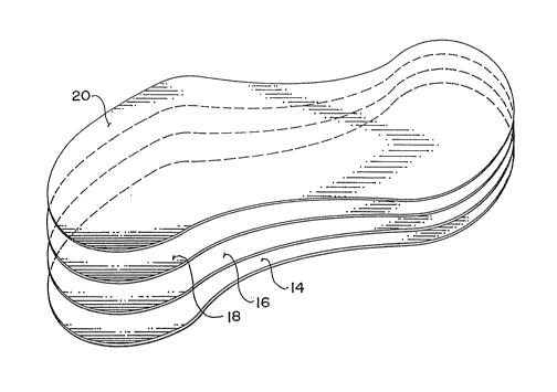
physical extent of the surfaces. Figure 1 illustrates four such
surfac,es 14, 16, 18 and 20. Surface 20 is further depicted in
Figure 2, which also illustrates a thin film structure 22 applied
9~
to surface 20. Structure 22 incorporates a number of non--
intersecting, electrically conductive paths 24, 26 and 28 which
cover a substantial portion of surface 20 (the paths may be
applied directly to surface 20, but the use of thin film path-
bearing structures is considered to be practically convenient).The width of each of paths 24, 26 and 2~ is substantially smaller
than the physical extent of surface 20. Similar conductive path-
bearing structures ~not shown) are provided on each of surfaces
14, 16 and 18. No conductive path on any one o~ the surfaces is
lo electrically connectsd to a conductive path on any of the other
surfaces.
There are an infinite number of widely differing
surfaces, structures and paths having characteristics of the sort
described in the preceding paragraph. The present invention is
directed to a particular subset of such structures having
particularly useful electromagnetic characteristics. To assist
those skilled in the art in comprehending this subset, it is
useful to develop the concept of "macroscopic" and "microscopic"
currents.
If surfaces 14, 16, 18 and 20 of Figure 1 each bear a
conductive structure such as structure 22 depicted in Figure 2l
it will be realized that the group of conductive structure-
bearing surfaces as a whole has a siynificant similarity to a
parallel plate capacitor, in which substantially equal but
opposite surface charge densities exist on adjacent regions of
the conductive structures. In relation to conventional capaci-
tors which are incorporated in a resonant circuit, and also in
relation to the conductive structures contemplated by the present
invention, it is meaning~ul to discuss the change o~ distribution
of surface charge in a macroscopic sense, and to define "macro-
scopic current" as the yradient of the time derivative of the
macroscopic sur~ace charge distribution. Consider for example
Figure 3, which illustrates a resonator comprising circular
surfaces 32, 34 and 36 to which spiral shaped conductive
structures 33, 35 and 37 are respectively applied. It will be
-- 10 --
~s~ss~
noted that sp.irals 33 and 37 spiral outwardly in a clockwise
direction from the centre of surfaces 32 and 36 respectively,
whereas spiral 35 spirals outwardly in a counterclockwise
direction from the centre of surface 34. Those skilled in the
art will accordingly appreciate that the mode of oscillation of
electromagnetic energy in these spirals consists of an alteration
~rom a state in which the central regions of the two clockwise
spirals 33, 37 are predominantly positively charged, with their
respective peripheral regions negatively charged, and the
lo opposite situation prevailing on the counterclockwise spiral 35
(namely, the central region of the counterclockwi.se spiral 35 is
predominantly negatively charged, and the peripheral reg.ion of
the counterclockwise spiral 35 is predominantly positively
charged); to a state in which the central regions of the two
clockwise spirals 33, 37 are predominantly negatively charged,
with their respective peripheral regions positively charged, and
the opposite situation prevailing on the counterclockwise spiral
(i.e. the central region of spiral 35 is predominantly
positively charged, and the peripheral region of spiral 35 is
predominantly negatively charged). In this situation, the
"macroscopic currents" in the conductive structures are directed
radially inwardly and outwardly as the oscillation occurs. This
oscillation is hereinafter described in greater detail, but at
the moment the important concept to note is that for a given
conductive structure and a given mode of oscillation, there is
a well defined macroscopic current distribution which reflects
the overall macroscopic flow of charge in the structure.
The actual or "microscopic" electric current which
flows as charge moves ~rom one region o~ any conductive structure
to another must of course follow the physical conductive paths
which make up the conductive structure. The actual "microscopic"
flow of electric current in any given region of the conductive
structure may be in a direction which is substantially different
from the direction o~ overall macroscopic current ~low and may
be substantially greater than the magnitude of the macroscopic
;5
current flow. The present invention exploits this difference
between macroscopic and microscopic curren~s.
Since the macroscopic charge densities of vertically
adjacent regions of conductive structures 33, 35 and 37 depicted
in Figure 3 are essentially equal and opposite, it is in general
true that the macroscopic currents occurring within adjacent
conductive structures tend to be substantially squal and
opposite. Equal and opposite surface currents produce relatively
little magnetic field energy. However this is irrelevant for
present purposes because the currents which are actually
responsible for creating magnetic fields are the actual micro-
scopic currents which flow in the conductive structures. The
present invention recognizes that it is possible to structure
the shape of the conductive paths on adjacent resonator surfaces
in such a manner that the microscopic currents are not substan-
tially equal and opposite on adjacent surfaces of the resonator
and are accordingly capable of produciny magnetic fields which
are additive and which extend through a significant volumetric
region. This results in a resonator having a high capacitance,
high inductance characteristic which enables electromagnetic
oscillation to occur at a comparatively low frequency. Since an
arbitrary conductive structure will have a natural self-resonant
frequency determined by its self-inductance and self-capacitance,
a structure having the aforementioned high capacitance, high
inductance characteristic can be defined as one whose resulting
electromagnetic resonance is substantially lower in frequency
than any characteristic self-resonant frequency of electromag-
netic oscillation of any one of the conductive paths incorporated
in the structure, taken alone.
The nature of the eleatromagnetic oscillation herein
contemplated consists of alterations from a state in which the
electromagnetic energy is primarily electrostatic energy stored
substantially between the resonator surfaces, to a state in which
the electromagnetic energy is primarily magnetostatic energy.
- 12 -
7~S5
Although the embodiment depicted in Figure 3 shows only
three spirals, any number of spirals greater than one may be
employed to construct an electromagnetic resonator in accordance
with the invention. The spirals on adjacent surfaces alternate
from clockwise ~o counterclockwise as depicted in Figure 3. This
results in microscopic currents which at any given time flow in
the same direction. At the heginning of the electromagnetic
oscillation cycle, there are essentiall~ no currents and
essentially all of the resonator's electromagnetic energy takes
the form of electrostatic energy stored between the resonator
surfaces, corresponding to the fields resulting from a charga
distribution which is predominantly positive in the center and
negative in the periphery of the clockwise spirals 33, 37; and
the opposite (i.e. negative centre and positive periphery) for
the counterclockwise spiral 35. As the oscillation cycle
progresses, this charge distribution is reduced and then built
up in the opposite sense, as a result of macroscopic current
flows which are radial and opposike on adjacent resonator
surfaces. Despite the fact that the macroscopic currents on
adjacent resonator surfaces oppose one another, the fact that
adjacent resonator surfaces have an alternating sense of spiral
causes the corresponding microscopic currents to be entirely in
the clockwise direction during the first half of the oscillation
cycle. As a result, large scale strong magnetic fields are
created, predominantly in a direction perpendicular to the
spirals. Midway through the oscillation process, the charge
distribution in the resonator is neutralized, but there is an
intense magnetic field, so that most of the energy is electromag-
netic at this point. Then, the opposite electrostatic end of the
oscillation cycle is reached, as the currents drop to zero and
most of the resonator's electromagnetic energy again takes the
~orm of electrostatic energy stored between the resonator
surfaces, but with a charge distribution precisely opposite to
that which prevailed when the oscillation cycle began. The
second half of the oscillation cycle is the precise inverse of
the first hal~ and the cycle is then complete. As may be seen,
the essence of the invention lies in the fact that the orienta-
- 13 -
~2~t7~S~i
tion of the resonator's conductive paths cau6e the microscopic
curren~s to be additive even as the macroscopic currents are
equal and opposite in response to the capacitive interaction o~
the conductive structuras.
There are many alternative ways of constructing a
resonator ha~ing the general oscillation characteristics
described above. For example, spiral conductive structures can
be formed on disc-shaped insulators by means of printed circuit,
thin film or integrated circuit fabrication techni~ues. One
approach would be to deposit spiral conductors on opposed
surfaces o~ insulators and then separate the spiral-bearing
insulators from one another with insulators having no conductors.
The spiral conductive structures need not be physically connected
to the insulators, although it may be useful to employ some form
of connection in constructing electromagnetic resonators in
accordance with the invention.
An important advantage o~ the invention is that there
exist techniques for making very thin insulators with very finely
detailed conductive paths. Accordingly, it is possible to have
a great deal of capacitance present (due to large number of
surfaces which can be placed in a small volume) and a large
amount of inductance present (due to large relative lengths of
the conductive paths in question) so the frequency of oscillation
can be very low. In general, one would expect a relatively low
Q to result, due to the high resistance to current flow in such
a fine structure. This can however be overcome by forming the
conductive paths with superconducting material, more particular-
ly, thin film, high temperature superconducting material.
Figures 4 and 5 illustrate an electromagnetic resonator
50 according to a first preferred embodiment of the invention.
Resonator 50 comprises an electrical insulator 52 ha~ing opposed
first and second sides 52, 56. A first electrical conductor 58
(preferably, but not necessarily, formed of superconductor
material) which spirals outwardly from the centre of insulator
- 14 -
912~ 9SS
52 in a first direction (which happens to be clockwise, as
illustrated in Figure 5), is etched or bonded onto insulator
first side 54; for example, using printed circuit, thin film or
integrated circuit fabrication techniques, depending upon the
dasired degree of miniaturization of the conductors. A second
electrical conductor ~0 (also preferably, but not necessarily,
formed o~ superconductor material) which spirals outwardly from
the centre of insulator 52 in a second direction opposite to the
first direction aforesaid (the "second" direction happens to be
counterclockwise, as illustrated in Figure 5, because the "fi~st"
direction is clockwise in the example of Figure 5) is similarly
etched or bonded onto insulator second side 56. Spiral conduc-
tors 58, 60 are in all respects identical, except they spiral in
opposite directions.
current which is induced to flow through first
conductor 58, in a direction which transports charge toward the
centre of the first conductor spiral produces a magnetic field
distribution which is defined as B1(x,y,z). Current induced to
flow through second conductor 60, in a direction which transports
charge away from the centre of the second conductor spiral pro-
duces a magnetic field distribution which is defined as
B2(x,y,z). Because conductors 58, 60 are identical, excepting
their opposite spirals, and because they are positioned vertical-
ly adjacent one another on opposite sides 54, 56 of insulator 52,
Bl(x,y,z) is substantially similar to B2~x,y,z), in the sense
that a coupling coefficient "C" defined as C
~JB1(XIYIZ) B2(XIYIZ) dxdydz has the property that C > 0.
Although not essential, it will be preferable and
practically advantageous, in order to facilitate simplified
construction of inexpensive resonators, to ensure that the
displacement ~t" between insulator sides 54, 56 is substantially
constant. It will also be advantageous to ensure that insulator
sides 54, 56 are substantially planar, although this is not
; essential; for example, the insulator may be a cylinder, or it
may have other arbitrary curvature. It will also be practically
- 15 -
~l~97~5~3;
advantageous to form insulator 52 as a disc as shown in Figure
5, although this is not essential either - insulator 52 may have
any desired shape. Moreover, it is not essential that conductor
spirals 52, 60 he centred with respect to insulator 52 (although
it is important to ensure that the spirals are sufficiently well
centred with respect to one another to ensure substantial
similarity of the magnetic field distributions as aforesaid).
Similarly, spiral conductors 58, 60 need not extend from the
outer rim of insulator 52 to the centre of insulator 52 - the
conductors may stop short of the rim and/or the centre of
insulator 52.
Generally, one need only provide first and second
electrical conductors which traverse non self-intersecting paths
which conform, respectively, to first and second surfaces, such
that the surfaces and the conductors are separated by a distance
"t" > o. Over a substantial portion of the region between the
surfaces, t should have the following characteristics: t << R1,
where R1 is the radius of curvature of the first surface at a
selected point (throughout this application, the phrase "radius
of curvature" of a surface is used to mean the smallest of the
radii of curvature, at any particular point on the surface, of
the family of curves formed by intersections of the surface with
the family of planes which contain a vector normal to the surface
at the particular point): t ~< R2, where R2 is the radius of
curvature of the second surface at a point on the second surface
intersected by a vector normal to the first surface at said
selected point; t is measured along said vector: and, t is much
less than the physical extent of either of the surfaces. The end
points of the first conductor are defined as "al" and "bl"
respectively. The analogous end points "a2" and "b2" of the
second conductor are defined as those points on the second
conductor which, when oppositely charged and having a continuous
charge distribution therebetween, produce an electric field
distribution, in regions away from the surfaces, which is more
similar to the electric field distribution produced, in regions
away from the surfaces, by a charge distribution similarly
- 16 -
~L29~9S~
applied to the first conductor, than would be the ~ase if the
end points a2 and b2 were interchanged. The conductors are
configured and positioned so that current flow from at to b1
produces a magnetic ~ield distribution B1(x,y,z); and, curxent
flow from b2 to a2 produces a magnetic field distribution
B2(x,y,z); where Bl(x,y,z) and B2(x,y,z) are substantially similar
in the sense that a coef~icient "C" defined as C
J~B1 (x,y,z) B2(x,y,z)dxdydz has the property that C > 0.
Figure 6 illustrates second and third embodiments of
the invention, both o~ which contemplate a plurality of "n"
electrical insulators stacked atop one another. For ease of
re~erence, Figure 6 shows an insulator stack 70, comprising
insulators labelled "1", "2", "3", ... "n-2", "n-l", "n". Spiral
conductors are located between successive inductor pairs as
hereinafter described. In the second embodiment of the inven-
tion, insulators having electrically conductive spirals etched
or honded thereon as described above with reference to Figures
~ and 5 are alternated in stack 70 with insulators having no
conductors. In the third embodiment of the invention, none of
the insulators in stack 70 have conductors etched or bonded onto
them as in the first and second embodiments; instead, discrete
spiral conductors are placed between adjacent insulators in the
manner hereina~ter explained.
Dealing first with the second embodiment o~ the
invention, every second one of the insulators in stack 70 is
identical to electromagnetic resonator 50 described above with
re~erence to Figures ~ and 5~ That is, every second one of the
insulators in stack 70 has ~irst and second oppositely directed
spiral conductors on opposed sides thereof. Insulators having
no conductors are positioned between each of the conductor--
bearing insulators to form stack 70. The number of insulators
"n" in stack 70 may be odd or even. Moreover, the conductor-
bearing insulators within stack 70 may be either the odd or theeven numbered insulators.
~7~i5
In the third embodiment, none of the insula~ors
comprising stack 70 have conductors etched or bonded onto them.
Instead, discrete conductor spirals (which may for example be
thin film conductors on insulating thin film substrates, or wafer
thin conductors without substrates) are placed between adjacent
insulators to duplicate the characteristics of a stack con-
structed in accordance with the second embodiment o~ the
invention. More particularly, an electrical conductor which
spirals in a first direction is plaeed between each pair of
insulators "i" and "i+1" in stack 70. If the total number of
insulators "n" in stack 70 is an odd number, then i = 1, 3, 5,
7, ... n-2. If "n" is an even number, then i = 1, 3, 5, 7, ...
n-1. An electrical conductor spiralling in a second direction
opposite to the first direction is positioned between each
successive insulator pair "i+l" and "i+2". For the conductors
placed between the successive insulator pairs, i = 1, 3, 5, 7,
... n-2 if the total number of insulators "n" in stack 70 is an
odd number; or, i = 1, 3, 5, 7, ... n-3 if "n" is an even number.
The oppositely spiralling conductors are so configured and
positioned that current which is induced to flow through each of
the conductors between each pair o~ insulators "i" and "i+1", in
a direction which transports charge toward the centre of the
conductor spirals produces a magnetie field distribution defined
as B1(x,y,z), and current induced to flow through each of the
conductors between the successive pairs of insulators "i~l" and
~ 2", in a direction which transports charge away ~rom the
centre of the successive insulator pair conduetor spirals
produces a magnetic field distribution defined as B2(x,y,z), such
that Bl(x,y,z) is substantially similar to B2(x,y,z) in the sense
that a coupling coefficient "C" defined as C
~B1(x,y,z) B2(x,y,z)dxdydz has the property that C > 0.
Advantageously, the resonator is encapsulated in a
dieleetric material to minimize mechanical vibration of the
conductors
3L29?795~
A simplified mathematical analysis of the invenkion is
now presented. ~he analysis is similar in nature to the precise
calculations that would be applicable to any given embodiment
of the invention, which in general would have to be performed
numerically.
The analysis pertains to a stack of resonators
constructed in accordance with the second or third embodiments
of the invention. The following assumptions are made with
reference to Figures 7 and 8:
Let: w = the displacement between the centres of radially
adjacent segments of a given conductor spiral.
g = the displacement between adjacent edges of
radially adjacent segments of a given conductor
spiral.
2d = the thickness of one spiral conductor-bearing
insulatorplus one non conductor-bearing insulator
~in the second embodiment); or, the thickness of
two non conductor-bearing insulators plus the
thickness of conductor spirals placed on opposite
sides of one of those insulators (in the third
embodiment).
L = the height of the insulator stack.
nL = the number of conductors in the stack.
r = the radius of a disc-shaped insulator (which
therefore has surface area A = ~r2).
~0 = the permittivity of free space.
er = the relative permittivity o~ the insulator
dielectric material.
= the permeability constant.
nO = r/w = the number of spiral turns per conductor.
Let there be a peripheral region defined to be the
35 region outside a circle of radius = ~r.
-- 19 --
1~7~ iS
Although the ~ollowing assumptions are not essential
for resonance to occur, they facilitate derivation of the typical
fraquency of operation of the device. Hence, assume:
1. The insulators are disc-shaped.
2. The conductor spirals are tightly packed and cover
substantially all of the insulator sur~aces.
3. g << w.
4. d ~ t.
For analytical purposes the resonator may be viewed as
consisting of lumped inductances and capacitances, even though
such inductances and capacitances coexist intimately with one
another in the actual resonator. Such treatment is common in
circuit analysis, and generally yields a reasonable approxima-
tion, provided that the wavelengths associated with the electro-
magnetic oscillations are large compared to the physical extentof the device. For example, it is not unusual in conventional
circuit analysis to view a real inductor as a combination of an
ideal inductor connected in parallel with a small capacitor
(which represents the capacitance between the inductor windings)
and connected in series with a resistor (which represents the
resistance of the inductor windings).
In the present oase, such a lumped components model can
be made by considering the mode of electromagnetic oscillation
of the resonator. As with most electromagnetic resonators, the
electromagnetic energy in the oscillation alternates between
states o~ predominantly electric ~ield energy and states of
predominantly magnetic field energy. In the present resonator
these are states where, ~irst, most o~ the electromagnetic energy
is in an electric ~ield between adjacent conductors, that field
being perpendicular to and primarily confined between the
surfaces to which those conductors con~orm; and, second, where
- 20 -
the energy is predominantly in a magnetic field which is also
perpendicular to the surfaces to which the conductor paths
conform, but which extends signi~icantly throughout the resona-
tor, beyond the region between the surfaces to which any two
adjacent inductors conform, so that the magnetic field lines are
shared by several conductors. In terms of the motion of charye,
the resonator alternates between a state in which the peripheral
regions of a given conductor are charged oppositely to the
central region of that conductor and also oppositely to the
peripheral regions of the immediately adjacent conductor(s); and
a state in which opposite charges prevail in each of those
regions. In the oscillation between these two states, there are
current ~lows on the spiral conductors, with all such flows
producing magnetic fields which add to one another. A convenient
way o~ viewing this oscillation is to think of a plane midway
between each pair of adjacent conductors as a plane of zero
electrical potential.
From this point of view, each conductor can be viewed
as the equivalent of the lumped circuit shown in Figure 9, where
the ground symbols represent zero potential points. The two
capacitances correspond respectively to the inner and outer 50%
of the area of the disc, where the capacitance is between the
conductor in these two regions and the plane of zero electrical
potential. The e~fective lumped inductance is of course caused
by the turns of the spiral conductor. We can now proceed with
calculation of the resonant requency, bearing in mind that this
is an approximate treatment only. Two cases are analyzed; one
in which the product nLd is very much greater than r; the other
in which nLd is very much less than r.
Consider ~irst the case in which nLd is very much
greater than r. For a general parallel plate capacitor it is
known that C = (FC606rAc)/dc, where Ac is the plate area, dc is the
plate separation and Fc is a geometric factor o~ order 1. Since
the plane of zero potential in this model is midway between the
conductor plates, we have dc ~ d/2. Since each capacitor
- 21 -
~79~i5
occupies half the disc area, we have Ac = ~(~r2). Therefore,
CO = C; = Fc~O~r~r2/d. Intuitively, a reasonable guess for Fc in
this situation might be approximately ~, multiplied by 2 to take
into account the fact that each plate "sees" two adjacent zero
poten~ial surfaces. Therefore Fc is about 1. Accordingly,
CO = C; = ~0~,7rr2/d.
If q(t) is the excess positive charge resident in the
peripheral region of the conductor at any time, then -q(t) is the
complimentary charge in the inner region of that conductor. By
the definition of capacitance, then,
VO = q/CO = q/(FC~O~r~r /d)
If we define the voltage across the inductor to be
VL = VO - Vi, we have therefore:
VL = (2/~)(1/(FC~O~r))((d/r2)q)
( 2/71 ) ( ~ o~r) ) ( (d/r2) q)
VL must also equal the rate of change of magnetic flux
in the inductor: VL = ~. To calculate ~, we must assume that all
conductor layers are oscillating in the same manner in phase,
which will be found to be a self-consistent assumption. Assuming
25 also that nLd >> r, we employ the formula for the magnetic field
of a solenoid. Further, let us model the actual winding to
consist o~ n~/2 turns at a radius of ~r, which is the boundary
between CO and Ci. Here we can use the formula:
Bu = FL~o(NI)/L
where the sign takes into accounk Lens' law, and where N is the
total number of turns (in this case N=nLn~), I is the current (in
this case ~(t)), L is the length (in this case nLd), and FL iS a
geometric factor of order 1 (in this case approximately 1 seems
a yood intuitive guess).
'795~;
Further, the flux in this coil is simply ~ = BAn~/2,
since we ha~e modelled the number of turns to be n8/2. There-
~ore:
VL = ~L
= ((-~r ) ~118) FL~O ( (nLn~/ (nLd) ) q(t~
) FL~O (n~3/d)q(t)
~ O(n92/d)q(t)
And, noting that the two equations for VL must be equal:
(2/~)(l/~0~r)(d/r2)q = -((~ 0(n~2/d))q(t)
This form is the dif~erential equation for a simple
harmonic oscillator, whose well known solution is sinusoidal
oscillations, (as expected), with frequency "f", o~
~ = (1/(2~))(a/~
Therefore:
~ /(2~))((2/~)(1/(~o~))(d/r2)(4/~)(l/~o)(d/n82))~
Now, n~ o r/w, and 1/ ~ = c, the speed of light.
Hence upon simplification, we have for the case in which
nLd >> r:
f ~ 2)(c/2)(1/ ~ )(wd/r2)
Thus the oscillation ~requency can be seen to be that charac-
teristic o~ low frequency modes of cavity resonators o charac-
teristic dimension r, reduced by a factor r2/wd, which is
approximately the total number of turn~ in a one radius length
of the so~enoidal struckure.
Now consider the case in which nL is very much less
than r. The previous calculation is appropriake in this case as
well, except that the formula ~or magnetic flux in the inductor
is reduced by the fact that fewer spiral conductors contribute
to the magnetic Elux in any one lnductor.
.
- :.
: .
~g~7~55
A reasonable estimate for the reduction factor is:
R = ~2/~)tan~1(L~r) ~ (2/~(L/r) = (2/~)(nLd/r)
Since the frequency will vary inversely with the square
root of this factor , we have for nL >> r, but for n >> 1;
f = (~ 2)(~/2)~(c/r)(1/ ~ )(wd/r2)(r/nLd)~
lo In an experimental test with two conductors, such that
nL=2, with d=6.3xlO~3m, r=4.3x~0~2m, ~r=2.25, w=7xlO~4m, a frequency
of approximately 4.6 MHz was obtained.
In this extreme case, where each conductor sees only
one, rather than two zero potential surfaces, a further increase
of ~ in frequency is expected over the above formula, thus
predicting 5.2 MHz, in reasonable agreement considering the
approximate nature of the calculation.
As an example, it is interesting to estimate the
resonant frequency of a resonator consistiny of 1000 spiral
insulator-separated conductors with d equal .1 mm, with a radius
r of .1 m and the relative dielectric constant ~r=2 and w=.l mm.
This is a case which is intermediate between the two cases
analyzed above, and for which both formulas give approximately
the same answer of 280 hertz. This is a very low frequency for
a resonator which does not employ ferromagnetic components, and
; it would be most unusual to have a very high Q for such a device,
but such high Q is expected when the conductors are super
conductors.
The analysis of a particular embodiment in terms of
lumped components helps to clarify possible variations between
ideal and actual resonators, both o~ which are within the scope
of the present invention. An actual device may vary from the
ideal such that its resonant frequency is increased (a generally
undesirable effect) but the device could have some other merit
- 24 -
97~5~
in terms of quality control, ease of fabrication, or other
advantages. An example is the situation where one or more of the
spiral conductors of an ideal device is replaced with a multi-
plicity of non self-intersecting conductors which spiral toward
the centre of the device, each conductor having a different
number of turns. In an extreme case, for e~ample, the conductors
between every second pair of insulators could consist of a very
large number of unconnected conductors running radially from the
outside toward the centre of the insulator surfaces, as depicted
in Fi~ure lO. In such an embodiment, there is still lumped
capacitance in the peripheral region and central region of each
adjacent set of conductors, and there is still an effective
inductance associated with the oscillating current flows, which
still necessarily must pass through spiral windings. Because the
radial multiple conductor layers do not substantially contribute
inductance, the overall inductance in the device would be
reduced, and the oscillation frequency would be increased, but
nevertheless the basic mode of electromagnetic oscillation would
be the same.
Thus with all embodiments of this device, the key
aspect of the design is that electromagnetic oscillations of the
form described above occur, and variations from the ideal design
described above which may be desirable from some practical point
of view are allowable, providing they do not substantially alter
the mode of electromagnetic oscillation.
Figure 11 depicts a fourth embodiment of the invention
which nevertheless incorporates all of the basic characteristics
of the yeneralized subset of electromagnetic resonators described
ahove. The embodiment depicted in Fiyure 11 employs two planar
insulators 80 and ~2 illustrated in Figures ll(b) and ll(c)
respectively. A plurality of electrically conductive paths are
applied to surfaces 80 and 82 respectively. The paths on each
surface lie substantially parallel to one another. ~o construct
the electromaynetic insulator of this embodiment (which is
illustrated with reference numeral 84 in Figure ll(a)) the
~L2~7~55
conductive path bearing sur~aces 80 and 82 are laid atop one
another, such that the conductive paths on each surface lie in
different directions. Surfaces 80 and 82 are then rolled
toyether to form a spiral roll. For this particular embodiment,
one particular state of extreme electrostatic energy occurs when
one end of roll 84 is predominantly positively charged on one of
the two surfaces and is predominantly negatively charged at the
same end on the other surface; with the exact opposite charge
distribution appearing at the other end of roll 84. As tha
macroscopic currents flow equally and oppositely on the two sur-
faces in the direction of the longitudinal axis of roll 84, the
microscopic currents have substantial components around the axis,
and are additive, thus achieving the required characteristics for
the resonator to operate in accordance with the invention as
described above.
While the embodiment of Figure 11 has the advantage of
easy construction, improved resonator performance may be attained
by employing the fifth embodiment of the invention, which is
depicted in Figure 12, and in which the length of the conductive
path on one of the resonator surfaces is increased significantly.
Generally, the longer the individual conductive paths are, the
yreater the effective inductance associated with such paths and
hence the lower the resonant frequency that may be attained. As
depicted in Figure 12(b~, surface 90 (a large portion of which
has been removed so that both ends of surface 90 could be includ-
ed in the illustration) has a conductive path 92 which extends
around the outer region of surface 90 in spiral fashion (the term
~spiral~ is here used in a relative sense, in as much as sur~ace
90 is generally rectangular as depicted in Figure 12). Surface
94, depicted in Figure 12(c) bears a large number of short
conductive paths. 'rhe two conductive path bearing surfaces 90
and 94 are laid atop one another and then rolled together to form
a spiral roll 96 as depicted in Figure 12(a). Although the mode
of oscillation of this structure is similar to that described
above with reference to Figure 11, very significantly lower
resonant frequencies can be achieved.
- 26 -
~7~55i
As will be apparent to those skilled in the art, in
light of the foregoing disclosure, many alterations and modifica-
tions are possible in the practice of this invention without
departing from the spirit or scope thereof. For example, instead
of placing a single spiral conductor on each of the opposed sides
of a conductor-bearing insulator, equal pluralities of opposite-
ly spiralling conductors may be placed on, or positioned with
reference to, the opposed insulator sides. Here again, the
conductors are configured such that the current flow through any
one conductor on one side of an insulator, in a direction which
transports charge toward the centre of that conductor spiral
produces a magnetic field distribution B1(x,y,z), and current
flow through a vertically opposed conductor, in a direction which
transports charge away from the centre of that opposed conductor
spiral produces a magnetic field distribution B2(x,y,z), such
that B1(x,y,z) and B2(x,y,z) are substantially similar in the
sense that a coefficient ~'C" defined as
rr~B1(x~y~z) B2(x~y~z)dxdydz has the property that C > O.
Accordingly, the scope of the invention is to be construed in
accordance with the substance defined by the following claims.