Note: Descriptions are shown in the official language in which they were submitted.
~29~9~6 83~
ROTATIN~ ~ONTACT ZIF CONNECTOR
BAcKGRouND-oE-THE-INvENTIoN
1. FIELD_OF THE INVENTIQN
The present invention relates to printed wirin board
connector~ and more particularly to a connector arrangement
that utilizes rotating contacts o-~ unique design to provide
a zero insertion force type of connector.
2. ~ACKGROUND INFORMATION
Zero insertion ~orce connectors have been available in
the marketplace for well over a decade. Their acceptance by
the user community has been spar~e and slow largely due to
the relative high c03t per contact compared to conventional
printed circuit board connectors.
Conventional zero in3ertion force connectors consist of
1~ a molded plastic body equipped with two rows o~ contacts
located along both sides of a narrow slot into which a
printed circuit board is :inserted. At this point no
electrical contact is made between the connector contacts
and the printed circuit board. Typica:lly, a lever-actuated
cam internal to the connector body prevents the contact
engagement from occurring. When the lever i~ then actuated
the c~m sur~ace3 cau~e the connector contacts to tran~late
and make elec-trical contacts with the printed circuit board
tabs. This procedure is reversed prior to removing the
2~ printed circuit board Erom the zero in~ertion ~orce
connector.
, .. . .
~97915~
Connector blocks of this type~have been disclosed in
U.S. Paten-t No. 3,526,869, a connector disclo~ed therein
also re~uires a large number of part3 and iB expensive to
manufacture in term~ of the cos-t, part~ and labor to
5 assemble the parts. Further, o~ course, as with any zero
in~ertion force connector arrangement such as this, after
the daughter board has been in~erted it then becomes
necessary as a separate step to actuate the cam means to
form the electrical connections. Frequently the electrical
connections achieved by the conventional zero force type
connector do not include the wiping action between the
terminal and circuit board pad 90 that it is po~sible -that
there may be an undesirably high contact resistance
developed between the terminal and the daughter board.
16 Contact wiping action has long been recognized a~ a good
method of breaking through oxides and other insulating film~
that occur on contact inter~ace~. It is al~o well known
that a contact wiping action will al~o push particulant
matter, which can cause electrical opens, away from the
point of ~lectrical contack.
Thus, it is obvious from the foregoing that contact
wiping action will tend to promote low and stable contact
resistance. Another di~advantag~ to current zero insertion
force connector~ is their mean~ of actuation. This
actuation mechani~m i~ generally located at one end of the
connector body where actuation ha~ occurred by rotating a
lever through a 90 degree angle or applying a pu~h pull
force to a straight rod. In many card file~, a~ utilized in
;
~297~S~
-telephone central office ~witching systems and in some
computers, the connectors are located in the backplaDe at
the back of -the ~ile and cannot be accessed from the front
to perform the necessary zero insertion ~orce ac-tuation
sequence. Since cards are inserted and extracted from the
-~ront o~ the card file, the use o~ zero insertion force
connectors at the back of the file is very cumber00me at
best. This "volumetric" approach to packaging o~ printed
circuit boards and backplanes however has found wide usage
throughout the electronic industry.
A "planar" approach to printed circuit board packaging
is being explored and pursued by some manufacturers.
Instead o~ mounting the printed circuit board~ perpendicular
to the backplane, they are mounted parallel to it. Such an
15 arrangement i0 also 0ugge0ted in U.S. Patent 3,701,071 and
U.S. Patent 4,273,401. In the pre0ent application, the
particular implementation proposed is substantially
; dif-ferent than that taught in the prior art.
SUMMA~Y OF_THE INVENTION
In the pre0ent invention planar mounted daughter board~
are employed. That is to say that both mother and daughter
boards -ln ultimate pos:ition or usage lie in parallel
planes. While such an arrangement has obviou~ advantages in
terms of packag:;ng, it has been found to be somewhat
di~ficult to connecterize. Accordin~ly, the two piece zero
insertion force connector descr:ibed in the present
application has been designed particularly for u~e with
i ~,
~2~7~51E~
planar mounted printed circuit boards. The par-ticular
con~-truc-tion of the prin-ted circu:it board i~ not necessarily
part of the pre~ent invention and they may be manufactured
of any typical ~aterial now in u~e, ~uch as ceramic, glas~
reinforced epoxy or of in~ulated metal core con~truction.
In the arrangement taught in the present invention, one hal~
of the two piece zero insertion force connector is mounted
on the mother board and the other half mounted on the
daughter board. Initially, the two halve~ are mated with
the daughter board being placed perpendicular to the mother
board. Thi~ card orientation, during the mating operation,
simplifie~ the printed circuit board moun-ting. Due to the
de~ign of the contact~ employed, the initial engagement
force i~ zero. After this the daughter board and i-ts
connector half iB rotated through an angle to a po~ition
parallel to the mother board. The pivot point i~
e~tabli~hed by pivot pins and pivot slot~ located on the
ends o-f both connector halves. It is during thi~ rotation
that the contact force~ and contact wiping action i9
~enerated. A number of different contact de~ign~ have been
employed for u~e in the pre~ent invention that sati~fy the
requirements of rotation through an angle for actuation. It
3hould be pointed out, however, that the angle of rotation
i~ not nece~arily cr:itical in all de~ign~ and might have a
tolerance a~ hlgh a~ 90 degree~ plu8 or minu~ 45 degree~.
Inas~nuch a~ the rotation 1~ not critical, another
de~ree of freedom i~ afforded to the engineer when working
in the planar- mode. That is, full rotation through an angle
~75~5~
of 90 degrees would occupy a particular amount of space on
the associated mother board. However, it i~ al~o possible
to only rotate the card ~5 degrees and latch ;t in this
po~ition, there-~ore the ~pace required on the a~sociated
mother board would be less than three quarters of that of a
fully rotated card. Whi le in thi~ arrangement the component
height o~f o-f the mother board would be increased, ~pace
below the card could be used to mount o-ther components. It
i~ also pos~ible by virtue of the teachings o-f the pre~ent
invention to place circuit board components on the
underneath side of the daughter board rather than OD the top
side of the daughter board by merely ex-tending the mounting
portions of the associated plastic housing o~ the connector.
In referriDg to the contact~ in the preferred de~ign, a
similar contact iB used in both halves o-f the connector,
each includes an embossed section which cau~as a depression
on one side of the contact and a raised portion on the
other. During zero force engagement, the raised side of the
embos~ of one contact is nested in the recessed side of the
emboss on -the other. Thus, when the contacts are rotated at
degrees to each other, the embos~ed portions interfere
with each other and thq resulting interferences causes the
contacts being forced apart. It is thi~ ~orce that
generates the contact force to create a reliable two point
electrical connection as well as a desirable wlping action.
~29'795~
_P~IEF_DESCRIPTION_QF_T~lE_DRgWINGS
FI~ a perspective view of a zero in~ertion force
connector arrangement a~ taught by the pre~ent invention
~howing the mother and daughter board in location prior to
their engagement.
FIG. 2 is a prospect:ive view of a connector arrangement
in accordance with the present invention 3howing the mother
and daughter board after engagement and rotation through 90
degrees to establi~h connection between the contacts.
FIG~. 3A and 3B ~how a ~ide view of the connec-tor
arrangement in accordance with the pre~ent invention in both
the initial and engaged po~ition~ with khe component~ on the
printed circuit board mounted on the top of the printed
circuit board.
16 FIG~. 4A and 4B ~how an alternate form o-P the connector
form of the pre~ent arrangement wherein the printed circuit
board components are shown on the bottom of the printed
circuit board.
FIGs. 5A, 5B, 5C, 5D and 5E ~how variou~ view~ of the
preferred type~ of contacts utilized in the present
invention.
FI~. 6A, 6B, 6a, 6D and 6E ~how an alternate form of
contacts for use in the present invention.
FI~s. 7A, 7B, 7C, 7D and 7E 9how view~ of another
alternate Porm of contact for u~e in the present invention.
FIG~. 8A, 8B, 8C, 8D and 8E ~how still another form of
contact arrangement for use in the pre~ent invention.
FI~. 9A, 9B, 9C and 9D show yet another alternate form
gS~
o-~ contact arrangement for use in the present invention.
FIGs. 10~, 10B, 10C, 10D and 10E ~how a final alternate
~orm of contact arrangel~ent for use in the present
invention.
DESCRIPTION_OF_THE_PREFERRED_EMBODIMENT
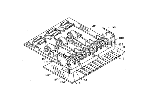
Re~erring now to FIG. 1, a two piece zero inaertion
-force connec-tor in accordance wi-th the pre~ent invention is
shown in per~pective form. As may be ~een in FIG. 1, a
mother board 11 t having a plurality of circuit conductors
such as 13 has a lower portion of the connector mounted
thereon. The lower portion of the connector con~ists of a u-
~haped plastic or other in~ulated material base unit 14,
having up~tanding earlike projection~ on either end thereof
de~ignated 15A and 15B located on each of the end
projection~ and projecting portions are pivot pins 16A and
16B, respectively. Included in the ba~e 14A are a plurality
of contacts like l9A which pass through the ba~e portion of
lower connector section 14 and make electrical contact with
the circuit connector cond~lctor~ ~uch a~ 13. Shown in an
upright or vertical po~ition prior to joining the upper and
lower connector ~ections i8 daughter board 12 on which i~
~ounted at either end thereof the other portion of the zero
insertion force connector in accordance with the pre~ent
invention eon~i~ting of cireuit board ~upport~ 17A and 17B
each including a plvot receiv:lng slot ~uch as 18A and 18n
re~pectively. Al~o included are a plurality of eircuit
eontact~ such a~ 19~ which are electrieally eonneeted to the
". ,
~2~7~S~
componen-ts mounted on daughter board 12. Initially the two
halves of the connector are mated with the daughter board 12
perpendicular to mother bQard 11. A~ may be seen from the
drawing of FIC7. 1, the embo~3es on contact~ 19A and l~B
directly engage with each other aa the daughter board i~
brought down with the pivot ~lots 18A and 18B engaging the
pivots 16A and 16~. Because of the design of the contact~,
thi~ initial engagement f-orce i9 zero. The contacts are
engaged and the pivots rest in the pivot slots, the daughter
board i~ rotated 90 degrees to the location shown in FIG. 2.
It is during thi~ rotation that the contact forces and
contact wiping action are generated. A further
understanding may also be had by to reference to FIG. 3A and
3B wherein again the daughter board 32 i~ ~hown in the
vertica]. position relative to the mother board 31, but with
the pivot slots in the pivot pin~ and then as seen in FIG.
3B with the daughter board rotated 90 degrees to e~tablish
the connections. As may be seen in FIGa. 3A and 3B, a
daughter board combined support and lock 36 as shown in FI~.
3A or 35 and 39 ~hown in FI~. 3B is included as a portion of
the lower part o-E the connector. ~9 can be readily seen in
FIG. 3B the daughter board 32 once in the parallel or
horizontal po~ition relatlve to mother board 31 is
~upported and locked ~nto po~ition by ~upport 39 and
2~ adjacent daughter board such as 36 would be supported and
engaged by ~upport 36, etc.
Because the angle oE rotation i9 not criticall
~ub~tantial freedo~ of design i9 afEorded by means of the
~7~i
present arrangement when working in the planar mode. A~ may
be readily seen if the support members such as 39 and 35
were made much taller, the connector~ such a~ 33 and 37
(FIG. 3B) could be placed clo~er together and the card might
be rotated something less than a full 90 degrees such a~,
for example, 4~ degree~. In thi~ case the projected area on
the mother board occupied by the re~ultant a~sembly would be
les~ than three quarters of the space occupied by a fully
rotated card. In another arrangement, component height off
the mother board could be increa~ed and the ~pace below the
card could be u~ed to mount other component~. Such an
arrangement is ~hown in FIG~. 4A and 4B whereby placing the
conneckor half on the underside of the card as may be ~een
in FI~. 4B, the profile of components could be then moùnted
on the mother board underneath the daughter board.
As may be seen in FI~. 3A, 3B, 4A and 4B, when an
array o~ printed wiring boards are mounted on a mother
board, the sprillg latch for one card may be part of the
molded pla~tic housing of an adjacent connector. Such an
arrangement clearly minimize~ the amount of additional
mounting hardware required.
Referring now to FIG. 5A, ~hown in per~pective form is
an embos~ed blade contact, which may be considered a
preferred de~:lgn for u~e Ln the connector of the present
invention. Both contact~ 61 and 52 are identical as used in
the two halves of the connector of the preseDt invention.
During zero force engagement, the raised ~ide 54 of the
g
, .
~zc~
embo~s o~ one contact is nested in the recessed side 53 of
the emboss on the other contact ~1. The top view of both
contncts prior to engagement is shown in FIG. 5D ta~en along
lines ~D and 5D' shown in FI~. ~B, wherein i-t can be readily
seen how contacts 51 and 52 have their raised and depressed
portions o-f the embosses nesting in each ~ther. Because o~
the design of the embosses, zero force engagement takes
place.
When the contacts are rotated 90 degree~ to each other
as shown in FIG. 5C, the embosses then interfere with each
other and the resulting interference causes the contacts to
be forced apart as can be seen in FIG. 5E, which is taken
along section lines 5E and 5E prime of FIG. 5C. It is this
force that generates the contact force to create a reliable
two point electrical contact. Both contacts may be plated
with a noble medal1 such as gold, which is typical practice
for electrical contacts of this nature.
In practice, these contacts would be arranged in their
connector bodies with every other contact of embo~s ~acing
one way, with the remaining con-tact~ facing in the oppo~ite
direction. By doLng thls, the contact ~orces generated
during gO degree rotation cancel each other out thereby
eliminating any ~ide thru~t eorce~ between mating connector
halve~. Plvot pLns and locking pLvot slot~ located at the
end~ of -the connectors act a~ the pivot points during
rotation and also prevent the connector halves from
di~enagiDg during and after rotation as may be seen again
by referring to FIGS. 1 and 2.
~Z97~5~;
Con-tact sequencing (make first, break last, e-tc.3 can
be accomplished by changing the relative ~izes o-f the two
embosses and selectively loading them in the connector body
during manufacture. When the recess side o~ the embo~s i~
wider than the raised emboss on the mating contact, the
point at which electrical contact is e~tablished, occurs at
a different angle during the rotation than when both
embo3se~ are the same size and width. Thus, by varying the
relative sizes of the embosses, such as 53 and 54, as seen
in FIG. 5A, it can be readily seen that normal make first
and make last contact types can be created and employed
within the same conhector body. It should also be noted
that since this contact system i8 hermaphroditic in nature,
it i9 pos~ible to double the useful lif~ (that i9 the Dumber
16 of mating and unmating cycles) if initially the-near sides
of the contacts are mated and then they are repositioned
withill the connector ~o as to engage the far sides. This
; duality of electrical contact surfaces could be used to
double the longevity of the connector ~ystem in accordance
with the pre~ent invention when utilized ln the field.
An additional Eeature o~ the present contact sy~tem i~
that rotation of the contact is not necessary to develop the
contact forces to create a reliable connection. Straight
translation along the axis of the emboss will also create
26 contact. If the length I,2 of the rece~ed emboss as seen in
FI~. 5A is much smaller than the length Ll of the raised
emboss, contact engagement will occur when the depth of
11
~29~95~
insertion is equal to ~2. I~ -~ull depth inser-tion iB equaL
to Ll, then the point of electrical contact will occur on a
line equal in len~th to Ll - ~2. By using thi~ embo~ blade
contact in both the rotatiDg and tran~l~ting mode3, it is
possible to double the number of input and output
connection~ on a given daughter board/mother board
combination. That i~, addi-tional connectors could be placed
on the end of daughter board~ at the end opposite to those
previou~ly described; with direct non-rotating contact being
e~tablished as outlined above.
FIG. 6A show~ in perspective a split blade contact
design wherein a groove pas~es through the center of the
embossed ~ection. Mating occurs as ~hown initially in FIGo
6B and 6D where the embo~ses nest within each other and then
upon rotation as ~hown in FIG. 6C contact is establi~hed a~
shown in FIG. 6E.
FIG. 7A show~ in per~pective another contact design,
utilizing embo~ed blade and fork arrangement, wherein the
embos~ed or projection ~ection placed within the fork and
Ealls within the fork as ~hown in FIG. 7B ~nd fall~ within
the opening of the Xork a~ ~hown in FIG~ 7D. Upon rotation,
the rai~ed or embos~ed portion forces the edge~ of the ~ork
to deflect and to prov:ide a firm contact a~ ~hown in FIG.
7E.
FI~. 8A 0how~ :in per~pective .Porm a rotat:ing wedge and
fork zero in~ertion force contact de~ign wherein the
rotatin wedge i~ in~erted within the fork and then on
rotation as ~hown in FIG. 8C e~tabli~he~ contact with the
12
fork edges as shown in FIG. 8E. Such an arrangement ha~ all
the attributes of the arrangement shQwn in FIG. 7, excep-t
that the method of' generating the contact forces between the
wedge and the fork is di~ferent. In the arrangement shown
in FIG. 8A, the wedge is shaped like an elipse where
dimension a, as may be seen in FIG. 8B, is larger than
dimension b. The width of the ~lot c is larger than b and
smaller than a. During engagement dimension b beiDg smaller
than dimension c, permits zero insertion f'orce operation.
When the two are rotated 90 degrees to each other, as can be
seen in FIG. 8C, the wedge is caused to spread the tines of
the f'ork due to the inter~erence created by dimension a o~
the wedge and dimension c of the fork. Two point~ of
contact having a f'orce e are created on the inside surface
of' the fork as shown in detail in FIG. 8C and also as may be
seen in the side view taken along the ~ection lines 8E and
8F, as shown in FIG. 8E.
FIG. 9A shows in perspective a levered wedge and fork
arrangement of zero force con-t~ct design. Rotation i~
required to actuate the contacts but the angle o~ rotation
is much le~ than 90 degree~, the pivot point no longer at
the point of` contact a~ it wa~ in the previou~ly de~cribed
de~ign0. In this ca~e, the weclge in the upper portion
appear~ as a cyl:inder having u diameter equal to dl. The
lower portion, or fork, has a slot width, as may be ~een in
FIG. 9~, equal to d2. Diumeter of` dl i~ greater than
diameter d2 by a pre~cribed amount. When the wedge and f'ork
13
~9~5i6
as~embly are engaged, a~ shown in FIG. 9C, and rotated
through an angle about the pivot point, as can be ~een :in
FIG. 9D, -the wedge i~ forced into the fork slot with an
iDterference fit. It is this interference fit that
generates the nece~sary contact force F against contact
point B.
A final contact arrangement is ~hown in perspective
form in FIG. lOA in which a narrow slot effectively i~
placed through the center of embos~ed blade contacts, as may
1.0 be seen in FIG. lOA and lOB. This so-called bifurcated
arrangement increa~e the probability of maintaining
electrical contact in an environment containing in~ulating
particulate matter. In this case~ bo-th of the mating
corJtacts are bifurcated, the re~ult i~ quadruplicated
electrical points of contact wherein normal bifurcated
contact3 re~ult in only two point0 of contact rather than
four. Very few contact ~ystem~ arrange for four points of
contact becau~e of the high co~t normally associated
therewith. In the pre~ent arrangement the embos~ed blade
~y~tem provides the nece~ary four points of electrical
contact at little or no extra co~t.
A~ noted above, while the unique rotating contact ~ero
in~ertion force connector of the present des:ign can employ
any of the contact arrangement~ aet forth above, that ~hown
FIGS. 5A, 5B1 6C i~ preferred.
While a number of embodiment3 of the pre~ent invention
are ~hown, it will be obviou~ to those ~killed in the art
that numcrou~ modifications can be made without departing
.
~97~315~
from the spirit of the present inventlon which ~hal]. be
limited oDly by the ~cope of the claims appended hereto.