Note: Descriptions are shown in the official language in which they were submitted.
~z~
REAL TIME DIGITAL SIGNAL PROCESSOR
IDLE INDICATOR
FIELD OF_T~E NVENTION
This invention relates to arrangements which
measure the loading of a digital signal processor.
BACKGROUND AND S~MMARY OF THE INVENTION
The need often arises to measure the available
processing capacity of a computer. Digital signal
processors (e.g., microproces60rs) have become
commonplace in virtually every type of electronic
equipment. Such processors can be used to perform a
variety of unctions. The flexibility provided by a
processor i8 often advantageously used to augment
the functions provided by a ~ystem, or to perform
those functions using complex algorithms.
As a simple illustration, suppose one is
designing a band pass fllter for speech signals in a
communications system. An analog bandpass filter
constructed using operational amplifier~, re~istors,
and capacitors is one design option that is ~uite
cost effective and provide~ suitable performance in
many applications. To increase flexibility and
perormance, however, one miyht choose digital
filtering techniques in~tead of analog techniques.
In digital filtering, the filter characteristics are
determined not by the values and configurations of
amplifiers, resistors and capacitors, but by the
program control steps performed by a digital signal
processor (e.g., a microprocessor or some other
device capable of processing digital signals~. The
filtering characteristics of a digital filter (e.g.,
fre~lency roll-off, "corner" frequencies, and the
like) may be changed simply by modifying the
programming executed by the processor -- adding
tremendous flexibility to the system.
There is typically a desire to take advantage
of the capabilities of the processor to the fullest
extent possible. The same processor used to perform
the filtering can also be used to perform other
related (and even unrelated) functions. For
example, it may be desirable to use the processor to
generate signalling tones for various applications,
to provide system status information (e.g., to
illuminate indicator~ or drive alphanumeric
displays), to receive and process user commands, or
the like. The processor can be used to perform far
more complex filtering and other functions than
Z5 could be performed cost effectively with analog
ci rcuitry .
Unfortunately, not all program code is as
efficient as it could be, and even efficient code
performing complex functions in real time can cause
excessive processing loading. Processors have
minimum "cycle times" (the time the processor
requires to execute a single program control
instruction). In the digital filtering example, the
9~3~
processor mus~ process incoming signals in real time
in addition to performing any "overhead" and other
tasks. Processor "loading" (typically measured in
percentage of maximum loading) depends upon the
S incoming data rate, the efficiency and complexity of
the program control software, and the speed of the
processor.
As a simple example, suppose the processor is
capable of executing an instruction every
microsecond (10 6 seconds) and the incoming signal
to be filtered is sampled once every millisecond
(10 3 seconds). Suppose further that the filtering
software performs an average of 500 instructions on
each incoming sample -- reg~liring a total time of
500 x 10 6 seconds = 0.5 milliseconds of processing
time for each sample. Processor loading would then
be approximately 50% (or perhaps slightly above 50%
due to additional overhead tasks the processor must
perform). If the incoming æignal sampling rate iB
ZO increased to one sample every 0.5 milliseconds, the
processor loading will increase to around 100%.
Excessive processor loading is potentially
extremely detrimental. In the filtering example,
excessive loading of the processor may cause data to
be lost and/or introduce inaccuracies in the
filtering process. If the processor is fully but
not excessively loaded by its real time processing
functions, it may have insufficient additiona~
capacity to perform other functions it is ~ upon
to perform. On the other hand, faster processors
are typically much more expensive (and may not even
be available in some applications), and in a cost
effective design it is generally desirable to use
components having capabilities on the same order a6
the demands placed upon them.
Unfortunately, it is not always possible to
accurately predict how much loading a given
processor will experience while performing given
real time functions. Typical complex algorithms
perform a variable number of instructions on input
data dependinq upon factors which may be difficult
or impossible to accurately take into account.
Computer simulations are helpful, but since they can
only simulate actual operating conditions they may
be inaccurate. It is therefore preferable to
actually measure processor loading under various
different operating conditions.
Diagnostic programs which run concurrently with
a processor's normal programming in order to measure
processor loading are generally known. This type of
diagnostic program may be called by an operating
system program (if one i5 provided), or
alternatively, may be interrupt driven and called
periodically (e.g., whenever a timer times out).
The diagnostic program may measure various
parameters of processor loading (e.g., count
processor cycles, and/or read the contents of
processor work areas such as status register, stack
contents, and the like) and, based on these (and
other) parameters, calculate an indication of
in~tantaneous or average loading. A history of such
indications may be stored and analyzed to provide a
measure of processor loading under various operating
conditions.
Unfortunately, such diagnostic programs are
generally complex and typically themselves add
significantly to processor loading -- causing the
indications they provide to be inaccurate in some
circumstances and adding to processor loading during
measurements. A program which determines processor
loading by counting processor cycles may
underestimate the loading of a very busy processor
because the processor may have insufficient
resources to increment the cycle counter. A further
shortcoming of such diagnostic programs is that they
attempt to estimate how much of the time a processor
is busY -- whereas in most cases a more relevant
inquiry is how much time the processor is not busy
(and is therefore available to perform additional
tasks).
It would be highly desirable to provide a cost
effective arrangement which measures average
processor loading and yet is non-invasive in that it
is completely transparent to the operation of the
processor (i.e., does not itself add to processor
loading). Such an arrangement would be even more
useful if it were capable of directly measuring the
amount of available processing capacity under a
variety of different operating conditions.
The present invention provides these and other
advantageous features by including diagnostic
instructions in the processor "idle loop."
A processor does not cease performing
instructions when it i~ not bu~y, but instead ~umps
or "traps" to a so-called "idle loop" whenever it is
idle. The idle loop generally consists of
instructions which perform no useful function (e.g.,
"no operation," delay and/or jurnp instructions).
When the processor must perform a function, it
,
rec~ives an "interrupt" -- at which time it ceases
performing instructions in the idle loop and begins
performing other, useful program control
instructions. The next time the processor has no
further tasks to perform, it once again returns to
it~ idle loop.
The present invention includes instructions in
the processor idle loop which control the processor
(or external circuitry associated with the
processor) to measure the amount (or percentage) of
time the processor operates in the idle loop. In
the preferred embodiment, instructions in the
processor .idle loop control the processor to
alternate a processor data output between output
states. The processor data output alternates
between states whenever the processor is idle, and
remains in the same state when the processor is
performing useful tasks. A fre~uency counter or
other indicating device (e.g., a light emitting
diode) responsive to the rate of processor data
output state change may be used to directly indicate
the amount of time the processor is idle relative to
the total amount of processing time.
Since the change of state, not the state
itself, of the data output is detected, it does not
matter what state the data output is left in when
the processor i8 interrupted from performing the
idle loop instructions (by design, the priority
associated with executing idle loop instructions is
lower than the priority associated with executing
any other instruction).
Because the processor performs the idle loop
instructions only when it has nothing else to do,
~3t7~
the additional idle loop instructions add nothing to
processor loading and the load detecting arrangement
accordingly is completely transparent to the
operation of the processor. Moreover, the idle loop
instructions directly measure the amount of time the
processor spends in an idle state relative to the
total amount of processing time -- and therefore
provide an extremely useful, direct indication of
spare processing capacity. These advantages are all
provided by an arrangement which adds only minimal
cost to the processor system.
These and other features and advantages of the
present invention may be better and more completely
appreciated by referrinq to the following detailed
description of presently preferred exemplary
embodiments in conjunction with the appended sheets
of drawings, of which:
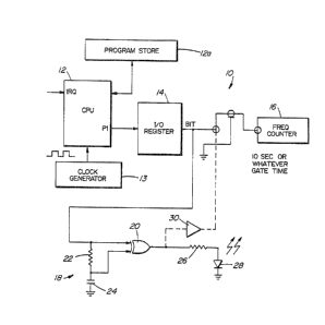
FIGURE 1 is a schematic block diagram of a
presently preferred exemplary embodiment of the
present invention;
FIGURE 2 is a schematic flowchart of exemplary
program control steps executed by the processor
shown in FIGURE l during idling; and
FIGURES 3A and 3B are exemplary load-indicating
output waveforms produced by the processor shown in
FIGURE l.
s
DETAILED DESCRIPTI~N ~F TEE DRAWINGS
FIGU~E 1 is a schematic block diagram o the
presently preferred exemplary embodiment of a
digital signal processing system 10 in accordance
with the present invention. System 10 includes a
central processing unit ("CPU") or processor 12.
Processor 12 may, for example, be a conventional
microprocessor including a read only memory proqram
store 12a, internal registers and an arithmetic
logic unit, etc. -- or virtually any other type of
device which processes digital signals. A
conventional clock sign~l generator 13 produces a
periodically-alternating digital clock
synchronization signal which drives processor 12.
The frequency (that is -- the period) of this clock
~ignal determines the time it takes for the
proce~sor 12 to execute each of its program control
instructions.
In the preferred embodiment, processor 12 may
be connected to a variety of associated conventional
external circuits which perform various desired
functions. For example, if processor 12 is to be
used to provide digital filtering, it may be
connected to the output of an analog-to-digital
converter or other source of digitized signals (not
shown). Processor 12 may also be connected to
display devices, input/output peripheral devices, or
virtually any of the thou~ands of different devices
designed to be interfaced with a processor (all as
is well known to those skilled in this art).
In the preferred embodiment, processor 12
includes at least one unused data output connection
g
Pl which is connected to the input of a conventional
input/output (I/O) register 14. I/o register 14 is
sensitive to the "edges" ~transitions) of the Pl
output of processor 12 and produces an output signal
"BIT" which changes state in response to those
edges. In the preferred embodiment, register 14
buffers the signal outputted at the processor P1
data output, but does not alter the frequency of
that signal (and may but need not necessarily
synchronize the signal to the processor clock).
The register 14 "BIT" output is connected to
the input of a freguency counter 16 operating as an
event counter with a fixed gate time (of, e.g., 10
seconds). The "BIT" signal output of register 14 is
also connected to a visual indicating circuit 18
(which can conveniently be provided on the same
board as processor 12) providing a rough visual
indication of processor idle percentage.
Indicating circuit 18 in the preferred
embodiment includes an exclusive OR ("XOR") gate 20
the inputs of which are connected across a resistor
22. The "BIT" signal is connected to a first input
of XOR yate 20, and a second input of the XOR gate
is connected through a capacitor 24 to ground
potential. This input configuration of XOR gate 20
causes the XOR gate to produce a pulse whenever a
transition occurs in the "BIT" output signal (since
the XOR gate first input immediately changes levels
to track a level change of the "BIT" signal, but the
gate 6econd input changes ~tate only after a delay
determined by the RC time constant of resistor 22
and capacitor 24).
The output ~f XOR gate 20 is connected through
~2~7~
a current limiting series resistor 26 to the anode
of a light emitting diode (LED) 28 -- the LED
cathode being connected to ground potential. An
optional driver/buffer amplifier 30 may be used to
connect the output of XOR gate 20 to the frequency
counter 16 input in lieu of a direct connection
between the counter input and the register 14 "BIT"
signal output.
As will be ur.derstood by those skilled in the
art, it is not necessary to provide both frequency
counter 16 and indicating circuit 18 in the
preferred embodiment, since both are used to
indicate the same information. In the preferred
embodiment, freguency counter 16 is only connected
when an exact load measurement is desired, while
indicating circuit 18 is continuously connected to
I/O register 14 so as to provide a constant visual
indication of processor idle percentage.
FIGURE 2 is a schematic flowchart of exemplary
program control steps performed by processor 12
whenever the processor is in an idle state. In the
preferred embodiment, processor 12 executes a
section of code beginning at a predetermined address
(of its associated read only memory program store
12a) whenever it i8 at idle and is not reguired to
perform useful tasks. Program control instructions
specifying the tasks shown in the FIGURE 2 flowchart
are loaded into the proyram store 12a beginning at
that predetermined address and are therefore
executed whenever processor 12 is at idle.
Processor 12 is "interrupt driven" in the
preferred embodiment, meaning that it begins
executing program control instructions stored in a
portion of program ~tore l~a other than that portion
storing the instructions executed during idle in
response to the occurrance of an external event
(e.g., receipt of input data to be processed).
Typically, a device external to processor 12 (2.g.,
a conventional I/0 controller not shown) produces a
signal which is applied to a processor interrupt
request (IRQ) input. The presence of an active
6ignal level on this interrupt request input causes
the microprocessor to cease executing the "idle"
routine and to "trap" to an interrupt handler
routine 6tored in a different portion of program
store 12a. The interrupt handler routine either
itself performs desired processing (e.g., to process
the input data which caused an I/0 interrupt to be
generated) or alternatively, transfers program
control to additional routines (also s~ored in
program store 12a) which perform the desired
processing. When processing i8 completed, processor
12 once again returns to executing the idle routine.
The FIGURE 2 idle routine is very short in the
preferred embodiment. A first step 50 writes a
logic level one to processor data output connection
Pl. A second step 52 writes a logic level zero to
the processor data output connection P1. The
routine then jumps bac~ to the ~irst step 50 to
repeat steps 50, 52.
The following are exemplary mnemonic
instructionR for performing the steps shown in the
~ 7~
12
FIGURE 2 flowchart:
ADDRESS INSTRUCTION
X Set Pl
X~1 Reset Pl
X+2 Jump to Address X
The steps ~hown in the FIGUR~ 2 routine form an
endless loop that causes process~r data output Pl to
"toggle" (that is -- alternate between binary values
O and 1) at a rate proportional to the processor
clock rate whenever the processor 1~ is idling, and
causes data output Pl to remain constant when the
processor is performing useful tasks. For example,
as6ume processor 12 has a one megahertz clock
frequency, executes the "set" and "reset" commands
each in one cycle time (one microsecond), and
executes the "jump" command in two cycle times (two
microseconds)~ The total time required to execute
the "idle loop" consi~ting of these three
instructions one time i8 four microseconds, and a
single loop execution will cause data output Pl to
alternate once between logic level O and logic level
1 (e.g., from O to 1 to 0, or from 1 to O to 1) --
resulting in a signal of one-~uarter the processor
clock fre~uency being generated whenever (and only
when) the processor has nothing to do and i8 idling.
The signal present on the processor P1 output
does not have a 50% duty cycle in the preferred
embodiment even when processor 12 is 100% idling and
the idle endless loop steps shown in FIGU~E 2 are
performed continwously. This is because the Pl
13
output state remains constant during the time
processor 12 executes the "jump" instruction. In
the preferred embodiment, the P1 output rises ko
logic level 1 only while processor 12 execute~ the
"reset" instruction (that is, during the processor
cycle immediately after the "set" instruction has
been performed). The Pl output then falls to logic
level 0 immediately after the "reset" instruction
executes -- and remains at logic level 0 during the
time the "jump" instruction is executed as well as
during the time the "set" instruction is performed.
It is for this reason that freguency counter 16 (and
indicating circuit 18) is sensitive to transitions
in the "BIT" signal rather than to some other
characteristic of that signal.
Freguency counter 16 in the preferred
embodiment directly indicates the percentage of time
processor 12 is idle relative to the total
processing time by counting edges of the signal
"BIT" produced by I/0 register 14. If the processor
is 100% idle, then edges (e.g., leading edges) will
occur at the rate of l/T where T is the time
required ~y processor 12 to execute the idle loop
instructions once (e.g., 4 microseconds in the
example given above -- which eguals the time
required to perform a ~et bit instruction + the time
required to perform a reset bit instruction + the
time required to perform a jump instruction in the
preferred embodiment). As the processor 12 does
more and more real work, it spends less time
executing the idle loop instructions -- and the
edges occur proportionately less often in direct
ratio to the amount of idle time which remains.
14
Assume, or example, that fre~lency counter 16
receives one pulse (edge) every 4 microseconds when
processor 12 is 100% idle (as described in the
example above). Suppose frequency counter 16 has a
gate time of 10 seconds (selected to provide a
desired degree of averaging over time). With
processor 12 100% idle, frequency counter 16 will
count 2.5 x 10⁶ pulses (edges) over the ten second
gate time (onP pulse every 4 microseconds means
250,000 pulses every second, or 2.5 million pulses
every ten seconds). Note that it is helpful for
this calculation to know (at least approximately)
the relationship between the processor clock
frequency and the gate time, as well as the number
of clock cycles required to execute the idle loop in
its entirety. A waveform of the l'BIT" signal for
100% idling of processor 12 is shown in FIGURE 3A.
Suppose frequency counter 16 counts 1.25 x 10⁶
pulses (edges) during its ten second gate time.
This count indicates that over the ten second gate
time, processor 12 was 50% idle on the average. As
i6 shown in FIGURE 3B, this 50% idling condition
does not halve the instantaneous frequency of the
"BIT" signal. Rather, the "BIT" signal is generated
at substantially the same frequency whenever
processor 12 is idling in the preferred embodiment.
However, processor 12 ceases to produce the "BIT"
signal altogether during times when it i8 performing
real work (i.e., useful tasks) rather than idling.
When the frequency of the "BIT" signal is averaged
(integrated) over a time period which is long
relative to the time between processor clock pulses,
the result is a highly accurate indication of
7~P8~
average processor idle percentag2.
The indication provided by LED 2~ will
obviously not provide as accurate an estimate of
processor idle time as that provided by frequency
counter 16. However, the LED 28 does provide an
indicator which is also very helpul. If LED 28 i~
fully lit, processor 12 is nearly 100% idle (the LED
will actually have an on-off duty cycle of about 50%
under this condition, but the alternations are ~o
rapid as to be undetectable by the human eye). If
LED 28 is dark or nearly dark, processor 12 is 0%
idle. If LED 28 is at half brightness compared to
the 100% condition, processor 12 is operating at 50%
idle.
In some applications it might be desirable to
substitute a conventional frequency ratio detector
for frequency counter 16. Such a detector may
compare the ratio of the processor clock frequency
to the frequency of the "BIT" ~ignal to provide an
indication of the percentage of processor time spent
idling.
While the invention has been described in
connéction with what i8 presently considered to be
the mo6t practical and preferred emhodiments, it is
to be understood that the invention is not to be
limited to the di~closed embodiments, but on the
contrary, is intended to cover various modifications
and equivalent arrangements included within the
spirit and scope of the appended claims.