Note: Descriptions are shown in the official language in which they were submitted.
026gP
237~0
OPTICAL DEVIC
~ he lnventlon relates to an optlcal dev~ce for use
for example as an opt~cal ampl~f~er or log~c element.
A paper ent~tled "Nonl~near antlresonant r~ng
~nterferometer" ~n Optics ~etters, Yol,8, No,9, pages
471-473, by Ken~u Otsuka~ descr~bes an ~nterferometer
compr~s~ng a beam splltter to spl~t an opt~cal beam lnto
portlons o~ d~fferenS ~ntensit~es, a palr of m~rrvrs on to
respect~ve ones of wh~ch the port~ons ~mpinge, and a ~lock
of non-linear mater~al posit~oned ~n ~he opt~cal path
between ~he mlrrors, L~ght ls spl~t at ~he beam spll~ter
lnto the dlfferent lntensi~y port~ons which are then
caused to pass ~n oppos~te d~rect~ons through the
non-l~near med~um wh~ch has the affect of ~mpart~ng
dlfferent phase shlfts on the l~ght portions due to lts
non-l~near refractlve ~ndex property. The phase sh~fted
port~ons are recomb~ned at the beam spl~tter.
~ he Otsuka deY~ce relles on cross-~nteractlon
~etween the two counter propagat~ng optlcal flelds and ls
dependent on ~nterference between the f~elds produclng a
non-l~near ~ndex grat~ng w~th~n the non-l~near med~um. In
these clrcumstances the counter propagatlng flelds ln the
devlce are ne~essarily of a durat~on which exceeds the
propagation per~od w~thin the non-l~near med~um. The
dev~ce operat~on requlres the opt~cal f~elds to be
co~nc~dent ~n the non-linear med~um thereby necessitat~ng
preclse locat~on of the non-l~near me~um at the mid-po~nt
of the op~lcal path around the dev~ce. One of the
proble~s w~th this dev1ce ls therefore the need for
accurate pos~t10n~ng of the var~ous components. For
example, the mlrrors also have to b~ Yery arcurately
al~gned w~th the non-l~near medlum and wlth each other.
~'
~298~ ~
In addition, to avoid problems which would arise from field
divergence within an extended non-guiding medium, the
length of the non-linear medium is itself restricted.
There is a further risk of diffraction problems because the
optical fields are laterally unconstrained during
propagation around the device i.e. the ~ields could spread
out laterally which would reduce their intensities.
It is an object of the present invention to
provide an optical device which substantially overcomes or
at least mitigates the aforementioned problems and
restrictions. It is a further object of the present
invention to provide a method of operation of such a
device.
In a first aspect the present invention provides
an optical device comprising a coupling means having first
and second pairs o~ optical communication ports, in which
portions of an optical signal received at a port of one
pair are coupled into each port of the other pair in a
predetermined coupling ratio; and an optical waveguide
including a first material having a non-linear refractive
index, and a second material in series with the first
material, the first and second materials having non-
commuting effects on an optical signal at a working
intensity travelling alony the waveguide, the optical
waveguide coupling together the first pair of ports; the
coupling ratio and appropriate waveguide parameters being
selected such that in use the portions of an uptical signal
at a working intensity received at one of the second pair
of ports of the coupling means, and coupled into each end
of the waveguide, return to said coupling means with an
intensity dependent relative phase shift after travelling
around the waveguide.
In contrast to the known device described above,
the present invention makes use of an optical waveguide
including a material having a non-linear refractive index.
This not only enable previously encountered alignment and
1.:~,;
.. ....
298~2
diffraction problems to be avoided, but furthermore
provides more flexibility in operation and avoids the
constructional limitations of the earlier device. Further,
the present device does not require cross-interaction
betwe0n counter propagating fields, nor the establishment
of an interference grating. Thus, in contrast to the
device of Otsuka, the present device snables an intensity
depend~nt relative phase shift to be achieved where the
duration of an input siynal is shorter than the signal
transit time through the non-linear medium or material.
The non-linear material may also be conveniently
distributed throughout the waveguide.
In the present device the appropriate waveguide
parameters, the coupling ratio, or a combination of both
may be selected to break the device symmetry and so obtain
a relative phase shift in the counter propagating portions
as will be further described below. Thus, for example, the
coupling ratio may be symmetric (50:50~, in contrast to the
Otsuka device where it is essential for the beamsplitter to
be asymmetric (i.e. other than 50:50) as the optical path
in this device is otherwise symmetric.
The waveguide parameters which may be
appropriately selected to affect the device symmetry
include, for example, the waveguide length, the non-linear
refractive inde.x n2 (Kerr co-efficient~, the dispersion k2,
the mode field width, and the like. These parameters may
be allowed to vary along the length of the waveguide.
In this specification by "non-linear" we mean that
the r~fractive index of the material varies with the
intensity of the transmitted signal. Typically, the
refractive index n is given by the formula:-
n=nO+n2 ¦E ¦2
where nO is the linear refractive index, n2 is the Kerr ro-
efficient, and 1E¦ 2 is the intensity of the transmitted
signal.
1 ,
9~ 2
In one preferred arrangement, the coupling means
has a coupling ratio of other than 50:50 (i.e. the
intensities of signal portions coupled into the ends of the
waveguide
~ .~,
o~i
~, ~ .
1 29 !3~1Z
- 4 -
are not equal) In thls s~uat~on, s~gnals wlth d~fferent
lntens~t~es are fed ~n oppos~te d1rect~ons around the
wavegu~de thus resultlng ~n the s~gnals exper~enc~ng
dlfferent refract~ve ~nd~ces. As w~11 be expla~ned below,
thls resul~s In the s~gnals experlenclng d~fferent phase
sh~fts so that when the s~gnals return back to the
coupl~ng means, they have an ln~enslty d~pendent relat~ve
phase shlft. By varylng the coupl~ng r~t~o and/or ~he
length of the wavegu~de, for example, It ~s possible to
vary the ph~se sh1ft between the re~urn~ng s~gnals ~or any
par$1cular workin~ intensity of input slgnal.
The ~ntensity dependence of the relatlve phase sh~ft
rPsults ln a dev~ce whose output ~s an osclll~tory
funct~on of the ~ntens~ty of the ~nput s~gnal. Thls
property can be used ln a var~ety of appllcatlons
~nclud~ng log~c elements, optlcal ampl~f~ers, optlcal
sw~tches and the l~ke.
In another arrangemen~g the wavegu~de may further
compr~se a second mater~al ~n ser~es with the flrst
mater~al, the f~rst and second mater~als hav~ng
non-commut~ng effects on an opt~cal s~gnal at a worklng
~ntenslty travell~ng along the ~avegu1de. In this
s~tuat~on, khe coupl1ng rat~o of the coupl~ng m~ans could
be 50:50 s~nce the non-commutlng mater~als can be arranged
to automat~cally produce the requ~red rel~t~ve phase shlft
even ~n s~gnal port~ons w~th the same ~nput ~ntens~ty.
The second mater~al ~s preferably a dlspers~ve mater1al.
Conventionally, ~t ~s desirable to m~n~m~se dispersion
effects, both by fabricat~ng wavegu~des w~th low absolute
d~spers~on and by opera~ing at wavelengths around the
d~spers~on ~ero for the wavegu~de. However, a waveguide
accordlng to the present ~nvent~on can be fabr~cated wlth
different dlsperslve propert~es at d~fFerent port~ons.
For example, differences ~n total d~spers~on can be
ach~eYed by varyIng the waveguide refract~Ye ~ndex
prof l l e, Accordl rg to th~ l ength of he wavegu1 de port1 on
~2~ 12
compr~slng the second mater~al, the d1sperslon must be
adequa~e, ln comblnat~on w~th an approprlate non-commuting
property, to proY~de the asymmetry requ~red to ach1eve th~
intens~gy dependent phase sh7ft. Su1table comb1nat~ons of
non-commut1ng propert~es ~nclude, for example9 d~spers10n
and elther (or both) of non-l~near~ty n~ and mode f~eld
w~dth. Alternat7vely, for example, the secnnd mat~r~al
may have non-l~near polar1sat~on rotat~on propertles whlch
do not commute w~th those ment~oned a~ve. Appropr1at~
alternat~ve comblnat~ons o~ these and ~ther propert~es
will be appar~nt to those sk111ed ~n the art.
It should be noted that where the waveguide
compr~ses two or more ser1ally connected port~ons wlth
non-commuting properties then the order ~n wh~ch
non-~nteractlng, counter prcpagat~ng s19nals pass through
the portions becomes lmportant and chang~ng the order w~ll
generall~ result ~n a d~fferent ph~se change 7n th~
resultant s19nals arr1v1ng back at the coupllng means.
Dev1ces accord1ng to th~ ~nvent~on are operable to
produce an ~ntens~ty dependent phase sh~ft both when the
durat~on of the counter propagat1ng s~gnals exceeds the
trans7t tlme through the wavegu~de ~when cross-~nteract10n
dom~nates) and when the s~gnal durat10n 1s less than ~h~s
translt t~me (when the cross-~n~eractlon ls not
s~yn1f~cant). HoweYer, the operat~on of the deY~ce as
d~scussed above assumes that the ~nput s19nals are of
substantlally constant 1ntens~ty over the t~me taken to
propagate around the wavegu~de. ~or pulse slgnals thls
am~unts ~o an assumpt10n that the pulses are substant~a7)y
square. As pulse durat~on dec~eases, however, thls
assumpt~on ~s no longer val1d for real pulses w1th fln~te
r~se and fall ~lmes wh~ch compr1se a slgn~f~cant
proport~on ~f the overall pulse w7dth. In these
c1rcumstances each pulse envelope wlll conta~n a number of
cycles wlth a range of
I
. .
" ~98112
ln~ensi~les. In sillca9 for example, s~nce the non-l~near
refractive ~ndex responds ~o the ~nstantaneous intensity,
each cycle w~ll exper~ence a slightly different refractive
~ndex as ~t passes through the non-l~near materlal which
w~ll generally result in a variation ln phase sh~ft
betw~en cycles ~n the same pulse wh~ch may degrade the
bas~c device performance.
In a preferred embodlmeng of the present inYent~on,
to overcome or at least mltl~ate the potent~al problem
wh~ch may be presented under these condi~ions, the
wavegu~de compr~ses material whlch supports so1iton
e~fec~s when opt~cal pulses at appropr~ate work~ng
~ntens)t~es are in~ected ~nto the devlce, ~he length of
the wavegu~de mus~ then be sufflc~ent such that the
~ntens~ty dependent phase of an ln~ected pulse becomes
substantlally uniform throughout the pulse.
In th~s latter embod~ment the propert~es of the
wavegulde are selected such that the Kerr coe~f~cient,
n2~ and the group velocity dlsperslon have opposite
s~gns. Then, 1f the ~nput ~s of sufficientty hi3h
intens~ty, the waveguide w~ll support pulses wh~ch
propagate substant~ally non-dlspersively over several
tlmes the length o~er which a low ~ntensity pulse would
d~sperse. Such pulses are ref~rred to as sol~tons. An
art)cle by N J Doran and K J Blow en~itled "Sol~tons in
Optical Com~unications", IEEE Journal of Quantum
EleGtronlcs, Yol.QE19, No.12, Dec.1983 prov1des an
approprlate discuss~on of sol~ton propagat~on. In the
present specif~cation a~d releYant cla~ms ~501)ton" ~S
taken to refer to any pulse which exh~b~ts ~he aboYe
property of substant1ally non-dlspers~ve propagat~on and
not only to so-called "exact" or "pure" solitons, for
example9 as hereinafter descr~bed.
Thls preferred embodlmen~, therefore, specif~cally
employ~ a waveguide w~th significant dispersîon of the
.
` 12~8~2
requ~red forln wh~ch perm~ts sol~ton propagat~on,
For sot~ton pulses the overall phase changes are
dependent on the 1ntens~ty of the pulse envelope as a
whole and not merely on the lnstantaneous lntens~t~es of
different port~ons of the wave traln as ~s the case with
non-sot~ton pulses. For the ~ntens1ty-dependent phase o~
a sol~ton pulse to be substantially un~form throughsut the
pulse, 1t has been found that sol~ons should propagate
over a wavegu~de length at least approx~mately equ~valent
to a sol~ton perlod or more as descr~bed below.
As w~th th~ preY~ous embod~ments of the ~nvention~
to ach~eve a non-zero9 ~ntensl~y-dependent relat~v~ phase
sh~ft between the wave tralns w~thln the counter
propagat~ng putse envelopes ~t ls necessary to break the
symmetry of the device ~n some appropr~ate manner.
Conven~ently, th~s may be done by us~ng an asymmetr~c
coupllng means (not 50:50) or by hav~ng wavegu~de port~ons
w~th dlfferent d~spers~ons or non-l~near coefficlents
n2, for example. However, s~nce the refract~ve ~ndex
var~es wlth n2xlntens~ty, an effect~ve asy~netry may
also be obta~ned by allowlng the ~ntens~ty ~n different
port~ons of the wavegu~de to d~f~er, Th~s may be
ach~eved, for example, by hav~ng d~fferent port~ons of the
waveguide with d~fer~ng mode f~eld w~dths. Any
comb~nat~ons of these d~fferences may also be used to
ach~eve a des~red asynMletry,
For sol~ton propagatlon, the wavegu~de prePerably
comprlses Inater~al wh~ch s~multaneously exhib~ts both the
dlspers~ve and non-linear propert~es as re~uired for
sol~ton propagat~on, Whilst ~t is poss~ble to ach~eve
sol~on propagatlsn under alternat~ve oond~ions, for
example, when the wavegu~de co~prises an a1~erna~ng
sequence of d~sperslve ~nd n~n-l~near eomponents, ~h~s ~s
not part~cular~y des~rable for sol~ton propa~at~on s~nce,
~L2~13112
as noted above, in physical terms, the effects do not
commute. Consequently, a large number of very short
lengths of waveguide with the alternating properties would
probably be required to achieve a reasonable approximation
to the conditions for effective soliton propagation.
Preferably, the waveguide i5 a single mode
waveguid~. Conveniently, the optical waveguide is formed
from optical fibre, preEerably monomode optical fibre.
Alternatively, for example, the waveguide may be fabricated
in planar (e.g. lithium niobate) waveguide form.
Non-linear properties may be provided by
appropriately doping the waveguideO It is also possible,
for example, to introduce non-linear behaviour by providing
suitable non-linear material as an overlay on a
conventional waveguide. For instance, an optical fibre may
have some cladding etched away sufficiently to allow
coupling of its optical field into an external overlay of
non-linear material without necessarily exposing or doping
the fibre core. Similarly the dispersive properties may be
provided by doping or other techniques. For example, a
dispersive grating may be provided in the waveguide.
Also preferably the waveguide includes inherent
polarisation control or is positioned in series with a
polarisation controller. Where the waveguide exhibits
birefringence, or example, polarisation control enables
the input to be appropriately adjusted or maintained to
provide consistent and predictable device performance.
According to another aspect of the present
invention a method of processing an optical signal
comprises the steps of: providing an optical device having
a coupling means having first and second pairs of optical
communication ports, in which portions of an optical signal
received at a port of one pair are coupled into each port
of the other pair in a predetermined coupling ratio; and an
optical waveguide at least a portion of which includes a
first material having a nun-linear refractive index, and a
-,
. . .,:3
~2~ LZ
second material in series with said first material, the
first and second materials having non-commuting effects on
an optical signal at a working intensity travelling along
the waveguide the optical waveguide coupling together the
first pair of ports; the coupling ratio and appropriate
waveguide parameters being selected such that in use the
portions of an optical signal at a working intensity
received at one of the second pair of ports of the coupling
means, and coupled into each end of the waveguide, return
to said coupling means with an intensity dependent relative
phase shift after travelling around the waveguide; and
inputting an optical signal into one of th~ second pair of
ports of khe device to produce tWQ counter propagating
signals within the waveguide, thereby to provide a
processed pulse signal output at least at one of the second
pair of ports.
Preferably, the method comprises inputting an
optical signal having a duration less than the transit time
for propagation arouncl the waveguide and of substantially
constant input intensity.
The processing may be to per~orm logic functions
on, to amplify, switch or otherwise modify an input signal.
The processed signal output will correspondingly comprise
a logical output, an amplified, switched or otherwise
modified signal. Criteria and preferences for the
selection of device parameters are as described above with
reference to the invention in its first aspect.
Alternatively, or additionally, for processing an
optical signal comprising pulses capable of soliton
propagation the method comprises the steps of: providing
a device according to the invention in its first aspect
including a waveguide whose parameters are selected for
soliton propagation; inputting a pulse signal into one of
the second pair of ports of the device, at an amplitude
appropriate for soliton propagation in the waveguide,
thereby to produce two counter propagating signals within
l.,,
. ,~.
- 1298~Z
9a
the waveguide and to provide a processed pulse signal
output at least at one of the second pair of ports.
The device parameters are selected appropriately
to influence the soliton propagation according to the
processing required.
Embodiments of an optical device and methods of
operation according to the invention will now be described
by way of example and with reference to the accompanying
drawings~ in which:-
Figure 1 is a schematic diagram of a device;
B
L2~
10 -
F~gure 2 ~llustrates graph~cally the varlation
between ~nput lntens~ty and output ~ntenslty (af~er
normallsatlon) for ~wo d~ff~rent coupl~ng ratios;
F~gure 3 ~s a graph ~llustratlng the propagatlon
character~stlcs of a de~J~ce according ~o the
~nvention for a pulse ~nput;
F~gure 4 ~llustrates a ser~es of devices coupled
together; and
F~gures 5 and 6 show dev~ces accordlng to the
~nven~on In fur~her conf~guratlons.
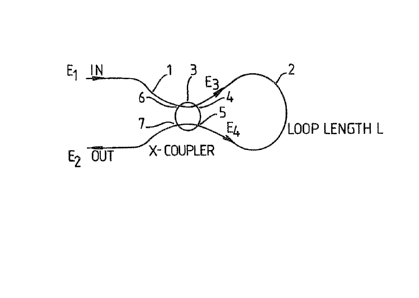
The optlcal dev~ce shown ~n Flgure 1 is deflned by a
single sillca opt~cal fibre 1 formed lnto a loop 2.
Port~ons of the optlcal fibre ltself are pos~t~oned close
to one another to deflne an X coupler 3 hav~ng a p3ir of
f~rst ports 4, 5 and a palr of second ports 6, 7. The X
coupler 3 ~s adap~ed to couple portions of an optical
s~gnal rece~ved at the ports 5 or 7 into each of the ports
4~ 5 ln accordance wlth a predeterm~ned coupl~ng rat~o.
S~m~larly, optlcal signals arr~v~ng at the coupler 3
recelYed by e~ther the port 4 or port 5 w~ll be coupled by
the same coupl~ng rat~o lntc the ports ~, 7.
Thus, under normal (l~near) c~rcumstances ~he device
shown ~n F~gure 1 w~ll operate as a m~rror. That ~s wlth
the input E1 at the port 6; the l~ght all returns back
to the port 6 ~f the coupllng ratio ls 50:50. Any other
alue for the coupllng ratlo gi~es an appropr~ate spllt ~n
the output power between the two ports 6, 7.
The coupl~r 3 causes a s~ngle lnput ~o be split ~nto
two counter propagatlng fields whlch return in co~nc~dence
I to comb~ne back at the coupler. The opt~cal pa~h leng~h
i ls prec~sely the same for both propagat~ng fle~ds since
they follow the same path but ln opposlte dlrect10ns.
Thls ~s an lmportant feature of the dev1ce. Linearly the
flelds wlll emerge the same ~ndependent of wh~ch way round
.
`` ~2~3~LZ
- 11
they traverse the loop; non-llnearly th~s may not be th~
case. Below, a sltuation ~s descr~bed ln whlch
nsn-linearl~y breaks the ldent~cal propagatlon effec~s for
the t~o paths. The device descrlbed responds to
d~fferences ln phases of comb~nlng ~lelds and could
therefore be descrlbed as an Interferometrlc device but
there ~s no need for lnterferometr~c al~gnment of th~
opt~cal paths. Thls 1s an outstandlng feature of the
devlce.
The loop 2 of the wavegu1de ~s ~ormed a~ least
partly from ~ non-linear mater~al exhibltlng a refractive
~ndex n whlch var1es ~n accordance wlth the formula g~ven
above, The dev~ce operates ~n the 'small' non-linearlty
reg~me which means that ~t is only the phase that ls
altered and there are, for example, no effects on the
group veloclty. In the sm~ll non-l~nearlty regime, nO
ls much greater than n2¦E~2 (eg may be by a factor of
about lO6). The s~plest realisatlon of a non-l~near
dev~Ge based on the conf~guratlon of Flgure 1 ~s to allow
self-phase-modulation (SPM) ln the flbre loop wlth a
coupler 3 w~th coupl~ng rat~o ~ a)
SP~ glves a d~stance and ~ntens~ty dependent phase
sh~ft g~ven by
~ E) a (21n2¦E¦2L)/~ rad
where n2 ls the nonl~near Kerr coefficlent.
The coupler equat~ons for an 'X' coupler as ~n
F~gure 1 are:
E3 = aO'~El + ~51-a)O-5E2 (1)
E4 ~ a)0-5El ~ a~SE2 (2)
w~th the coupl~ng coefflc~en~ (eg for a 50:50 coupler
0.5, for a 60:40 coupler -0.4~.
We take the case of d s~ngle ~nput at port 6,
EIN. ~herefore: 5
E4 l(l-a) ElN
~2 9 8~1 2
12
Thus after travelling the d~stance L
E3- ~ INeXP~[a2~n21EINl L/)~]
F.4 ~ ) 0 ' 5EINexpi ~ ) 27rn2 l E IN~ 21/1]
For the return trans~t through the coupler 3 we need
the transform of equat;on 1, ie:
El , ~'5~3 ~ )0-~E~
E2 = -~(1-a)0'5E3 + aO-54
To calculate the output at 6 and 7 we need to
subst~tute 4=E3* and E3=E4* and obta~n:
a ~ a)-5EIN~exp-~ a)~(E~[N)3~exp-~(a~ N))~
E2-EINLaexp-~(~d(E1~3)-~1-a)exp-~ 3~(EIN))i
The outpuS ~ntens~t~es are given by:
¦E1¦ ¦EIN¦ 2~(1-~t1~COS(I1-2~)d(EIN))]
I E2¦ 2= jEIN~ 2~1-a) ( 1~COS( ( 1-2a~ N ) ) ) ) ]
These equat~ons show that for any Yalue o,^ a,
100/o of the power emerges from por~ 7 when:
~ (E) ~ ~1-2~m
and the m~n~mum output power from port 7 is when:
~ E~ = 2~ 2a)m ,where m is an ~nteger;
1n wh~ch case:
¦E21 = 1-4~( l a)
wh~ch is the output for l~near fields.
The gener~l behaviour tor response characteristic)
~s shown ~n Figure 2, The output sw~tches from the low
power value to 100/o every time the pow0r ~ncreases by
~IEI 2 x ~
The best sw~tching rat~o occurs for a close to 0.5 but the
switching energy increases correspondinglyD In the lim~t,
for a 50:5~ coupler (a=0,5) the required f~eld would be
~nf~n~te.
For one sh~ft frQm m~nlmum to maximum output we
require:
¦E¦2L = ~ x
tl-~a~ n2
~.
,
., ~,
~298~L2
3 -
For sll~ca based ~1bres n2 - 3.2x10 16 cm2/Wm,
and tak~ng ~ = 1.06~m and f~bre area 100 ~m2 then:
l~l2L ~ X 5 x 10²
`I~I-Za~
For ~he example of ~ 0.4 then we need E 2 ~ 8kw
for L lm. If a = 0,1 then th~ requlred peak power comes
down ~o 1.~ kw but the sw~tchlng contras~ ls
correspond~ngly reduced as shown in Flgure 2.
The above calculat~ons are effectlvely for constant
~ntens~ty operatlon and do not treat the case where
d~sperslon ls slgn~f~cant. A slngle value has been taken
for the input ~ntens~ty ~n order to derive the output
resul~s, In real~ty, unless the Input can be cons1dered
as square pulses, the transm~sslon characteristic w~ll be
degraded by the vary~ng s~gnal ~ntenslty. S1nce the basic
dev~ce response 1s ~ust to the instantaneous ~ntenslty,
the basic de~ce would not work ~s e~fic~ently on shor~er
pulses where the variat~on ~n ~ntensity throughout ~he
pulse duratlon becomes signlf1cant.
It ls ~hen des~rable to mod1fy the de~ice to prov~de
s~gn~f1cant dlspersion as well ~s SPM ~n the waveguide and
lntroduce soliton propagat~on effects.
Solitons are generated by the comb1ned act1On of
self-phase modulat~on and dlsperslon in the negat~ve group
velnc~ty d~sperslon regime ~n an opt1cal waveguide. The
use of sol~tons In a non-l~near optlcal devlce is also
d~scussed ~n copend~ng patent appl~oatlon GB 8625~81 filed
22.10.86 in the name o~ the present appl~cants.
An exact slngle soliton does not change shape ~n Its
propagat~on through an opt~cal wavegu1de, but 1t does
acqu~re a phase sh~t proport~onal to ~he d~stance
~ravelled, Even if the pulse ~s not ~n exact sollton ~he
effects of d1spers~on and non-l~nearlty can be
approx~ma~ely balanced, and a pulse whose amplitude and
shape 1s close to an exact sol1ton does not change
slgn1ficantly on p~opagatlon.
~Z~8~2
The propagat~on of pulse envelopes u(~,~) ln a
waYegu~de w~th regat~Ye group veloc~ty d~spersion and
~nclud~ng non-llnearlty ~s descr~bed by the dimenslonless
Non-l~near Schrod~nger equatlon (N~S):
~uz ~ ut.i;/2 ~ ~u12 ~ ~
~here the subscr~pts impty partlal d~fferentlals. The
requ~rement for negat~ve group veloc~ty d~spersion
determines the pos~t~ve slgn of ~he ¦ul2 term ~n ~h~
NLS. Th~s ~s ~ normal1sed equat~on and there are
transformation~ to convert ~he d~mens~onless quantlt~es
back to real units (see eg Doran and Blow op. cit.). Here
1t ls suff1c~nt to polnt out that the normallsed
a~pl~tude generated ~y a real pulse ls proportlondl ~o
(n2/k2)1/~ and the nor~al~sed distance, z ls
proportlonal to k2/T L, where k2 iS the d~sperslon
coeff~cient, T is the pulse durat~on and L ls the real
d~stance. The NLS has exact soliton solut~ons of the
n~ tl al form
u(z=O,t) I Nsech~t)
w~ th N ~ nteger. For al 1 N( ~ nteger) the 5011 tons have the
property that the modulus of u (and thus the shape of the
pulse envelope) returns to its or~gllnal form every 11/2
propagated (~e the sol~ton per~od is ~/2). For N=l the
full solution is
uk, t) = exp( 1 z/2 ) sech~ t)
It ls important to no~e ln the above formula the phase
factor exp(~z/~3. Th~s ls an overall phase which ~s
present ~n all solitons, Tha~ ~s for all sol~ons the
solution can be written
u(z~ exp~zt2)f(~,t)
where f(z,~3 ~s perlodlc ln z with per~od 11/2~ I~ is ~his
property of soï~tons wh~ch can be explolted ln an
embodiment of the present invention adapted to allow
sol 1 ton propagat1 0n,
~298~
From numer~cal solut~ons of the propagation problem
~he present inventors have found that pulses 1n the
soliton reg~me but whose amplitudes do not correspond to
~hat of exact solitons acqu1re an oYerall phase shift
proport~onal to the distance ~ravelled. Thls phase
ro~at~on ~s ~pproximate1y uniform throughout the intensity
envelope, and ~ncreases wlth peak ampl~tude. If the pulse
ampl~tude ~n a devlce accordlng to the lnventlon ~s
suff1cient to produce these 'sol~ton' effects~ then good
sw~tchlng is still posslble for entire pulses.
For a g~en dispers~on, the length of the waveguide
mus~ then be suffie~ent to provlde for commun~cat~on
between the dlfferent ~ntenslty cycles w~th~n a pulse,
such that the intenslty dependent phase of an lnjected
pulse becomes substant~ally unlform throughout the pulse.
As a sol~ton pulse propagates ~n a waveguide, cycles
of the ~ave train w~thin the pulse envelope which def~nes
the sollton undergo intensity-d~pendent phase changes.
After some d~stance of propagation the intensity-dependent
phase ~s essentially un~for~ throughout the wave tra~n
forming the sol~ton. Thus overall phase changes are
dependent on the ~ntensity of the pulse envelope as a
whole ~nd nst merely on the instan~aneous lntens~ties of
d~fferent portions of the wave tra~n as is the case with
non-soliton pulses. For the intens~ty-dependent phase of
a soliton pulse to be substantially uniform throughout the
pulse, it has been found that solitons should propagate
over a waYeguide length at least approximately equivalent
to a soliton per~od or more .
F~gure 3 illustra~es as an example the dev~ee
character~stics for a wavegu~de ~ormed of a loop of flbre
wlth a length e~uivalent to four soliton periods. For a
st~ndard f~bre at 1.55~1m, this ~s equal to about 100m for
a lps pulse, The total output energy ls shown as a
~unction of input energy for a sech shaped lnput pulse.
In ~hese c1rcumstances ~t can be seen that ~he swltchlng
8~12
characterls~lcs are comparable to those ~llustrated in
F~gure 2, but ~n thls case entlre pulses are sw~tched.
For comparlson, Flgure 3 also sho~s the result for
the same ~npu~ pulses for a dev~ce w~th a wavegu1de w1th
lnsign~flcant dlsperslon such that there ~s no substantlat
~nterplay ~etween dlsperslon and the non-llnear refract~ve
1ndex to allow sol~ton propagat10n, Us~ng a wavegulde
adap~ed to allow sol~ton effec~s, there 1s a Yery clear
1mprovemen~ ln performance. The un1ts of F1gure 3 are
g~ven ln terms of the energy of a s~ngle sol~ton; the
converslon to real energ1es depends on the assumed pulse
durat10n. Typically, for a standard ~e not d~sperslon
shlfted~ opt~cal ~bre with s~y an effect1Ye area of
30~m2 and taklng n2-3.2xIO~I5 cm2/W, at ~5I,55~m,
then a 7ps soliton wlll hav2 an energy of around 2pJ, For
a lps sol1ton th~s ~ncreases to around 15p~ w1th a
correspondlng reduct~on requlred ln the loop length.
Thus 1~ the dev~ce ~s adapted to operate ln the
sol1ton reg~e, then excellcnt switch~ng characterist1cs
can be obta~ned for ent1re 'be11-shaped' p~lses.
Generally, ~t w111 be necessary for the loop to be of
suf~lc~ent length for d~spers10n to take effect, whlch ln
practlce means around one or more sol~ton per10ds. The
loop length actually requ1red reduces as the square of the
pulse durat~on~ Thus for subpicosecond switch1ng, a loop
of only a few metres of flbre would be requ~red.
The deY~ce may also be fabr~cated 1n planar
(eg LlNbO3) wavegulde form, Tha appropr~ate dlsperslon
effects may be obta~ned; for example~ by means of l~posing
a grat~ng ~n the bas~c loop,
It should be noted that in deY~ces where d1spersion
ls nvt slgn~f~cant (eg where sol~ton propagat~on ~s not
espec~ally deslrable), there ~s no necesslty for the
non-l~near materlal to be evenly distn~buted throughout
the wavegu1de f~m1ng the loop. The deYlce operat10n ~s
then substant~ally lnsans~tl~e ~o the posltlon~ng of the
i
17 -
non-l~nearlty wlth~n the loop, and therefore equ~valent
effects can be obtalned, for example, by lnsertlng a
short, more h~ghly non-l~near element anywhere ~n a loop
of otherwlse standard op~1cal flbre.
The devlce descr~bed above may be concatena~ed as
shown ln F~gure 4 to ~mprove the swltchlng contrast.
F~gure 4 lllustrates two dev~ces 8, 9 coupled together ~n
ser1es, Unllke altern~t1Ye Mach-Zehnder based devlces
there ls no need to arrange for phase sh~ft s~mllari~y for
cvnsecutlYe elements ln the conca~enatlon s~nce there ~s
no phase shlft parameter. Interferometrlc allgnmen~ ls
guaranteed ln the present dev~ces.
The symmetry can be broken for th~ 50:50 coupler
s~tuat~on w~khout the need ~or inf~nlte flelds as ~s the
case ln the s~mple deY~ce descr~bed above. To do this,
for example, ~t ls necessary to have ~t least two types of
flbre arran~ed ~n serles wlthln the loop 2 of Flgure 1,
In general, where there ls non-llnearlty, propagatlon ln a
f~rst type of flbre followed by propagatlon ln the second
type w~ll not result ln the same output as propagatlon 7n
the second type of f~bre followed by propagat~on ln th~
flrst, Thls ls the prlnc~p1e to be explo~ted. For
example, the flrst type of flbre could be selected to have
a d~sperslon zero at the operatlng w~velength, ln whlch
case the propagatlon would be by SPM, whllst the second
fibre type could be selected to be h~ghly dlspers~ve at
the operat~ng wavelength such that propagation would be
substantially pure dlsperslon. These two effects do not
com~ute.
Symmetry breaklng may generally be expected to
require dlsperslon effects and ~herefore thls type of
conf~gurat~on ~s approprlate for optim~sat~on of loglc
operatlon ~or pulses The dev~ce could operate ~n the
soliton reglme and g~ve good switchln3 for whole pulses
wlthout the need for lnterferometr~c allgnment. Other
comb~natlons of non-commut~ng effects inc1udlng non-l~near
~298~2
polarisat~on rotatlon and mode ficld wldth, for exampl~,
~ay also be used.
The bas~c dev~ce shown ln Flgure 1 can be utll~sed
In a number of appl~cat~ons. For example, the de~lce can
h~ fahric~tP(I a~ an ampl~fi~r hy h~ n~ t.h~? Inr,llt rlnrt. h
to a pos~tlon towards the bottom of one of the curves
shown ln F~gur~ 2. As sho~n ln Flgure 5, thls may be
achleved by the ~dd1tlon af a Y coupler 10 to the baslc
dev~ce. One lnput arn Df th~ Y s~ r 1n i~ ~nl~ w1~h
a laser 11 whlch generates a blas opttcal sl~nal EBIAS
and the other Input arm 12 ~s coupled wlth a source of
optlcal slgnals Es. 1~ the devlce ls blased at a
position near the base of a steeply sloping portlon of the
approprlate characterl~tlc curve then a small lnput slgnal
ES fed along the other arm 12 of the Y coupler wlll
cause a slgnal wlth a slgnf~eantly lncreased ~ntenslty to
be output from the port 7.
The devlce can also be used as a loglc element, for
example an EXOR gate. A simple two ~nput EXOR gate
conflgurat~n ls shown ln Flgure 6. In thls case, a Y
coupler 10 ~s aga~n provlded w~th ~ts output coupled wlth
the port 6 and ~lth both ~ts lnput arms coupled wlth
respecllve S1 gnal sources ~A ana ~. wl~n ~ne lnpu~
logic levels selected s~ch that a LOW Input colncldes wlth
an lntenslty EIN correspond~ng to a mln~mum ln the
response characterl~tlc (Flgure 2), and wlth the
dlfference between a LOW and a HI~H chosen to prov~de a
chanae ln lntenslty sufflcient to move to a maxlmum in the
response character~stlc, a hlgh output EoUT at the port
7 will only be genera~ed when the one or the other, but
not both, of the two lnput sl~nals ls HIGH.
Other conflguratlons employlns embodlments of the
present lnventlon wlll be apparent to those skilled ln the
art. For example, a sultab1y calibrated dev~ce accord~ng
to the lnvention may be used for the determ~nat~on of ~he
unknown n2 of ~ materlal lnser~ed ~n ~he wavegulde loop
by measurlng the phase shift for a g~ven Intens~ty lnput.