Note: Descriptions are shown in the official language in which they were submitted.
~Z~ 6
BT CASE NO,A23592
WP NO. 074~P :
BIDIRECTIONAL OPTIC~L SPACE SWITCH
.
The present invention relates to a bidirectional
optical space switch which is capable of use in a
centralised switching system for an optical network. A
centralised switching system is the s~plest active
network which is co~patible with optical and electronic
multiplexing, o~fers th~ maximum network size, range, and
~10xibility and is ~lso co~patible with the existing
wire-networks.
o A paper to entitled "4 x 4 optical - Gate matrix
switch" by A. Himeno and M.Kobayashi (Journal of lightwave
Technology Vol LT-3 No.2 April '~5) dlscloses an optical
gate matrix switch in which optical signals entering each
input port Ii f four input ports are distributed by an
optlcal splitter S~ to each o~ 3ate elements Gll to
Gi4. When a desired single gate Gi~ is opened a light
signal can pass through the gat~ to an output port OJ
vi~ a combiner Cj, which combines the outputs of all
gates Gl; to G~, to an optlcal recciver. Thls
arrange~ent permits multiconnections between any input
port Ij and any plural output ports 0~ to be
obtained. Each optical gate Gi~ is formed by a
polarisation rotator placed between its own polariser and
crosse~ analyser to form an on-o~ optical gate
controllable by a driving volta~e applied to the
polarisation rotator. A disadvantage o~ this arrangement
is that it is uni-dlrectional.
According to the present inv~ntion a bi~directional
optical space switch comprises:
'~
\
~zr~
-- 2 --
a first and a second array of inputs for emitting
optical si~nals to be switched;
a first and a second array of outputs for
receiving switched optical signals from the first and
second array o~ inputs, respectively;
an active array o~ cells having ~irst and second
sides each cell being selectively capable of varying the
polarisation state o~ light passing throu~h from one side
of the cell to the othe~ in response to an applied control
o signal;
a first optical coupling means for optically
coupling the first sides of each of a plurality of ~roups
of cells with a correspondin~ inputs of the first array of
inputs and with a corresponding output of the second array
of outputs;
a second optical coupling means for optically
coupling the second sides o~ each o~ a plurality of
groups of cells with a corresponding input o~ the second
arxay o~ inputs and with a corresponding output of the
second array of outputs;
the ~irst and second optical coupling means
including a respective first and second polarising beam
splitter each arranged both to polarise light travelling
~rom each input to the array o~ cells and to direct
appropriately polarised llght, only, passin~ through a
cell away ~rom the inputs and to the outputs.
The polarising beam splitters may, for example,
comprise two right angle prisms having their hypotenuse
~aces cemented together and sandwiching a dielectric
multilayer so that light polarised in th~ hypotenuse plane
is reflected by the film and turned through 90/o
whereas light polarised transverse to the hypotenuse plane
passes straight through the splitter. The use of a
polarising beam splitter in the bidlrectiona~ switch
~2~8~
according to the present invention ensures that there is
substantially no loss of light save for that lost on
discrimination by its polarisation state since the
polarising beam splltters provide both the polarising
means and the beam splitters. If a non-polarisation state
~el~ tlvo be~m ~:;plltt~r wcrc u~cd ln 3erie3 with ~
separate polarisex there would be typically a 50/o
loss, at both beam splitters leading to a ~inimum of a
7S/o power loss throu~h the switch. Thc present
].o invention there~ore provides a particularly effective
bi-directional optical switch.
Preferably the active array of cells has the ~orm of a
matrix array with the optical coupling means being
arranyed to connect each input to its respective column,
or row, o~ the ~atrix array of cells and to couple each
row, or column, to its respective output. Preferably the
input and output arrays are ~ormed by linear arrays
arranged perpendicularly to one another and the optical
coupling means are ~ormed by lenses or holograms arranged
to couple the light ~ro~ a particular input to a
particular column or row o~ the array and, correspondingly
arranged to couple light from a particular row or column
o~ the array to its respectlve output.
The active array o~ cells is pre~erably ~ormed by an
array o~ liquid crystal devices including devices of the
twisted-ne~atic type. However, other types of liquid
crystal devices such as scattering cells may be cascaded
with the devices o~ the twisted nematic type to improve
the overall contrast ratio.
3~ The polarising beam splitters are preferably arranged
to direct to an output light in a polarisation state
opposite to tha~ o~ light impingin~ on the active cell
~from an output so tha~, it is only when the light p~ss~ng
through the selected cell has its plane of polarisatlon
~Zg8~.16
-- 4 --
rotated through 90/o that it can pass through the
polarising beam splitter downstream from the active cell
array and be directed to an output. However, it is also
~ossible to have thQ ~ ri .s~t.in~ hP~m ~1 i tter arran3ed
to direct to an output ligh~ in a polarisation state the
same as the light impinging on the active cell array from
an input and arrange for all o~ the active cells except
for the selected cell to rotate the plane or polarisation
of light passing through them by 90~o.
lo Whilst typically an optical switch according to the
present invention is arrang2d so that each and every input
can be selectively coupled to each and every output it is
also possible to arrange ~or the distribution and
collection means to provide particular multiple connection
and barrin~ schemes. Thus, where it ls required that a
particular input signal is sent to more than one output
destination, it is possible to arrange for the optical
means to couple corxesponding cells in each group to more
than one output or, where it is required for a particular
input not to bc able to be connected to a particular
output, it is posslble to arrange for the optical means
not to couple the corresponding cells in some of the
groups to a particular output.
The arrays of inputs may be provided by the ends of a
number of optical fibre waveguides ox, alternatively, by a
number of optical devices the outputs of which are
modulated by the input signals. Thus, each array of
inputs may all be taken from a single optical source which
is split, and each split component is modulated in
accordance with an input signal or, alternatively, the
devices may be formed by a number of independent optical
sources each of which is modulated in accordance with an
~input signal. The arrays of outputs may be formed by the
ends of arrays of optical waveguides leading away from the
~2~ 6
.
-- 5 --
optical space switch or they may be formed by an arrays o~
photodetectors which detect the light received. Such
photodetectors may form part o~ an optical regenerator
which, in turn, generates an output in the ~orm of an
optical signal.
In this way the optical space switch may be used as
the switching element of an electrical communication
system in which the electrical input signals are converted
to optical signals at the input to the swltch and the
lo reconverted to electrical signals at the output. This can
thus avoid the necessity of electrical conduction paths
physically connecting each input to each output with
switching means connected in series in each path which is
required in a conventional electrical cross-bar switch and
improves the switch bandwidth. Alternatively, the optical
space switch may be used as a switching element for
optical signals.
The invention will now be described, by way of example
only, with reference to the accompanying drawings, in
which-
Figure l is a diagrammatic perspective view o~ a first
embodiment Or the present in~ention; and
Figure 2 is a diagrammatic perspective view of a
second embodiment o~ the present invention.
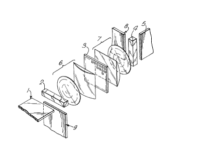
Referring to Figure 1, tllere is shown a ~irst input
array o~ inputs l formed by ~ ribbon of single mode or
multimode optical fibres located in a horizontal plane
emits light which is polarised by a polarising beam
splitter 2 and impinges upon a liquid crystal matrix arxay
3. Light passing through the liquid crystal matrix array
3 passes through an analysing polarising beam splitter 4
and thence to a ribbon of single, or ~ultimode output
fibres 5, constituting the ~irst array o~ outputs, Located
-- 6 --
in a senerally vertical plane if of the correc~
polarisation. An optical system 6 comprising a
combination o~ cylindrical and plano-convex lenses 20, 21 is
located between the beam splitter 2 and the liquid crystal
device 3 tb dlrect the light from each individual fibre ln
the xibbon l to its respective column of tne liquid
crystal device 3. lhe o:ptical system 6 and the
polarising beam splitter 2 together constitute the first
optical means. A further optical syste~ 7, also comprising a
o combination of cylindrical and plano-convex lenses 22,~4, is
located between the device 3 and the beam splitter 4.
These concentrate light ~rom a row of the matrix 3 to its
respective output ~ibre in the ribbon 5 which together
with the second polarising beam splitter 4 constitute the
second optical means. The apparatus also includes a
second array o~ input fibres 8 located in the vertioal
plane and at right angles to the output ribbon 5, and a
second array of output fibres 9 located in a vertical
plane and generally perpendicular to the input ribbon l.
The liquid crystal device 3 is typically a twisted-nematic
liquid crystal device divided into a N x N matrix, the
ribbons l, 9,5 and 8 of input and output ~ibres each
containing N fibres.
Thus considering light passing in a firs~ direction
~5 through the switch from the lnput ribbon l to the output
ribbon 5, the light is first polarised in the polariser
beam splitter 2 and any rejected light reflected from tne
interface in the beam splitter 2 upwards (in the
orientation as shown in Flgure 1). The optical system 6
spreads the non-rejected light ~rom that particular input
~lbre over a colu~n o~ cells of the liquid crystal device
3 which are in a position corresponding to that o~ the
Darti~ul~r ~hr~ in thP rihhnn ~ r~l cign~l ic
applied to one or more of the cells in the column to cause
-` ~2~ 6
a change in polarisation state of 90 degrees so that light
passing through these cells has its direction o~
polarisation rotated through 90 degrees whereas the light
passing through all of the other cells in that coiumn is
unaffected. .~he optical system 7 directs light from the
different rows of the liquid crystals de~/ice 3 towards the
ends of the respective output fibres in the ribbon 5.
However, light transmitted through cells ~hich have not
changed their polarisation state are deflected by tne
o interface of the beam splitter 4 and only light from those
cells which have been rotated through 90 degrees are
transmitted through the beam splitter to impinge upon the
end fases of the fibres in the ribbon 5.
Light passing in the opposite direction through the
switch is introduced via the optical ~ibres in the ribbon
8. Light of a particular polarisation state is reflected
~rom the interface of the beam splitter 4 and focussed by
the optical system 7 onto particular rows of the liquid
crystal device ~ corresponding to the lscation of the
optical fibres in the ribbon 8. Those cells in that
particular row which have a control signal applied to them
to cause a 90 de~ree rotation of the plane of polarisation
~or light coming from an input of the first array 1 also
will change the polarisation of light passing through it
2s from input of the second array of inputs 8. The optical
system 6 collects light from all o~ the cells and directs
it to the polarising beam splitter 2. Light which has not
had its direction of polarisation changed passes straight
through the bea~ splitter 2 ~hilst light which has has its
polarisation state changed by 90 degrees is reflected by
the inner face of the beam splitter 2 towards the ribbon
o~ output optical fibres 9. The optical system 6 focusses
the light ~rom a particular column of the liquid crystal
.~ . . .
~2~8116
- 8
device ~ onto its .espective optical fibres in the ribbon
9. Thus, once a particular channel has been established
in the opticaL switch by appl~Jing a control signal to one
particular cell of the liquid crystal device 3 two
corresponding,switch connection are made simultaneously,
one in each direction through the optical switch.
Where N = 100 a contrast ratio between light which
passes through a selected cell of the liquid crystal
device 3 and that which does not must be at least 104 or
o 40 dB. With good quality polarising beam splitters 2 and
4 and a twisted-nematic liquid crystal array this is
feas.ble.
Referring now to Fig 2, an optical switch has arrays
of inputs 1 and 8, arrays of outputs 5 and 9 and a liquid
S crystal matrix array of cells 3 as provlded in the optical
switch of Figure 1. This embodiment differs from that
shown in Figure 1 in that polarising beam splitters 10 and
11 are positioned adjacent the matrix array 3. Optical
systems 12, 13, 14 and 15 each comprising a combination of
~0 cylindrical and plano-convex lenses (illustrated
schematically as optical boxes for clarity) direct light
to or from the array 3, and to or from the inputs 1 an,d 8 and
outputs 5 and 9 ~respectively via the polariser beam
splitters. Optical systems 12, 15 and polarising beam
splitter 10, and optical systems 13, 14 and polarising
beam spl-ittèr ïï, constitute first and second optical
meàns, respectively.
The switch of Figure 2 is ~unctionally equivalent to
that of Figure 1 but with polarisation of light from an
input by a polarising beam splitter occurring after an
optical system has directed the light to be spread over
the appropriate row or column of cells, and with the light
~xom the cells being analysed by a polarising beam
... ...
_ 9 ~
splitter be~ore passing to an optical system to be applied
to an output.
The arrangement of Figure 2 having the imaging optical
components o~ each direction separated allows the output
S imaging optics of each direction to be optimised without
affecting the input optics o~ the other direction. Input
and output optics can therefore be independently
optimised. On the other hand, this configuration rPquires
a larger number of imaging devices than the con~iguration
lo of Figure 1.
Imaging optics utilising lens systems other than the
specifically described with reference to Figures 1 or 2,
or other methods such as holographic imagillg, may be
employed which distribute the input signals amongst the
cells and convey the resulting signals from the cells to
the outputs, however combinations of cylindrical and
plano-convex lenses are simple and efficient and have ~he
advantage of being freely avallable.
It will be appreciated that an optical system
according to the present invention can also be used \ for
uni-directional transmission without modification.
The optical means may include optical waveguides which
couple the light emltted from the inputs to the cells and
thence from th~ cells to the outputs. In this case the
distribution means may be formed by a number of bundles of
optical ~ibres each bundle being coupled to an input and
the fibres o~ each bundle being coupled9 respectively, to
individual cells in the group associated with that input.
In this case the geometric con~iguration o~ the active
array o~ cells may have any convenient ~orm. For example,
it may be formed by a linear or even a circular array and
may be formed by a single, multi-element component or by a
number of discrete components.
~Z9 !3~
-- 1~
Where optical waveguides replace the lens systems 6
and 7 of the embodiment of Figure l they ha~e to 3e
polarisation maintaining fibres. ~here optical wave~uides
replace the lens systems 12, 13, 14 and 15 of Figure 2 the
; ends of the waveguides will ideally be lensed to collimate
light existing the waveguides to direct it to a chosen
cell of the array 3 through the depth o~ the beam splittsr.
While the invention has been described in connection
with what is presently considered to be the most
lo practical and preferred embodiment, it is to be understood
that the invention is not to be limited to the disclosed
embodiment, but on the contrary, is intended to cover
various modifications and equivalent arrangements included
within the spirit and scope of the appended claims.
B