Note: Descriptions are shown in the official language in which they were submitted.
7~i
ELECTROPHOTOGRAPEIIC PHOTOSENSITIVE ME~ER, PROCESS
AND APPARATUS FOR THE PREPARATION THE~EOF
FIELD OF THE INVENTION
This invention relates to an improved electrophoto-
graphic ~lotosensitive member using an amorphous material,
a process and an apparatus for preparing the same.
BACKGROUND OF THE INVENTION
There have been proposed a number of~ electrophotographic
photosensitive members haviny a light receiving layer composed
of a non-crystalline material containing silicon atoms as
the main component, the so-called amorphous silicon (herein-
after referred to as "a-Si") disposed on a substrate.
And there have been proposed various methods for the
preparation of such light receiving layer for the electro-
photographic member Nsing vacuum evaporation technique, heat
chemical vapor deposition technique, plasma chemical vapor
deposition technique, reactive sputtering technique, ion
plating technique and light chemical vapor deposition technique.
Among those methods/ the method using plasma vapor
deposition technique (hereinafter referred to as "plasma
CVD method"~ has been generally recognized as being the
,. ~
,Z~ S
most preferred and is currently used to manufacture said
light receiving layer.
However, for any of the known light receiving layers,
even if it is an acceptable one that is obtained by plasma
CVD method and thatexhibits almost satisfactory character-
istics, there still remain problems unsolved in satisfying
totally the points for its characteristics, particularly
electric and optical characteristics, photoconductive
characteristics, deterioration resistance upon repeating
use and use-environmental characteristics, other points
relating to its homogeneity, reproducibility and mass-
productivity and further points relating to its lasting
stability and durability, which are required for the photo-
electric conversion layer to bè an i~novable one.
The reasons arelargely due to that the light receiving
layer can not be easily prepared by a simple layer deposition
procedure but skilled genuities are required in the process
operations in order to obtain a desirable light receiving
layer while having due regards to the starting materials.
For example, in the case of forming a film composed
of an amorphous silicon material (hereinafter referred to
as "a-Si") according to heat chemical vapor deposition
technique (hereinafter referred to as "CVD method"), after
the gaseous material containing silicon atoms being diluted,
appropriate impurities are introduced thereinto and the
~Z~ 75
thermal decomposition of related materials is carried out
at an elevated temperature between 500 and 650C.
Therefoxe, in order to obtain a desirable a-Si film by
CVD method, precise process operation and control are
required, and because of this, the apparatus in which the
process according to CVD method is practiced will be eventually
complicated and costly.
However, even in that case, it is extremely difficult
to stably obtain a desirable light receiv~ng layer composed
of an a-Si material being wealthy in practically applicable
characteristics on an industrila scale.
Now, although the plasma CVD method is widely used
nowadays as above mentioned, it is still accompanied with
problems relatiny to process operations and to facility
investment.
Regarding the former problems, the operation conditions
to be employed under the plasma CVD method are much more
complicated than the known CV~ method, and it is extremely
difficult to generalize them.
That is, there already exist a number of variations
even in correlated parameters concernin~ the temperature
of a substrate, the amount and the flow rate of gases to be
introduced, the degree of pressure and the high frequency
power for forming a layer, the struc~ure of an electrode,
the structure of a reaction chamber, the flow rate of gases
~ - \
~Z~7~
to be exhausted, and the plasma generation system. Besides
said parameters, there also exist other kinds of parameters.
Under these circumstances, in order to obtain a desirable
deposited film product it is required to choose precise
parameters from a great nurnber of varied parameters. And
sometimes serious problems occur. For instance, because
of the precisely chosen parameters, a plasma is apt to be
in an unstable state which invites problems in a deposited
film to be formed~
And for the apparatus in which the process using the
plasma CVD method is practiced, its structure will be eventually
complicated since the parameters to be employed are precisely
chosen as above stated. Whenever the scale or the kind of
the apparatus to be used is modified or changed r the apparatus
must be so structured as to cope with the precisely chosen
parameters.
In this regard, even if a desirable deposited film
should be fortuitously mass-produced, the film product
becomes unavoidably costly because (1) a heavy investment
is firstly necessitated to set up a particularly appropriate
apparatus therefor ; (2) a number of process operation
parameters even for such apparatus still exist and the
relevant parameters must be precisely chosen from the existing
various parameters for the mass-production of such film. In
accordance with such precisely chosen parameters, the process
must then be carefully practiced.
~Z913~7~
Against this background, an electrophotographic photo-
sensitive member has become diversified nowadays. And
there is an increased demand to stably provide a relatively
inexpensive electrophotographic photosensitive member having
a light receiving layer with a normal square measure or a
large square measure composed of an a-Si material which has
a relevant uniformity and many applicable characteristics
and which is suited for the use purpose and the application
object.
Consequently, there is an earnest desire to develop
an appropriate method and apparatus to satisfactorily meet
the above demand.
Likewise, there is a similar situation which exists
with respect to other kinds o.~ non-.monocrystalline light
receiving layers for electrophotographic photosensitive
member, for example, those composed of an a-Si material
containing at least one kind selected from oxygen atoms,
carbon atoms and nitrogen atoms [hereinafter referred to as
"a-Si(H,X)(O,C,N)"].
SU~L~IARY OF THE INVENTION
The present inventors have conducted extensive studies
in order to solve the problems in the aforementioned known
methods and in order to develop a new process for effectively
~LZ9~3~75
and simply preparing an improved electrophotographic photo-
sensitive member having a desirable light receiving layer
composed of a non-crystalline semiconducting material, which
has a wealth of practically applicable characteristics,
without depending upon any known method and which meets the
above-mentioned demands.
As a result, the present inventors finally have found
a process that enables one to efficiently and stably prepare
said electrophotographic photosensitive member in simplified
particular procedures as detailed below.
It is therefore an object of this invention to provide
an improved electrophotographic photosensitive member provided
with a desirable light recei~ing layer composed of a non-
crysta]line material which has many practically applicable
characteristics and brings about excellent electrophotographic
functions, and which is prepared without depending upon
plasma reaction.
Another object of this invention is to provide a process
for preparing the improved electrophotographic photosensitive
member by which the light receiving layer can be mass-produced
with simplified film forming conditions in a film forming
space without plasma discharge while maintaining the character-
istics of the film to be formed and promoting the film-forming
rate.
A further object of this invention is to provide an
1~8~7~
apparatus suitable for practicing the present process.
These and other objects, as well as the features of
-this invention will become apparent by reading the following
descriptions of preferred embodiments according to this
invention while referring to the accompanying drawinys.
BRIEF DESCRIPTION OF THE DRAWINGS
Figure l(A) through Figure l(F) are schematic portion
views for illustrating representative embodiments of an
electrophotographic photosensitive member according to this
invention, in which Figure l(A) is a cross-sectional view of
a first representative embodiment of an electrophotographic
photosensitive member according to this invention;
Figure l(B) is a cross-sectional view of a second
represen-tative embodiment of an electrophotographic
photosensitive member according to this invention;
Figure l(C) is a cross-sectional view of a third
representative embodiment of an electrophotoelectric
photosensitive member according to this invention;
Figure ltD) is a cross-sectional view of a fourth
representative embodiment of an electrophtoelectric
photosensitive member according to this inven~ion;
Figure l(E) is a cross-sectional view of a fifth
representative embodiment of an electrophotographic photo-
~?c~ - 7 --
3.2~8~L~S
sensitive member according to this invention; and
Figure l(F) is a cross-sectional view o~ a sixth
representative embodiment of an electrophotographic photo-
sensitive member according to this invention.
Figure 2(A) through 2(C) are schematic diagrams of a
representative apparatus for practicing the process for
preparing an electrophotographic photosensitive member
according to this invention, in which
'Figure 2(~) is a schematic cross-sectional view of the
apparatus; Figure 2(B) is a schematic longitudinal-sectional
view of the apparatus; and Figure 2(C) is a schematic
longitudinal-sectional view of the gas transport'ing conduit
of the apparatus.
Figure 3 is a schematic diagram of another representative
appar~tus ~or practi~ing the process for prepar~ng an electro-
....
photographic photosensitive member according to this invention.
DESCRIPTION OF THE INVENTION
The present inventors have made earnest studies for,overcoming the foregoing problems on the conventional electro-
photographic photosensitive member and attaining the objects
as described above and, as a result, have accomplished this
invention based on the findings as described below.
That is, (i) a substance which can be a constituent
.. 8
lZ9~7S
for forming a photoelectric conversion layer but which does
not or can hardly contribute to form said layer as long as
it remains in its original energy state and ~ii) another
substance which can react with the substance (i) to electron-
ically oxidize it (which means that the atom, ion or molecule
of the substance loses an electron, namely the oxidation
number is increased) were selected, and the two substances
(i) and (ii) in gaseous state were separately introduced
through respective transporting passage into a film forming
space wherein a substrate for the electrophotographic photo-
sensitive member being maintained at about 300C is placed
to thereby let the two substances (i) and (ii) collided and
contacted to occur a mutual reaction among the two substances
(i.) and (ii) in the space positioned over the substrate in
the film forming space.
As a result, there was formed a homogeneous deposited
film with a uniorm thickness without accompaniment of
any solid particle on the substrate. And it was found that
the resulting deposited film has a wealth of electric and
optical properties and is uniformly accompanied with an
excellent electrophotographic function.
With an electrophotographic photosensitive member was tried
to prepare in accordance with the above procedures, there was
obtained a desirable electrophotographic photosensitive
member having a light receiving layer which is wealthy in
practical applicable characteristics such as electric and
optical characteristics, deterioration resistanc~ upon
repeating use and use-environmental characteristics and
which has an excellent electrophotographic function. As
a xesult, it was confirmed that this method is of a sufficient
repeatability.
This invention has heen completed based on these findings,
and it includes an improved electrophotographic photosensitive
member, a process and an apparatus for preparing the same.
That is, according to one aspect of this invention,
there is provided an improved electrophotographic photosensitive
member comprising a substxate for electrophotography and a
light receiving layer disposed on the surface of the substrate,
the light receiving layer being a layer which was formed by
introducing (i) a substance whi.ch can be a constituent for
forming a deposited film but which does not or can hardly
contribute to form said film as long as it remains in its
original energy state (hereinafter referred to as "substance
A") in gaseous state and a gaseous substance ha~ing a property
to electronically oxidize the substance (hereinafter referred
to as "o~idizing agent") separately through respective gas
transporting space into a film forming space wherein the
substrate is placed while being maintained at predetermined
temperature, making the two substances contacted each other
in the absence of a plasma in the space positioned above the
3L2~ 7~
surface of the substrate to thereby generate plural kinds
of precursors containing excited precursors and let at
least one kind of those precursors directed to form said film.
According to another aspect of this invention, there is
provided a process for preparing an improved electrophoto-
graphic photosensitive member, characterized; (a~ employing
together a gaseous substance A and a gaseous oxidizing agent,
(b) passing the gaseous suhstance A through a transportation
space leading a film forming space wherein a substrate for electro-
photogr-aphy i-s-.pl-.ac~d wh,i~e b~ing maintained at a predetermined
temperature, (c) passing the gaseous oxidizing agent through
the other transportation space leading to the film forming
space and (d) contacting the substance A and the oxidizing
agent in the absence of a plasma in the space positioned
above the surface of the substrate to thereby generate plural
kinds of precursors containing excited precursors and let at
least one kind of those precursors directed to form a deposited
film to be a light receiving layer for said electrophotographic
photosensitive member.
According to a further aspect of this invention, there
is provided an apparatus suitable for practicing the above
process which comprises a double conduit having an outer
passage for the gaseous oxidizing agent and an inner passage
for the gaseous substance A and a film forming chamber having
a supporting means for a substrate for the electrophotographic
~8~7S
photosensitive member.
According to this invention, there can be obtained
a desirable light receiving layer for the electrophotographic
photosensitive member in the absence of a plasma without
having any influence of plasma etching or any problem due to
abnormal discharge actions since the process does not depend
upon the conventional plasma CVD method using a gaseous
plasma formed by subjecting the starting gaseous materials
to the action of a discharge energy.
In addition, according to this invention, there are
provided the following advantages; a desirable light receiving
layer for an electrophotographic photosensitive member
having a uniform thickness and a desirable homogeneity may
be effectively formed at an improved film forming rate in
simple procedures without consumption of so much energy as
in the conventional plasma CV~ method; the operation param-
eters for preparing a light receiving layer for an electro-
photographic photosensitive member may be largely simplified;
an improved electrophotographic photosensitive men~er having
such desirable light receiving layer or if necessary, of
a large square measure may be mass-produced on an industrial
scale to thereby reduce the cost of a product; and such a
heavy investment as much for the apparatus in the conventional
plasma CVD method is not necessitated even in the case of
setting up a particularly appropriate apparatus to practice
~Z~ 75
the process of this invention.
DESCRIPTION OF THE PREFERRED E~ODIMENTS
Representative embodiments of the electrophotographic
photosensitive member, the process and the apparatus for
the preparation of the same according to this invention
will now be explained more specifically referring to the
drawings. The description is not intended to limit the
scope of the invention.
The electrophotographic photosensitive members provided
according to this invention are represented by those shown
in Figure l(A) through l(F).
Figure l(A) is a cross-sectional view of a irst
representative embodiment of an electrophotographic photo-
sensitive member according to this invention;
Figure l(B) is a cross-sectional view of a second
representative embodiment of an electrophotographic photo-
sensitive member accordiny to this invention;
Figure l(C) is a cross-sectional view of a third
representative embodiment of an electrophotoelectric photo-
sensitive member according to this invention;
Figure l(D) is a cross-sectional view of a fourth
representative embodiment of an electrophotoelectric photo-
sensitive member according to this invention;
Figure l(E) is a cross-sectional view of a fifth
representative embodiment of an electrophotographic photo-
sensitive member according to this invention; and
Fi~ure l(F) is a cross-sectional view of a sixth
representative embodiment of an electrophotographic photo-
sensitive member according to this invention.
In any of the above electrophotographic photosensitive
members, the substrate may be either electroconductive or
electrically insulative.
The electroconductive substrate can include, for example,
metals such as NiCr, stainless steel, Al, Cr, Mo, Au, Nb,
Ta, V, Ti Pt, and Pb, or the alloys thereof.
The electrically insulative substrate can include, for
example, film or sheet of synthetic resins such as polyester,
polyethylene, polycarbonate, cellulose acetate, polypropylene,
polyvinyl chloride, polyvinylidene chloxide, polystyrene, and
polyamide; glass, ceramics, and paper. It is preferred that
the electrically insulative substrate is applied with electro-
conductive treatment to at least one of the surfaces thereof
and disposed with a light receiving layer on the thus txeated
surface.
In the case of glass, for instance, electroconductivity
is applied by disposing, at the surface thereof, a thin film
made of NiCr, Al, Cr, ~o, Au, Ir, Nb, Ta, V, Ti, Pt, Pd, In202,
SnO3, ITO (In203 + SnO2), etc. In the case of the synthetic
14
7Si
resin film such as polycarbonate film, the electroconductivity
is provided to the surface by disposing a thin film of metal
such as NiCr, Al, ~g, Pb, Zn, Ni, Au, Cr, Mo, Ir, Nb, Ta, V,
Tl, and Pt by means of vacuum deposition, electron beam vapor
deposition, sputtering, etc. or applying lamination with the
metal to the surface. The substrate may be of any configuration
such as cylindrical, belt-like or plate-like shape, which can
be properly determined depending on the applications. For
instance, it is desirably configurated into an endless belt
or cylindrical form in the case of continuous high speed
production. The thickness of the substrate is properly
determined so that the light receiving layer as desired can
be formed. In the case where flexibility is required for
the electrophotographic photosensitive member, it can be
made as thin as possible within a range capahle of sufficiently
providing the function as the substrate. ~owever, the thickness
is usually greater than 10 ~m in view of the fabrication and
handling or mechanical strength of the support.
The first embodiment [Figure l(A)]
The electrophotographic photosensitive member comprises
a single light receiving layer 102 disposed on the substrate
101 .
The single light receiving layer 102 is composed of
an a-Si material! preferably, an a-Si material containing,
, . . . , ~
7~;
in addition to silicon atoms, at least one kind selected from
hydrogen atoms (H) and halogen atoms (X) [hereinafter referred
to as "a-Si(H,X)"].
The halogen atom (X) contained in the light rece,iving
layer 102 include, specifically, fluorine, chlorine, bromine
and iodine, fluorine and chlorine being particularly preferred.
The amount of the hydrogen atoms (H), the amount of the
halogen atoms (X) or the sum of the amounts for the hydrogen
atoms and the halogen atoms (H+X) contained in the light
receiving layer 102 is usually from 1 to 40 atm ~ and,
preferably, from 5 to 30 atm %.
It is possible for the above light receiving layer 102
to further contain germanium atoms (Ge) and~or tin atoms (Sn).
In the case where the above light receiving layer 102
is composed of an a-Si(H,X) material containing germanium
atoms (Ge) and/or tin atoms (Sn) [hereinafter referred to
as "a-Si(Ge,Sn)(~I,X)"~, there is provicled an improvement
in the absorption spectrum characteristics in the long wave-
length region of the light receiving layer.
That is, incorporating at least one kind selected from
germanium atoms and tin atoms into the light receiving layer
becomes to brin~ about a desired electrophotographic photo-
sensitive member which is more sensitive to light of wavelengths
broadly rangingfrom short wavelength to long wavelength
covering visible light then quickly responsive to light.
16
- - ~
~2~38~ 7S
This effect becomes more significant when a semiconductor
laser emitting ray is used as the light source.
The amount of germanium atoms and/or tin atoms in the
light receiving layer 102 should be properly determined
so that the object of the invention is effectively achieved.
It is usually 1 to 6 x 10 atomic ppm, preferably 10 to
3 x 10⁵ atomic ppm, and more preferably 1 x 10 to 2 x 10⁵
atomic ppm.
It is also possible for the above light receiving layer
102 to contain a substance for controlling the conductivity.
As such substance, the so-called impurities in the
filed of the semiconductor can be mentioned and those usable
herein can include atoms belonging to the group III of the
periodic table that provide p-type conductivity (hereinafter
simply referred to as "group III atoms") or atoms belonging
to the group V of the periodic table that provide n-type
conductivity (hereinafter simply referred to as "group V
atoms"). Specifically, the group III atoms can include
B (boron), Al (aluminum), Ga (gallium), In (indium) and Tl
(thallium), B and Ga being particularly preferred. The group
V atoms can include, for example, P (phosphorus), As (arsenic),
Sb (antimony), and Bi (bismuth), P and Sb being particularly
preferred.
In the case ~Ihere either the group III or the group V
atoms are incorporated into the light rece}ving layer 102,
7S
there is provided an electrophotographic photosensitive
member having a light receiving layer of which the type of
conductivity and the conductivity are appropriately controlled.
The amount of either the group III or the group V in the
light receiving layer 102 in that case is preferably from
1 x 10 3 to 1 x 10³ atomic ppm, more preferably, from 5 x 10 2
to 5 x 10 atomic ppm, and, most preferably , from 1 x 10 1
to 5 x 10² atomic ppm.
The second to sixth embodiments [Figure l(B) through Figure l(F)]
In any of these cases, the light receiving layer is of
a multi-layered structure and has a photosensitive layer 103
as one of the constituent layers.
The photosensitive layer 103 may be the same as the light
receiving layer 102 of the first embodiment as shown in
Figure 1(~).
That is, in the second to sixth embodiments shown in
Figure l(B) through Figure l(F), the photosensitive layer 103
is composed of an a-Si(H,X) material or an a-Si(Ga,Sn)(H,X)
material, if necessary, containing either the group III or
the group V atoms.
Referring Figure l(B), the electrophotographic photosensitive
member comprises the substrate 101 and a light receiving layer
102 constituted by a layer 104 containing a substance for
controlling the conductivity and the photosensitive layer 103.
18
:~LZ~ 17S
In this embodiment, the layer 104 contains a relatively
large amount of the substance for controlling the conductivity,
namely, either the group III or the group V atoms and functions
as a charge injection inhibition layer.
That is, i~ the case of incorporating the group III or
group V atoms in a uniformly distributed state to a portion
of the layer region in contact with ~he support, or the
atoms are contained such that the distribution density of
the group III or group V atoms in the direction of the layer
thickness is higher on the side adjacent to the support, the
constituting layer containing such group III or group V atoms
or the layer region containing the group III or group V atoms
at high concentration function as a charge injection inhibition
layer. That is, in the case of incorporating the group III
atoms, movement of electrons injected from the side of the
support into the photosensitive layer can effectively be
inhibited UpOIl applying the charging treatment of at positive
polarity at the free surface of the photosensitive layer.
While on the other hand, in the case of incorporation the
group III atoms, movement of positive holes injected from the
side of the support into the photosensitive layer can effectively
be inhibited upon applying the charging treatment at negative
polarity at the free surface of the layer. The content in
this case is relatively great. Specifically, it is generally
from 30 to 5 x 10⁴ atomic ppm, preferably from 50 to 1 x 10
19
~L2~75
atomic ppm, and most suitably from 1 x 10 to 5 x 10³ atomic
ppm. Then, for the charge injection inhibition layer to
produce the intended effect, the thickness (T) of the photo-
sensitive layer and the thickness (t) of the layer or layer
region containing the group III or group V atoms adjacent to
the support should be determined such that the relation
t/T _ 0.4 is established. I~ore preferably, the value for the
relationship is less than 0.35 and, most suitably, less than
0.3. Further, the thickness (t) of the layer or layer region
is generally 3 x 10 3 to 10 ~m, preferably 4 x 10³ to 8 ~m,
and, most suitably, 5 x 10 3 to 5 ~m.
The distribution state of the group III or group V atoms
and the amount o~ the group III or group V atoms are, of
course, combined properly as required for obtaining the
light receiving member having performanees capable of
attaining a desired purpose. For instanee, in the case of
disposing the eharge injeetion inhibition layer at the end
of the photosensitive layer on the side of the support, a
substance for eontrolling the conductivity of a polarity
different from that of the substance for controlling the
eonductivity eontained in the eharge injection inhibition
layer may be contained in the photosensitive layer other
than the charge injection inhibition layer, or a substanee
for controlling the conductivity of the same polarity may
be contained by an amount substantially smaller than that
~ %~.7~
contained in the charge inhibition layer.
~ eferring Figure l(C), the electrophotographic photo-
sensitive member comprises the substrate 101 and a light
receiving layer 102 constituted by an intermediate layer
105 containing at least one kind selected from oxygen atoms,
carbon atoms and nitrogen atoms and the photosensitive
layer 103.
In this embodiment, the intermediate layer 105 is
composed of an a-Si(H,X~ material containing at least one
kind selected from oxygen atoms, carbon atoms and nitrogen
atoms [hereinafter referred to as "a-Si(O,C,N)(H,X)"].
This is effective in increasing the photosensitivity
and dark resistance of the light receiving layer and in
improving adhesion between the substrate and the light receiving
layer. ~.
And, since the intermediate layer 105 is also effective
in efficiently preventing inflow of photocarriers from the
side of the substrate 101 into the photosensitive layer 103
and in promoting movement of the photocarriers, which are
generated in the photosensitive layer 103 and moved toward
the substrate 101, from the side of the photosensitive layer
103 toward the substrate 101, it functions as a barrier layer.
The amount of at least one kind selected from oxygen
atoms, carbon atoms, and nitrogen atoms contained in the
intermediate layer 105 is determined while considering the
~L2~8~175
organic relationship such as the performance at the interface
in contact with the substrate, in addition to the performance
required for the light receiving layer, and it is preferably
from 0.001 to 50 atomic %, more preferably, from 0.002 to
40 atomic ~, and, most preferably, from 0.003 to 30 atomic %.
The thickness of the intermediate layer 105 is preferred
to be less than 5 ~m.
Further, the intermediate layer 105 may become to function
as a charge injection inhibition layer by incorporating either
the group III or the group V atoms thereinto.
Referring Figure l(D), the electrophotographic photo-
sensitive member comprises the substrate 101 and a light
receiving layer constituted by the photosensitive layer 103
and a surface layer 106 having a free surface.
In this embodiment, the surface layer 106 is composed of
an a-Si(~,X) material containing at least one kind selected
from oxygen atoms (O), carbon atoms (C) and nitrogen atoms (N)
in a uniformly distributed state [hereinafter referred to
as "a-SilO,C,N)(H,X)"].
The surface layer 106 is disposed to the photosensitive
layer 103 with an aim of improving the moisture-proofness,
performance for continuous repeating use, electrical voltage
withstanding property, circumstantial resistant property
and durability, and these purposes can be attained by
incorporating at least one kind selected from oxygen atoms,
22
:~L2~8~.75
carbon atoms and nitrogen atoms in the amorphous material
constituting the surface layer.
At least one kind selected from oxygen atoms, carbon
atoms and nitrogen atoms are contained in a uniformly
distributed state in the surface layer 106, by which the
foregoing various properties can be improved in accordance
with the increase in the content of such atoms. However, if
the content is excessive, the layer quality is reduced and
electrical and mechanism properties are also degraded. In
view of the above, the amount of such atoms is preferably
from 0.001 to 90 atm %, more preferably, from 1 to 90 atm~%
and, most preferably, from 10 to 80 atm %.
The surface layer 106 has to be formed with an utmost
care so as to obtain the properties as desired. That is,
the state of the substance comprising silicon atoms, oxygen
atoms and, further, hydrogen atoms and/or halogen atoms as
the constituent atoms is from crystalline to amorphous
state/ the electrical property of the layer may vary from
the conductive, to semiconductivity and insulating property
and/ further, the photoelectronical property of the layer
may also vary from photoconductive to non-photoconductive
property depending on the content of each of the constituents
atoms and other conditions of preparation. Accordingly,
it is essential to select the content for each of the
constituents atoms and the preparation conditions such
~2~l75
that the surface layer 106 having desired properties depending
on the purpose can be formed.
For instance, in the case of disposing the surface
layer 106 mainly for improving the electrical voltage
withstanding property, the amorphous material constituting
the surface layer 106 is formed such that it exhibits
remarkable electrically insulating behaviors under the
working conditions. Further, in the case of disposing the
surface layer 106 mainly for improving the properties in
the continuous repeating use or the circumstantial-resistant
property, the amorphous layer constituting the surface
layer 106 is formed such that the layer has a photosensitivity
to some extent to the irradiated light, although the degree
of the electrically insulating property is somewhat moderated.
The thickness of the surface layer is also one of the
important factors for effectively attaining the purpose
of this invention and it is properly determined depneding
on the desired purposes. It is, however, also necessary
that the layer thickness is determined in view of relative
and organic relationships in accordance with the amounts
of the oxygen atoms, carbon atoms, nitrogen atoms, halogen
atoms and hydrogen atoms contained in the layer or the
properties required for the surface layer. Further, it
should be determined also in economical point of view such
as productivity or mass productivity. In view of the above,
24
~ \
~L2~ 5
the thickness of the surface layer 106 is preferably from
3 x 10 3 to 30 ~, more preferably, from 4 x 10 3 to 20
and, most preferably, from 5 x 10 3 to 10 ~.
~ eferring Figure l(E), the electrophotographic photo-
sensitive member comprises the substrate 101 and a light
receiving layer 102 constituted by the charge injection
inhibition layer 10~, the photosensitive layer 103 and the
surface layer 106.
Referring ~igure l(F), the electrophotographic photo-
sensitive member comprises the substrate 101 and a light
receiving layer 102 constituted by a first layer 107 contain-
ing at least one kind selected from germanium atoms tGe)
and tin atoms (Sn) and a second layer 108 containing neither
germanium atoms nor tin atoms.
That is, the first layer 107 is composed of an a-Si
(Ge,Sn)(H,X) material and the second layer 108 is composed
of an a-Si(H,X) material.
The electrophotographic photosensitive member of the
type as shown in Figure l(F) becomes to give excellent
various properties by incorporating germanium atoms and/or
tin atoms in the first sensitive layer 107. Particularly,
it becomes more sensitive to light of wavelengths broadly
ranging from short wavelength to long wavelength covering
visible light and it also becomes quickly responsive to
light.
This effect becomes more significant when a semiconductor
laser emitting ray is used as the light source.
The formation of a relevant light receiving layer 102
as explained above on the substrate 101 to prepare the
electrophotographic photosensitive member is carried out
in accordance with the foregoing procedures in which the
corresponding substance A and the oxidizing agent are
appropriately selected and used.
That is, in the case of forming the layer composed of
a-Si(H,X) material, a gaseous or gasifiable silicon hydride
(silane) such as SiH4, Si2H6, Si3H8 and Si4Hlo or a gaseous
or gasifiable halogen-substituted silicon hydride (halogenated
silane) such as SlH3Cl, SiH3F and SiH3Br may be preferably
used as the starting substance A.
And as the oxidizing agent in that case, a halogen gas
such as F2, C12, Br~ and I2 or a nascent state halogen such
as nascent state fluorine, chlorine and iodine may be
preferably used. And among these substances, F2 gas and
C12 gas are most preferred.
In the case of forming the layer composed of a-Si
(Ge,Sn)(H,X) material, a gaseous or gasifiable substance for
introducing germanium atoms or a gaseous or gasifiable
substance for introducing tin atoms is selectively used
in addition to the above silane gas or halogenated silane
gas.
26
~Z9~3 IL7~
, . .
The substance for introducing germanium atoms can
4, Ge2H6, Ge3H8, Ge4HlO and Ge5H12 As the
substance for introducing tin atoms, there are, for example,
tin hydrides such as SnH4.
As the oxidizing agent, any of the foregoing oxidizing
agents can be used. And ~e gas or C12 gas can be most
preferably used.
In the case of forming the layer composed of a-Si(H,X)
containing the group III or the group V atoms or the layer
composed of a-Si(Ge,Sn)(H,X) containing the group III or
the group V atoms, in addition to the above mentioned
substance A to be used in the formation of the layer
composed of a-Si(H,X) or the layer composed of a-Si(Ge,Sn)(H,X),
a gaseous substance containing the group III or the group V
atoms as the constituent element is selectively used. And
as the oxi~izing agent to be used in this case, the same
substance as used in the above case is used.
Spec~fically, usable as the gaseous substance for the
group III atoms are, B2~16~ B4Hlo~ BsHg, B6 10' 6 12 3 3
Al(C2H5)3, Ga(CH3)3 and In(CH3)3. Among these compounds,
B2H6 is most preferred.
Usable as the gaseous substance for the group V atoms
are~ for example~ PH3~ P2H4~ AsH3~ SbH3 and BiH3- Among
these compounds, PH3 is most preferred.
The gaseous substance either for the group III atoms
-" ~2~ 75
or for the group V atoms is introduced into a film forming
space solely or together with the gaseous substance A
such as SiH4 or Si2H6, chemically contacted with the
separately introduced gaseous oxidizing agent therein.
And the gaseous substance A and the gaseous substance
either for the group III atoms or for the group V a~oms
are activated by the action of the oxidizing agent to
generate plural kinds of precursors containing excited
precursors.
Further, in the case of forming the layer composed of
a-Si(O,C,N)(H,X), in addition to the foregoing gaseous silane
such as SiH4 or Si2H6 or the foregoing gaseous halogenated
sllane such as SiH3Cl, SiH3F or SiH3Br to be used as the
gaseous substance A in the case of forming the layer composed
of a-Si(H,X), there is used a gaseous or gasifiable nitrogen
compound such as nitorgen (N2), ammonia (NH3), hydrazine
(H2NNH2), hydrogen azide (HN3) and ammonium azide (NH4N3) or
a carbon atom containing compound such as saturated hydrocarbons
of 1 to 4 carbon atoms, ethylenic hydrocarbons of 2 to 4
carbon atoms and acetylenic hydrocarbons of 2 to 3 carbon
atoms.
Specifically, the saturated hydrocarbons can include
methane (CH4), ethane (C2H6), propane (C3H8), n-butane
(n-C4H10) and pentane (C5H12), the ethylenic hydrocarbons
can include ethylene (C2H4), propylene (C3H6), butene-l
~2~ S
(C4H~), butene-2 (C4H8), isobutylene (C4H8) and pentene
(C5Hlo) and the acetylenic hydrocarbons can include
acetylene (C2H2), methylacetylene (C3H4) and butine
(C4H6) .
And as the gaseous oxidizing agent, there is used an
oxygen containing gas such as air, oxygen (2) and ozone
(03), a gaseous nitrogen oxide such as dinitrogen oxide
(N20), dinitrogen trioxide (N203) and dinitrogen tetraoxide
(N204), a peroxide such as hydrogen peroxide (H202), halogen
gas such as F2, C12, Br2 and I2, or a nascent state halogen
such as nascent state fluorine, chlorine and iodine.
E`urther in addition, in the case of forming the layer
composed of a-Si(O,C,N)(H,X) containing either the group
III atoms or the group V atoms, in addition to those gaseous
substances to be used as the gaseous substance A in the
above case of forming the layer composed of a-Si(O,C,N)(H,X),
there is used the gaseous substance either for the group III
atoms or for the group V atoms such as B2H6 gas or PH3 gas.
As the gaseous oxidizing agent, the above mentioned
oxygen containing gas, gaseous nitrogen compound, halogen
gas can be optionally usedO
In the process for preparing an improved electrophoto-
graphic photosensitive member according to this invention,
the conditions upon forming the photosensitive layer and
other layers, for example, the combination of the gaseous
29
substance A with the gaseous oxidizing agent, their mixing
ratios, the gas pressure upon mixing those substances in
the film forming space, their gas flow rates, the internal
pressure upon forming a layer on the substrate, the carrier
gas flow rate, the temperature of the substrate and the
flow type of each gaseous substance when introduced into the
film forming space are important factors for obtaining an
appropriate having desired characteristics and they are
appropriately selected while considering the functions of
the layer to be formed. Further, since these layer for~ing
conditions are organically correlated and may be varied
depending upon the kind and the amount of each of the atoms
contained in the layer, the conditions are to be determined
takin~ these relationships into consideration.
The volume ratio of the starting substance A to the
electronically oxidizing agent on the basis of the flow
ratio is preferably 1/100 to 100/1, and more preferably,
1/50 to 50/1.
As for the volume ratio of the gaseous substance for
controlling the conductivity to the gaseous substance A
on the basis of the flow ratio is preferably 1/106 to 1/10,
more preferably, 1/105 to 1/20, an~ most preferably, 1/105
to 1/50.
The gas pressure in the film forming space when the
gaseous substance A is mixed with the gaseous oxidizing
~298~l~S
agent is preferred to be higher in order to facilitate
their chemical contact. But it is necessary to be
determined with due -regard to their reactivities.
Therefore, it is preferably 1 x 10 7 to 10 atmospheric
pressure, and more preferably, 1 x 10 6 to 3 atmospheric
pressure.
The internal pressure in the film forming space, namely,
the pressure of the inner space wherein the substrate is
placed is appropriately determined with due regard to the
excited precursors to be generated in the above inner space
and to the conditions which let those precursors derived from
the excited precursors to become effective in forming a
deposited layer.
The internal pressure in the film forming space in the
case where the reaction region is open-connected to the film
forming region can be adjusted with the use of a differential
exhausting means or a large scale exhausting device while
having due regard to the correlated conditions relating to
the introducing pressure and the introducing flow rate for
each of the gaseous substance A, the gaseous oxidizing agent
and the gaseous substance for controlling the conductivity
when they are introduced into the reaction region of the film
forming space.
In the case where the conductance of the connecting
part between the reaction region and the film forming
``` ~2~ S
reginn i~ relatively small, the internal pressure in the
film forming region can be adjusted by controlling the
amount of the exhausting gas by operating an exhausting
device being connected to the film forming region.
Further in the case where the reaction region and the
film forming region are united and they are not structurally
separated, it is desirable to conduct the gas exhaustion
with a differential gas exhausting means or with the use of
a large scale gas exhausting device.
As above mentioned, the internal pressure in the film
forming space is determined while having a due regard on the
correlative pressure conditions in introducing the gaseous
substance A, the gaseous oxidizing agent and the substance
for controlling the conductivity into the film forming space.
However, in general, the internal pressure is preferably,
0.001 to 100 Torr, more preferably, 0.01 to 30 Torr, and most
preferably, 0.05 to 10 Torr.
As for the form of the gas flow into the film forming
space for each of the foregoing substances, they are
appropriately designed with due regard to the geometrical
arrangement of the gas flow inlet, the substrate and the
gas flow outlet so that the gaseous substance A, the gaseous
oxidizing agent and the substance for controlling the
conductivity can be effectively introduced into and homoge-
neously and well mixed in the predetermined region of the
32
~2~
film forming space to generate desired precursors and to
bring about the effective formation of a deposited film
on the substrate.
The temperature of the substrate upon forming a
d~posited film thereon is properly determined according
to the kind of a gaseous substance to be employed and also
to the kind of a deposited film to be formed.
That is, in the case of forming a deposited film
composed of an amorphous material, it is preferably room
temperature to 450C, more preferably, 50 to 450C, and,
most preferably, 70 to 350C.
The atmospheric temperature in the film forming space
is properly determined with due regard to the temperature
of the substrate so that desired precursors are effectively
generated, and those precursors as generated and other
precursors derived from the former precursors are not changed
into undesired things during the film forming process in the
film forming space.
Now, description will be hereunder made on an apparatus
suitable for practicing the above process for preparing an
improved electrophotographic photosensitive member according
to this invention referring to the drawings. But the
description is not intended to limit the scope of the invention.
Figures 2(A) through 2(C) are schematic diagrams of
a representative apparatus for practicing the process for
preparing an electrophotographic photosensitive member
according to this invention, in which
Figure 2~A) is a schematic cross-sectional view of the
apparatus; Figure 2(B) is a schematic longitudinal-sectional
view of the apparatus; and Figure 2(C) is a schematic
longitudinal-sectional view of the gas transporting conduit
of the apparatus.
Figure 3 is a schematic diagram of another representative
apparatus for practicing the process for preparing an electro-
photographic photosensitive member according to this invention.
Referring Figure 2(A) to Figure 2(C), film forming
chamber 201 has a film forming space C in which substrate
holder 211 for substrate 210 in the drum form having
electric heater 211' being connected to power source with
lead wires (not shown).
The film forming chamber 201 is provided with exhaust
pipe 213 being connected through main valve 214 serving to
break vacuum in the film forming chamber to an exhaust device
~not shown).
Double conduit 204 has gaseous substance A transporting
conduit 205 horizontally installed at the middle and gaseous
oxidizing agent transporting conduit 202 horizontally provided
with the circumferential wall. The double conduit has
gaseous oxidizing agenttransporting space B between the
inner wall face of the conduit 202 and the outer wall face
34
~2~ 7S
of the conduit 205. The conduit 205 is open at ^ne end
adjacent to mixing region B' being situated at the downctream
side and connecte~ to the film forming space A through nozzle
means or orifice means 212.
The holder 211 for the substrate 210 is suspended from
the upper wall of the film forming chamber 201 through rotary
shaft 215 being mechanically connected to motor 212 so that
the holder 211 can be rotated, lifted or descended by the
action of the rotary shaft 215.
The conduit 202 has the plural number gas liberation
holes 203 with the inner wall.
The position of the opening 205' of the conduit 205
is situated about 1 to 5 cm distance from the nozzle means
213.
Feeding pipe 206 of the gaseous substance A from a
reservoir (not shown) is connected to the conduit 205 through
valve means 205'. Feeding pipe 209 of carrier gas is
connected to the pipe way of the feeding pipe 206. Feeding
pipe 203 of the gaseous oxidizing agent is connected to the
conduit 202 through valve means 207'.
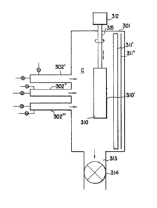
Referring Figure 3, there is shown another representative
apparatus for practicing the process for preparing an electro-
photographic photosensitive member,according to this invention
which is provided with three double conduits 302', 302" and
302ll respectively being of the same structure as the double
lZ~ 7S
conduit 204 shown in Figure 2(A) through Figure 2(C).
Every double conduit is open at one end to film forming
space B of film forming chamber 301 through an appropriate
nozzle means (not shown) as in the apparatus shown in
Figure 2(A) throuyh Figure 2(C).
~ ol.der 310 for substrate 310' in the drum form is
suspended from the upper wall of the film forming chamber
301 through rotary shaft 315 being mechanically connected
to motor 312 so that the holder 310 can be rotated, lifted
or descended by the action of the rotary shaft 315.
The film forming chamber 301 is provided with exhaust
pipe 313 being connected through main valve 314 serving to
break vacuum in the film forming chamber to an exhaust device
(not shown).
In the film forming chamber 301, there are longitudinally
install infrared lamp 403 for heating the substrate 310' and
mirror 311' reflecting the infrared radiation toward the
substrate 310'.
The advantages of this invention are now described in
more detail by reference to'the foIlowing Examples, which
are provided here for illustrative purposes only, and are
not intended to limit the scope of this invention.
Example 1
An electrophotographic photosensitive member having
a charge injection inhibition layer~ a photosensitive layer
12~ 7~i
and a surface layer or a substrate of the type as shown in
Figure l(E) was prepared using the apparatus shown in Figure
2(A) through Figure 2(C).
In this example, the position of the opening 205' of
the conduit 205 is adjusted to be about 3 cm distance from
the surface of the substrate 210.
An alminum cylinder for electrophotography was used
as the substrate 210, and it was firmly disposed onto the
holder 211.
The vacuum in the film forming chamber was brought to
and maintained at about 10 5 Torx by regulating the exhaust
valve 214.
Then the heater 211' was ignited to heat the cylinder
and it was maintained at about 300C Concurrently, the
motor 2].2 was started.
Firstly, a charge injection inhibition layer was formed
using F2 gas as the gaseous oxidizing agent, SiH4 gas as
the gaseous substance A and B2H6 gas as the gaseous substance
for controlling the conductivit.y.
That is, after confirming the valve 207' on the feeding
pipe 207 for the gaseous oxidizing agent was closed, SiH4 gas
(100 ~) and a gas containing 3000 ppm of B2H6 in He gas
(hereinafter referred to as "B2H6/He gas") were introduced
into the film forming space C respectively at a flow rate
of 100 SCCM and 100 SCCM. ~fter the flow amount of the gases
37
~LZ~8~ ~5
became stable, the vacuum in the film forming chamber 201
was brought to and maintained at about 0.8 Torr by regulating
the exhaust valve 214. Thereafter, F2 gas was introduced
into the film forming space C by opening the valve 207'
at a flow rate of 15 SCCM.
Wherein, there was observed a strong blue luminescence
all over the part near the surface of the cylinder where the
gases were mixed.
After 1 hour, it was found that a charge injection
inhibition layer composed of a-Si:H:F containing boron
atoms was uniformly formed on the cylinder.
Secondly, a photosensitive layer was formed using
SiH4 gas, He gas and F2 gas.
That is, the feeding of F2 gas and the feeding of B2H6/He
gas were stopped by closing the corresponding valves, and
the feedings of SiH4 g~s and He gas were continued at a
flow rate of 200 SCCM and 100 SCCM respectively.
~ fter the flow amount of the gases became stable, the
vacuum in the film forming chamber 201 was broungt to and
maintained at 0.8 Torr by regulating the exhaust valve 214.
Thereafter, F2 gas was introduced into the film forming
space C at a flow rate of 3Q SCCM by opening the valve 207'.
~ fter 4.5 hours, it was found that a photosensitive
layer composed of a-Si:H:F of 20 ~m in thickness was uniformly
formed on the previous charge injection inhibition layer.
38
Z~8~7S
Finally, after the valve 207' was closed to stop the
*eeding of F2 gas, SiH4 gas, He gas and CH4 gas were together
introduced into the film forming space C respectively at a
flow ra-te of 50 SCCM, 100 SCCM and 300 SCCM.
After the flow amount of the gases became stable, the
vacuum in the film forming chamber 201 was brought to and
maintained at 0.8 Torr by regulating the e~haust valve 214.
Then, F~ gas was introduced into the film forming space C.
After 30 minutes, it was found that a surface layer
composed of a-SiC:H:F of about 5000 A in thickness was
uniformly formed on the above photosensitive layer.
The feedings of all the gases were terminated by
closing the corresponding valves, the heater was switched
off, and the vacuum atmosphere in the film ~orming chamber
was released to atmospheric pressure by opening the exhaust
valve 214.
After the cylinder 2l0 being cooled to room temperature,
i-t was taken out from the film forming chamber 201-
When observing the thus obtained electrophtographicphotosensitive member, it was found that the member has a
wealth of practically applicable many electrophotographic
characteristics.
And when examining the thickness and uniformity of the
light receiving layer formed on the aluminum cylinder, it
was found that the layer is of uniform thickness and of
. - 39 -
, ' :. ...... --
- - ~
~2~ 7~
uniform homogeneity.
Example 2
An electrophotographic photosensitive member having
a charge injection inhibition layer, a photosensitive layer
and a surface layer on a substrate of the type as shown in
Figure l(E) was prepared using the apparatus shown in
Figure 3.
An aluminum cylinder for electrophotography as the
substrate 310' was firmly disposed onto the holder 310.
Then, the vacuum in the film forming chamber 301 was
brouyht to and maintained at about 10 5 Torr by regulating
the exhaust valve 314.
Concurrently, the infrared lamp 403 was switched on
to uniformly heat the cylinder to 2~0C and it was maintained
at that temperature.
And the position of the holder 402 was downed so as to
adjust the top level of the cylindex to be situated under
the opening of the double conduit 302"' , then the gaseous
substances as the gaseous substance A and He gas were
respectiyely Introduced into the fil~ forming space C of
the film forming chamber 301 through the double conduits
302~, 302" and 302"' under the conditions shown in Table 1.
After the flow amount of each gas became stable, the
vacuum in the film forming chamber 301 was brought to and
maintained at about 0.8 Torr by regulatin~ the exhaus-t valve
.7~ii
314.
Thereafter, F2 gas as the gaseous oxidizing agent was
introduced into the film forming space C through the double
conduits 302', 302" and 302"' under the conditions shown
in Table 1.
Wherein, there was observed a strong blue luminescence
in the region ranging from the openings of the double
conduits to the surface of the cylinder.
While maintaining the above state, the cylinder was
lifted at a speed of 1.0 mm/minute while being rotated by
the action of the rotary shaft 315.
The film formlng rate fox the corresponding layer was
as shown in Table 1.
In this way, there was formed firstly a charge injection
inhib~tion layer composed of a-Si:H:F containing boron atoms
of about 2 ~m in thickness, secondly a photosensitive layer
composed of a-Si:H:F of about 20 ~m in thickness and finally
a surface layer composed of a-SiC:H:F of about 0.5 ~m in
thickness on the cylinder.
The feedings of all the gases were terminated by closing
the corresponding valves, the infrared lamp was switched off,
and the vacuum atmosphere in the film forming chamber was
released to atmospheric pressure by opening the exhaust
valve 314.
After the cylinder being cooled to room temperature, it
41
8175
was taken out fro,m the film forming chamber 301.
When observing the thus obtained electrophotographic
photosensitive member, it was found that the member has a
wealth of practically applicable many electrophotographic
characteristics.
And when examining the thickness and uniformity of the
light receiving layer formed on the aluminum cylinder, it
was found that the layer is of uniform thickness and of
uniform homogeneity.
Table 1
Gas Gaseous Gaseous Carrier Film
introducing substance A oxidizing gas forming
conduit (SCCM) agent (SCCM) (SCCM) rate
(A/sec
. .
SiH4=100
302' CH4 =300 F2 = 20 ~le=100 0.25
302" SiH4=900 F2 = 90 He=80010
_ _ _ _
302"' B2H6/He(1500 ppm) ~2 .30 He=150
=100
42
12~8~7S
Example 3
-
A light receiving layer was formed on an aluminium
cylinder in the same manner as in Example 1 with the film
forming conditions shown in Table 2.
When observing the thus obtained electrophotographic
photosensitive member, it was found that the member has
a wealth of practically applicable many electrophotographic
characteristics.
And when examining the thickness and uniformity of the
light receiving layer formed on the aluminum cylinder, it
was found that the layer is of uniform thickness and of
uniform homogeneity.
Table 2
Constituent Gaseous Gaseous Carrier Layer
Layer substance A oxidizing Gas (He) thickness
(SCCM) agent(SCCM) (SCCM)
. ~
Charge SiH4 = 300
injection O
inhibition B2H6/He(l5ooppm) 2= 30 150 3000A
. _ . . . ~
Photo-
sensitive SiH4 = goo O2=100 450 10
layer
. . _ _
Surface SiH4 = 100 O
layer 2= 10 50 lOOOA
CH4 = 300
_ _
Temperature of substrate : 250C
The vacuum in the film forming chamber : 1.0 Torr
43
12~ 75
Example 4
A light receiving layer was formed on an aluminium
cylinder in the same manner as in Example 2 with the film
forming conditions shown in Table 3.
When observing the thus obtained electrophotographic
photosensitive member, it was found that the member has
a wealth of practically applicable many electrophotographic
characteristics.
And when examining the thickness and uniformity of the
light receiving layer formed on the aluminum cylinder, it
was found that the layer is of uniform thickness and of
uniform homogeneity.
Table 3
Gas Gaseous Gaseous Carrier Film
introducing substance A oxidizing gas forming
conduit (SCCM) agent (He gas) rate
(SCCM)(SCC~) (A/sec)
SiH4 = 200
302' CH4 = 400 2= 5050 0.2
302~ SiH4 = 1500 2=3300 2
SiH4 = 600
302"' s2H6/He(1500ppm) 2= 60 60 0.05
= 200
Temperature of substrate : 250C
The vacuum in the film forming chamber : 1.0 Torr
44
:-